MY OWN ELECTRONIC DESIGN | KICAD SOFTWARE
ATTINY 1614 & HALL EFFECT SENSOR & 3-AXIS ACCELEROMETER
For work with ATTINY 1614 is needed:
For work with 3-AXIS ACCELEROMETER is needed:
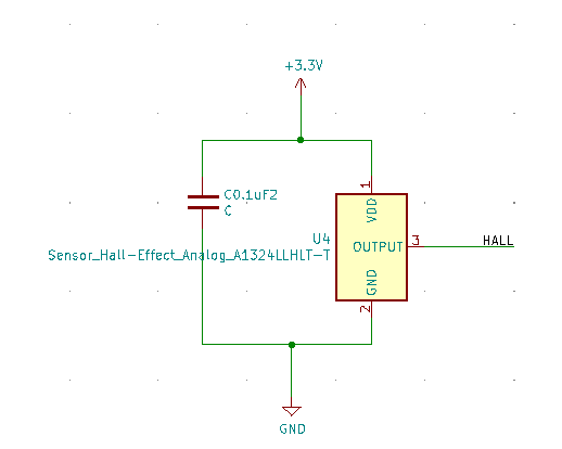
As I wasn't sure that 3-axis accelerometer would work, because it's a difficult sensor I provided a reserve - add also hall effect sensor because it could be easier. For work with HALL EFFECT SENSOR is needed:
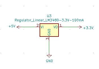
Important thing what need to check how power voltage is enough for sensor - for example for 3-axis accelerometer is necessary 3.3V for that I add a new component which regulate voltage level:
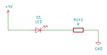
Also I added one feature - it show me that power connection work right, in that case LED light ON:
KICAD SOFTWARE
STEP 1 : SCHEMATIC PART
- How to work with KiCad schematic I explained in Fab Academy Week:07 "Electronics Design"
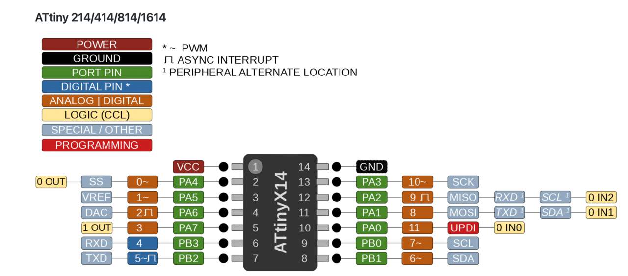
- To understand Attiny1614 pins very useful is a schema by SpenceKonde from GIT.
- To understand what elements I also needed for this chip I read Fab Academy week "Embedded Programming" and this schema for me was very useful:
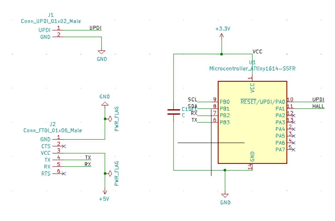
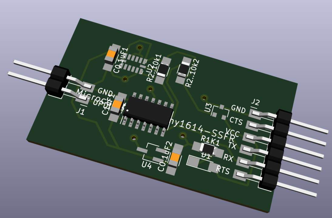
- Result in schematic parts looks like that:
- In pinout picture seen that PB2 is to TX and PB3 is to RX, but actually you need it flipped and PB2 connect to RX and PB3 - TX, it's because from FTDI connection you cannot send data to other TX - you need to use RX because you want that data would be receive.
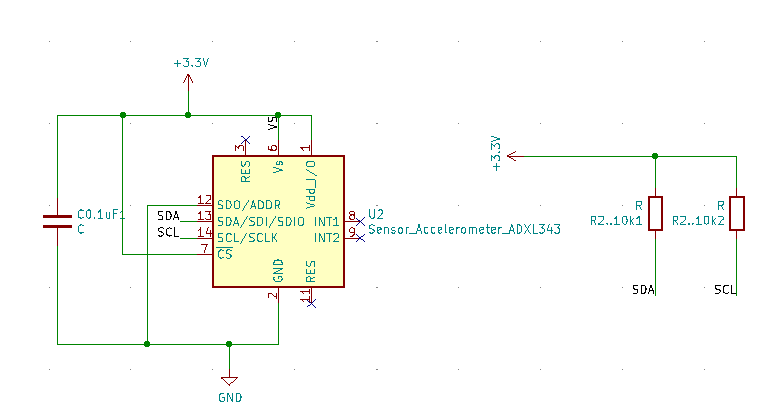
- 3-axis accelerometer in schematic parts looks like that:
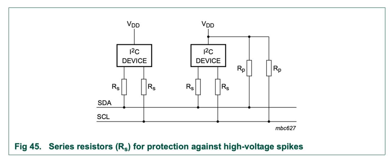
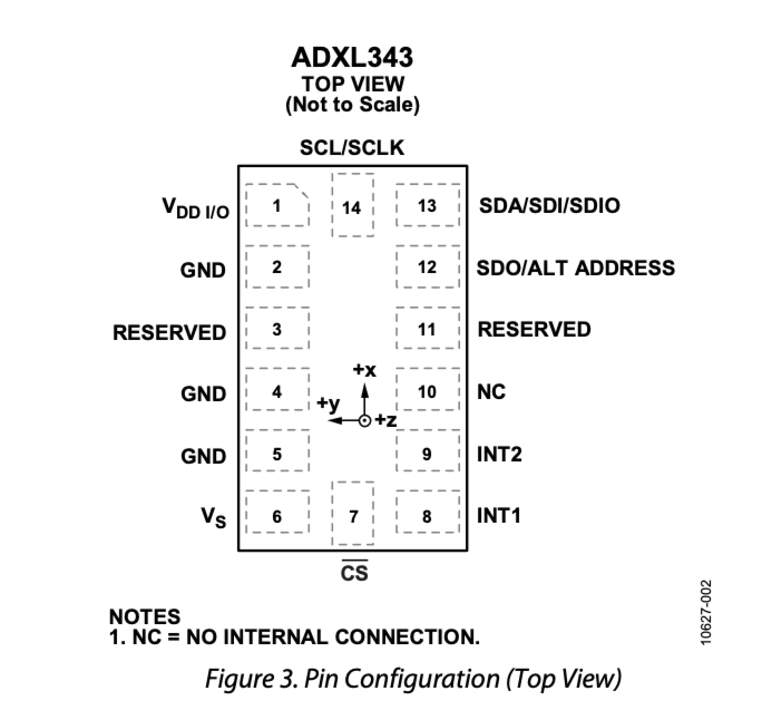
- I invested a lot of time to understand which pins are needed to connect to resistors and for that I needed to understand the functionality of the sensor's chip pads. I read datasheets by "Analog Devices, 2012" and "I2C-bus specification and user manual" and helpful for me was this figure:
- Hall effect sensor in schematic parts looks like that:
- Linear regulator in schematic parts looks like that:
- Power LED in schematic parts looks like that:
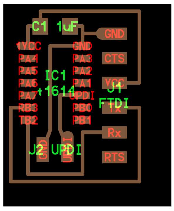
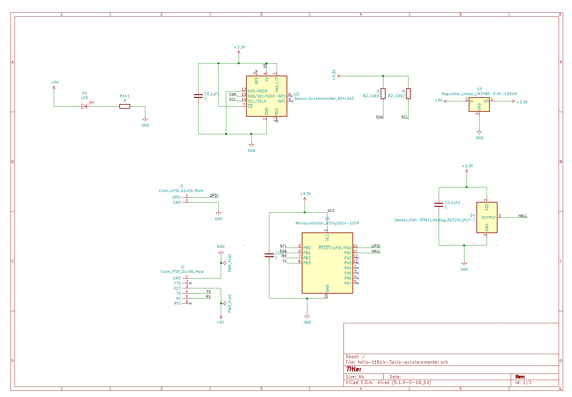
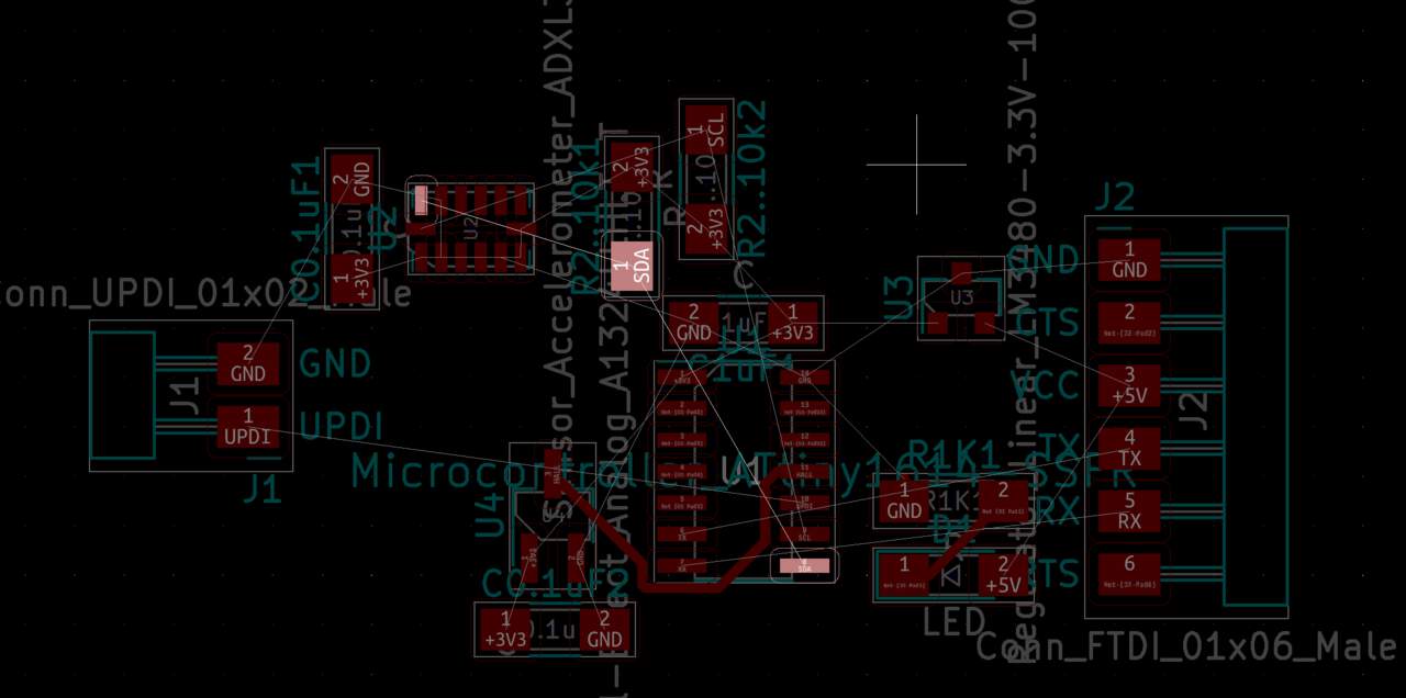
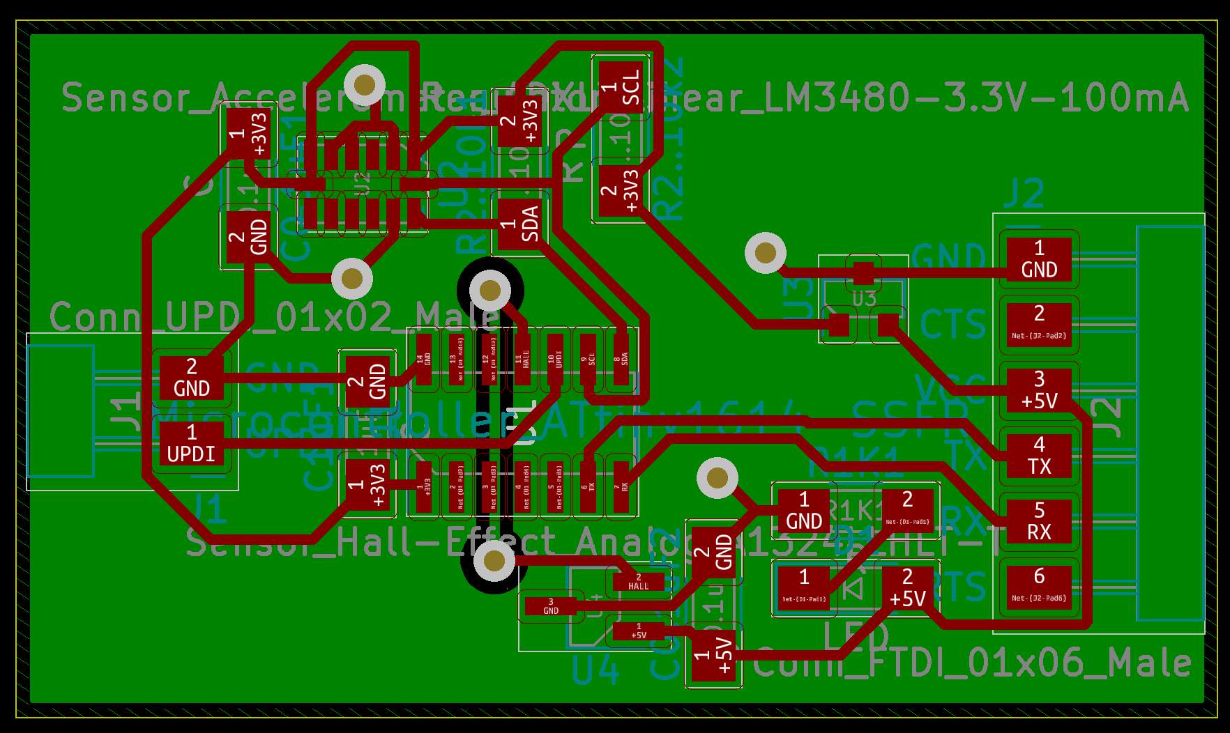
- .. and together it looks like that:
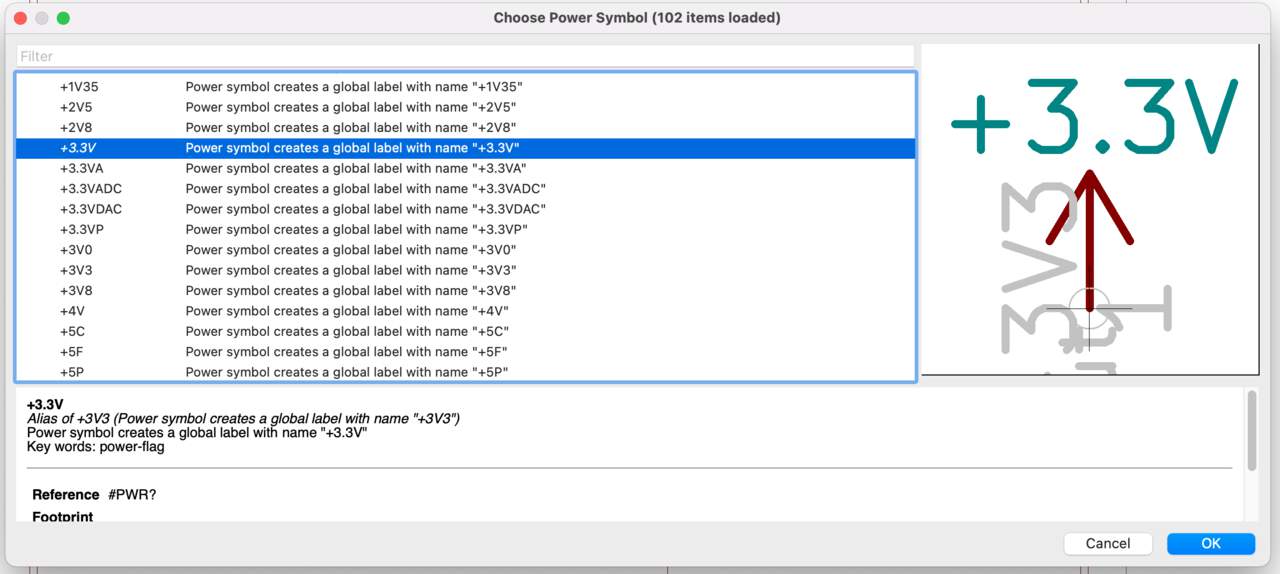
- As you can see in schematic I used Place power port tool and it gives me choose add symbols like Power 3.3/5 for that is necessary download KiCad symbols library from Github (by KiCad) and in Global Libraries added a new Symbol Library power.lib (explanation in Electronics Design week)
STEP 2 : PCB EDITOR
- Also how to work with KiCad PCB editor I explained in Fab Academy Week:07 "Electronics Design"
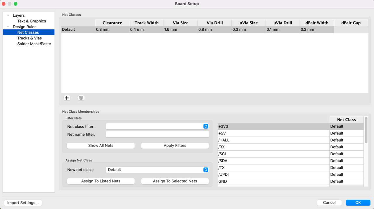
- Nevertheless, I left a note here about Design Rules - Net Classes because later it will become relevant. I defined Clearance = 0.4mm
- ❗ One hint what I forgot added in previous week and when I start to do this week assignment I need again check how I can move connection line. Answer is - Select line and hit D
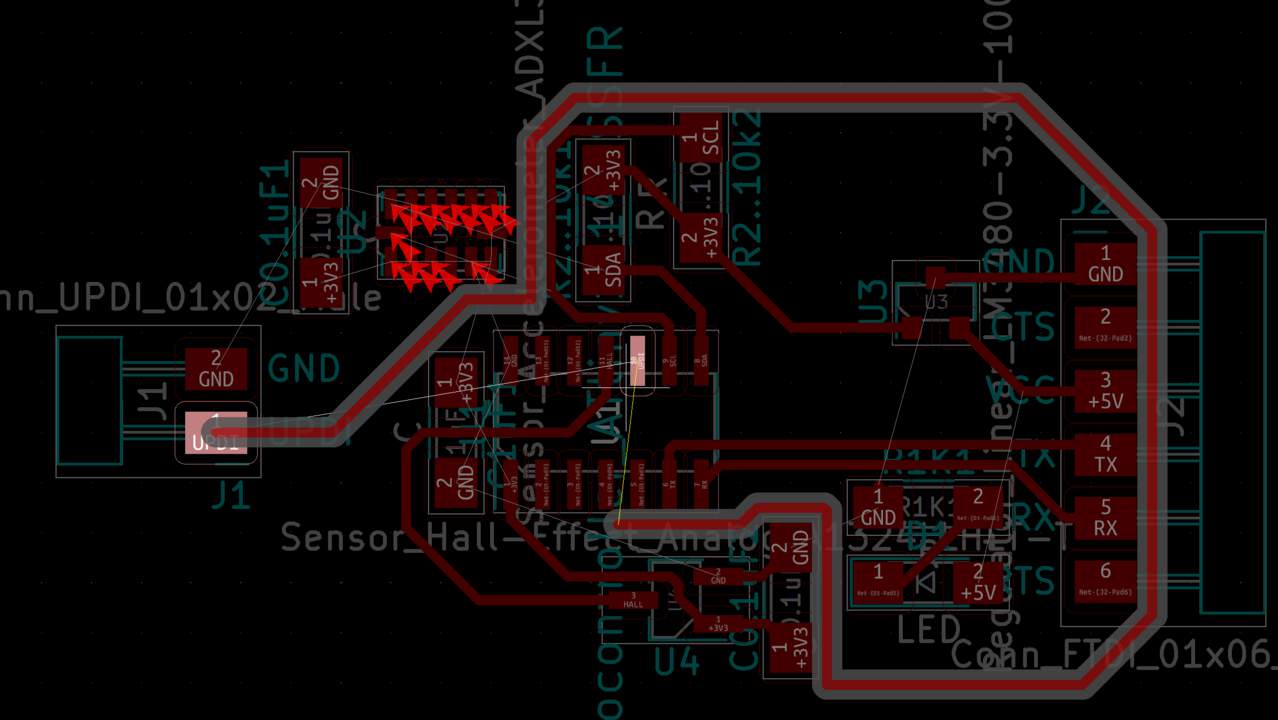
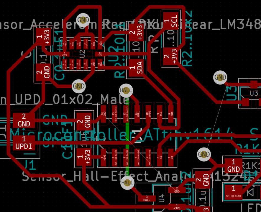
- Of course I spent a lot of time drawing connection lines, because every time some of them were trapped. After my effort the best result I had is that all lines are connected except GND.
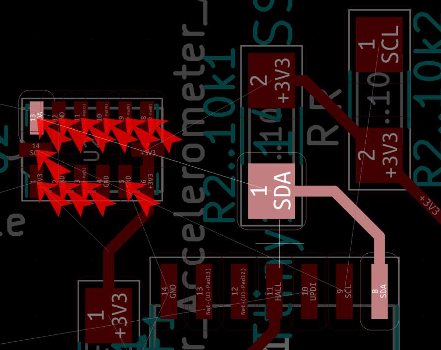
- Interesting thing is in the third picture - I couldn't understand for a long time why I can't connect the chip's SDA with the sensor's SDA and I'm not sure, but I think that software predicts that later isn't a way how to connect the sensor's +3.3V pin. For solution I just flipped chip of the sensor.
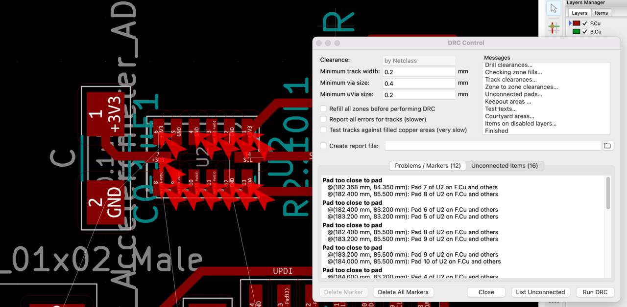
- Times to times I running Perform design rules check and solved Problems and Unconnected Items ❗ but still I have something what I couldn't solved and it related with 3-axis accelerometer. It always said that pads in the sensor are too close but I haven't ideas how to solve that because I didn't do anything inside with the sensor's pads separately. My instructor Kris helps me to understand how I can solve that - just change Clearance to 0.3 mm.. and as always easily explained if you know that, yeah?
- And now go to back with unconnected GND. I conclude that it will be easier to learn how to make double side PCB boards than again try to change others connection lines, rotate, move electronics parts and hope that it will succeed.
STEP 3.1. : DOUBLE SIDE PCB
- All GND I want to connect to the back side.
- Before that check Design Rules - Net Classes especially via values:
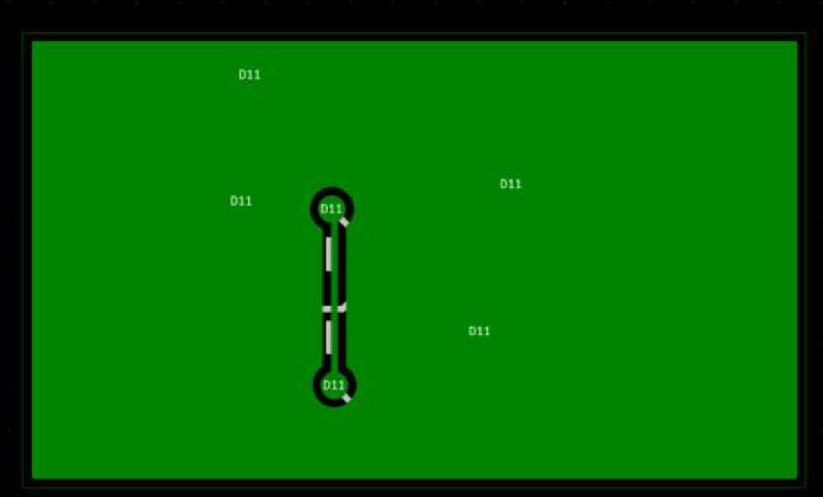
- I choose one of the GND and start to draw line with tool Route tracks and then hit V on a keyboard which stands for via and then click one more time in order to place it and KiCad moves to the other layer (B.Cu(PgDn)) in order to draw the trace and then once you are satisfied with the location hit again V and place via and then you are back to the main layer (F.Cu(PgUp)) so now you have a two layer connection. At this moment I also understand that it would be a good change also another connection and in the result not only GND have in the back side but HALL connection too.
- To connect all GND I used another feature which was called Add Filled zones. Go to (B.Cu(PgDn)) layer by using the layers selector. Start to draw a filled zone and shall be marked so that the landfill covers at least part of where GND is located. When opened Copper Zone Properties choose the right layer and specify which is going to be NET which in this case is GND. Then hit letter B and it's then connecting everything together.
STEP 3.2. : NOT NODES BUT ANOTHER SOFTWARE
- As I plan to do the milling part in another way (not as previous week in nodes) for outline I choose Edge.Cutslayer and Add graphic lines to draw outside lines.
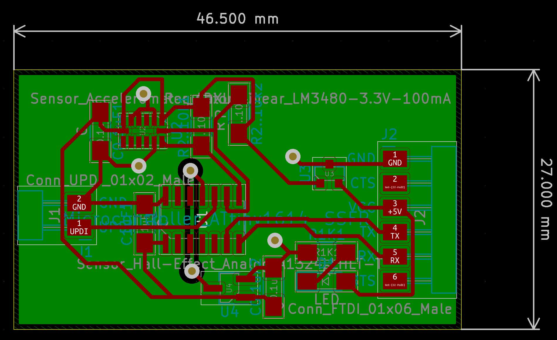
- Result (with included previous filled zones step) looks like that:
STEP 4 : MAKE A GERBER
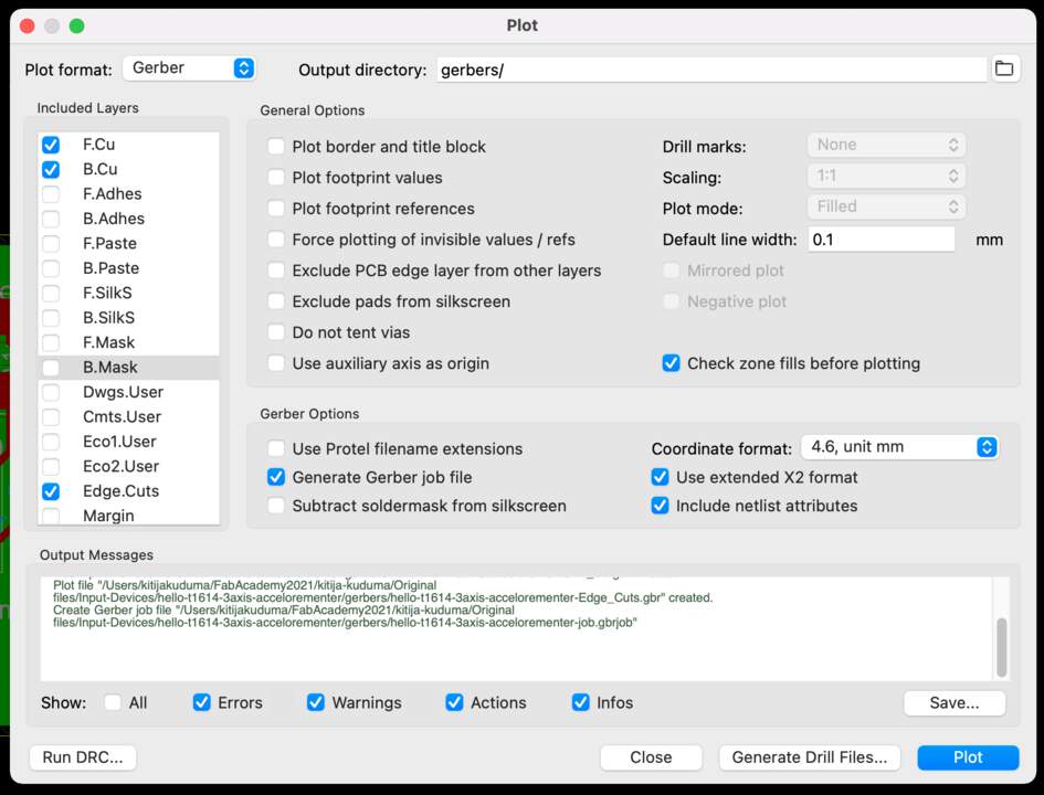
- Plot a GERBER format is necessary for next steps when I plan to work with another software for milling my PCB.
- Click on the PLOT button, select just F.Cu, B.Cu and Edge.Cuts layers, define location where it saves your GERBER and unclick unnecessary options (look at picture).
- Then click on the Plot button. It generated gerber files.
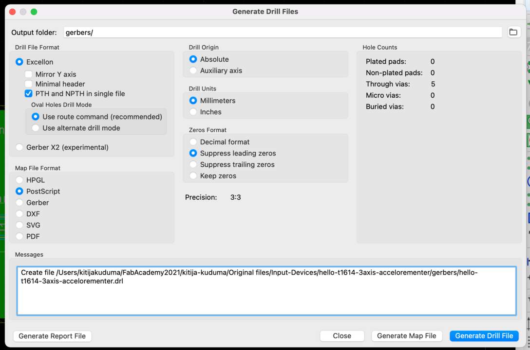
- Another thing that is needed is to generate drill files, look at picture what option is needed and then click on the Generate Drill File button.
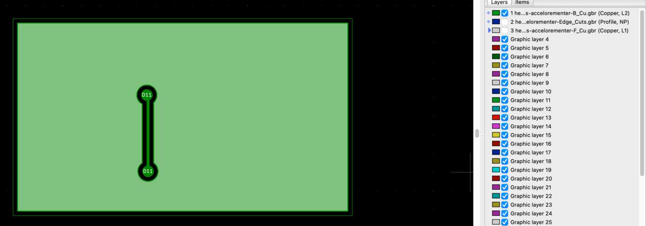
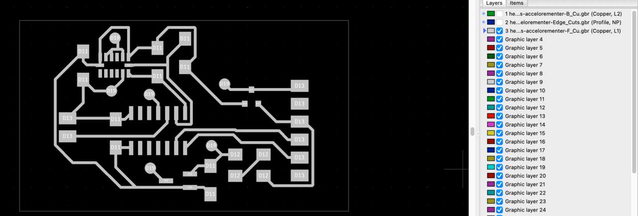
- To check that all files generated right KiCad has a plugin Gerber Viewer. Open it and import generated files and just check how looks all layers.
RESULT OF ELECTRONICS DESIGN PART
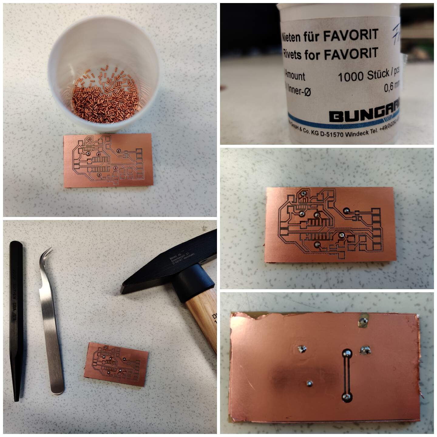
STEP 5 : PCB MILLING WITH COPPER CAM SOFTWARE
- Open the CopperCAM software. Open - New circuit and import gerber file (start with the front copper (F-Cu) layer).
- In Dialog Box Board dimensions Reframe around existing circuitry with a margin of 2 mm is good, Z thickness is the thickness of the circuit board in FR1 case - 1.6 mm.
- If received message "Tracks" then you need to configure whether the path that is selected that is highlighted red lines is actually the outline or the contour of the circuit board. Click Yes button.
- CopperCam placed all the traces on the first layer (Layer#1) and the outline on the second layer (Layer#2), Edge cuts ar on the layer number 6 (Layer#6).
- Import the drill files for that click on the File - Open - Drills.
- Select the layer #5 where the drill points are actually placed and then if holes are not imported in the right direction click on the File - Rotate 90 how times are necessary.
- Go to Layer#1 and define a reference pad - choose one of the traces drill points which you want to specify as a reference. Right click - Set as reference pad. Now selected coloring in pink color. The selected point you want to map to the appropriate hole. For do that - go to the drill layer, select hole - right click - Adjust to reference pad #1. Repeat it with second reference on the other corner, set as reference pad #2 and then all holes go in the right place.
- Next thing is to be sure that the hole sizes are set according to what you want. Be in the Drill layer - Right click on ones of the holes - Change diameter - Drill - 1 mm. Be sure that change both of references - #1 & #2. If you want to insert rivets then change diameter to 1.5 mm.
- Make sure that the margin around the circuit board is the same for that go to File - Dimensions - hit OK and it recalculates.
- Next thing is specify the origin for that go to File - Origin and set X:0, Y:0.
- Now about how to create the toolpaths - Go to Preferences - Selected tools:
- Engraving tool: 0.1-0.15 mm, diameter 0,2
- Hatching tool: 0.1-0.15 mm, diameter 0,2 (the same Engraving tool)
- Cutting tool: 1 mm
- Centering tools: 1 mm, diameter 2
- For Drilling tools if you have the same diameter size drill holes on your circuit board you could use a single tool for all drills
- Drilling depth: 1.8 ( a little bit more than FR1 thickness), Borung speed: 5 mm/s.
- Go to the layer #1, click on the Calculate contours, Number of successive contours: 4(but if you still have unremoved parts you can set a bigger offset), Extra contours the same and check in settings below.
- For exporting toolpaths click on the Machine - Mill button:
- Engraving layer #1 - in double side PCB boards click on the Mirror X, Speed - 10 mm/s, set XY-zero point as White cross. Z-zero point - Circuit surface. Hit OK and make a new folder, for example, Milling and save it with a logic name and optionally with tool diameter, for example "engraving_0p4mm".
- Then go to the menu again and instead of engraving choose Drilling with 1mm tool and save it, for example, "drilling_1mm".
- Then again - choose Cutting out with 1 mm tool.
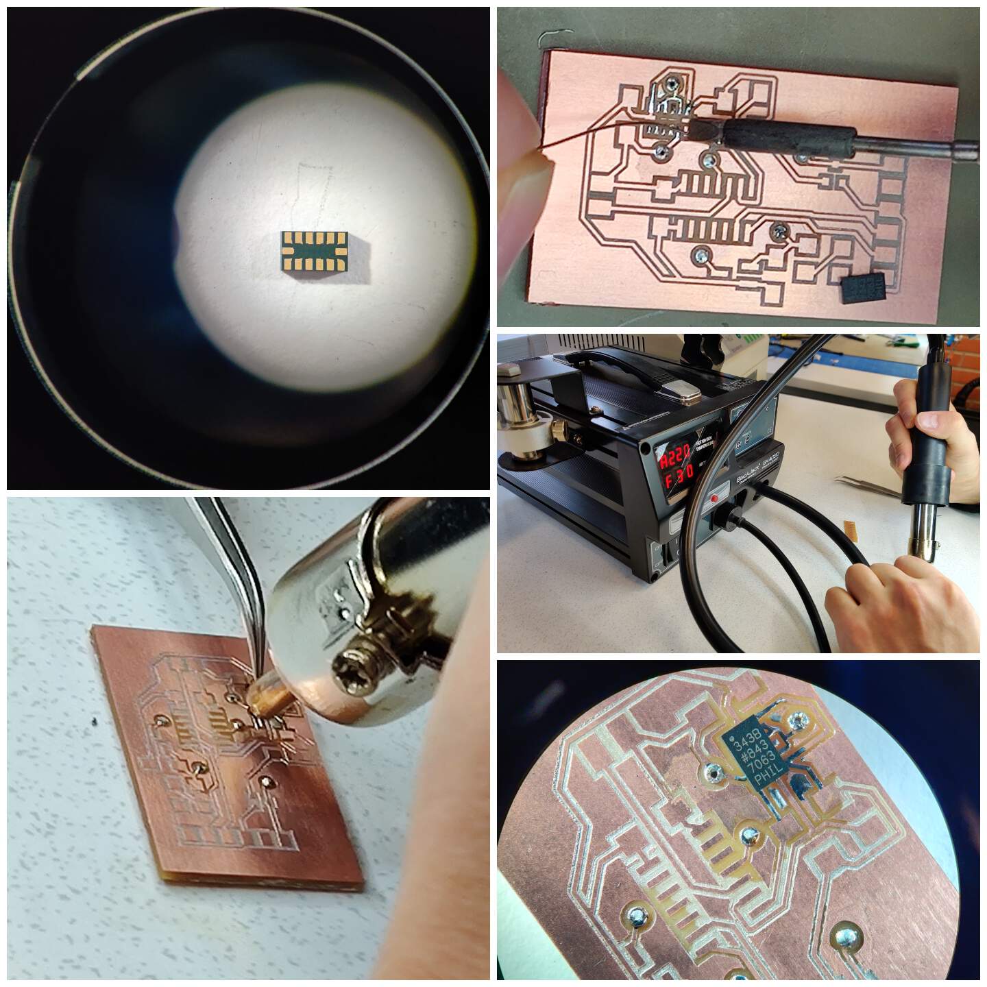
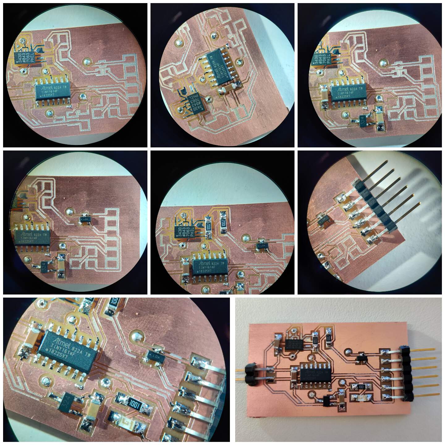
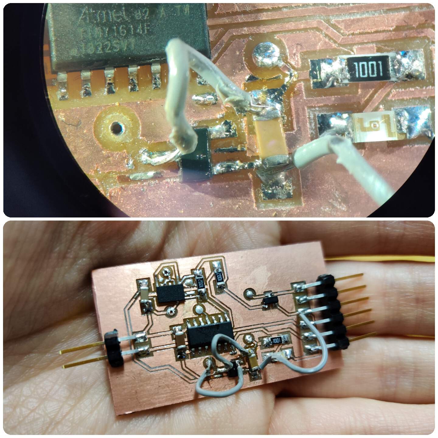
STEP 6 : SOLDERING PART
- In this week soldering part is more challenging because two new things:
❗ The first thing is that 3-axis accelerometer cannot endure the solder heating temperature. For that is needed one tip & trick - heat gun equipment.
❗ The second thing is that this was the first time when I use vias - Otherwise the whole process is the same as in previous weeks.
STEP 7 : PROGRAMMING PART
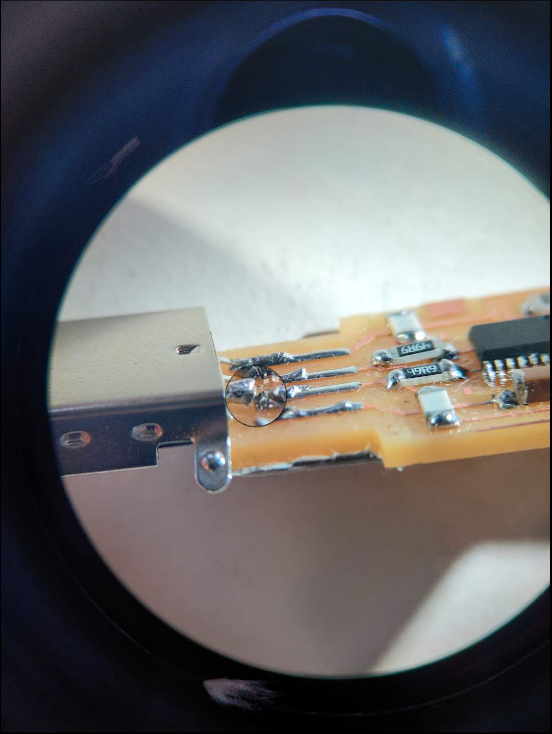
- As every programming week my UPDI had unsoldered again. At first it seemed that the new PCB board wasn't working, but the microscope helped to clarify the problems with UPDI.
- Then I tried to create code to check that my new board could communicate.
This video not included in GIT, because size of it is more than 8 MB also after video optimization.
- Then I tried programming the Hall effect sensor so that it can read values and send them in the Arduino Serial Monitor. First goal was that source code works, but I concluded that values are reading but not correctly.
                //Original code comes from Adrianino (Fab Academy 2020), I just adjusted it my own pin and initialized serial communications
            int sensorPin = 8;   // analog input pin
            int sensorValue = 0;
            void setup() {
                Serial.begin(115200);}
            void loop() {
                sensorValue = analogRead(sensorPin); // read the value from the sensor
                sensorValue = map(sensorValue, 0, 1024, 1024, 0);
                Serial.println(sensorValue);
                delay(500);}
STEP 8 : THE MOST VALUEABLE PART - FIND & SOLVE FAILURES
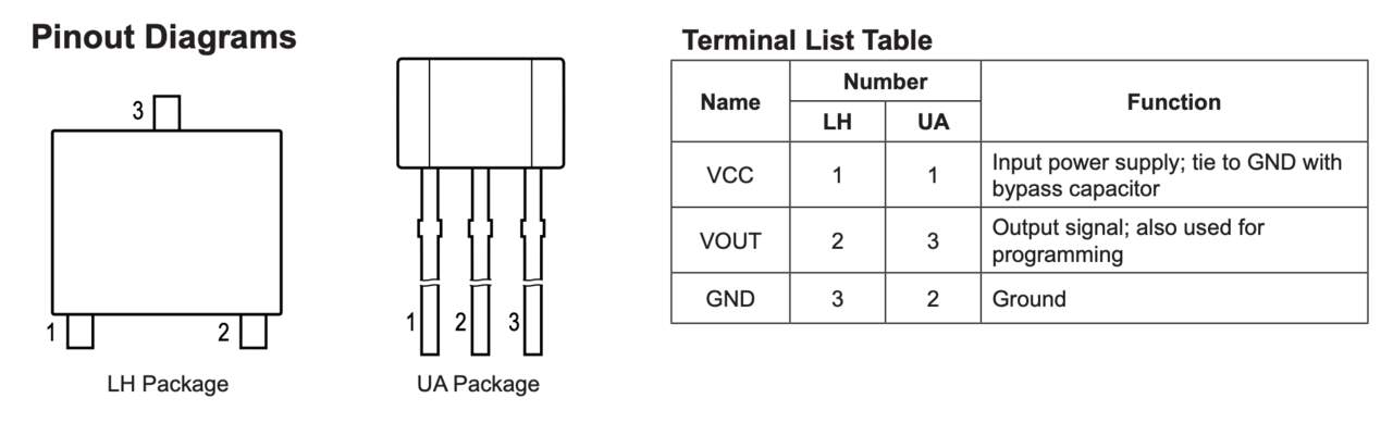
- ❗ Hall effect sensor's need not 3.3V but 5V.
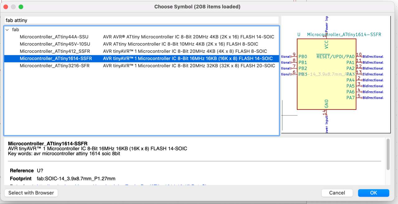
- ❗ As for using fab electronics components I some weeks ago downloaded Fab KiCad library from GIT (by Kris), but my mistake I just downloaded it, but
it would have been much wiser to clone it. Why? Because there may be updates. Lesson - always clone GIT libraries and before start to use them
update it in Terminal with commands
git remote updateandgit pull. And as a Murphy's Law - there were updates directly to the Hall effect sensor - GND and OUTPUT must be swapped. Now I also checked it on the datasheet (by Allegro microsystems). - ❗ If something has to be reversed, then it is quite easy to solve with jumper wires. The strange thing was that after adding jumper wires, the sensor started to read maximum possible values but still incorrect values were read.
- ❗ For that I again tried to something change - added more solder for stronger connection but then the sensor started to read just one value - 1. With my instructor Kris we concluded that a short circuit occurred.
- ❗ In original files all these failures are solved.
"HERO SHOT" VIDEO - RESULT
VISUALIZATION OF THE DATA : CODE
- I used the programming language Processing to visualize the data. This programming language is known as a way to visualize data, especially in demand among designers.
- Comments are left behind // to better understand what's going on in the code.
//Original code comes from Adrianino (Fab Academy 2020), I just adjusted it for me
import processing.serial.*;
float sensorValue; //variable for the serial data
Serial myPort;

void setup() {
  size(1024, 200);// is the window (1024=sensor max. value)
  myPort = new Serial(this, "/dev/tty.usbserial-FTBBWTWN", 115200); // serial port
  background(255);  //set background white
}
void draw() {  //draw function loops
  noStroke(); // outline
  fill(255,0,0,20); // color inside
  rect(0, 0, sensorValue, height); //position and size

  fill(255,70);
  rect(sensorValue, 0, width-sensorValue, height);

  println(sensorValue);
  fill(0,0,0);// these are the colors inside
  text(sensorValue + " " , sensorValue, height/2);
  textSize(32);
}
void serialEvent(Serial myPort) { // sketch read the serial data
  String inString = myPort.readStringUntil('\n');
  if (inString != null) {
    inString = trim(inString);
    float[] values = float(split(inString, ","));
    if (values.length >=1) {
      sensorValue = values[0]; //first value in the list
    }
  }
}
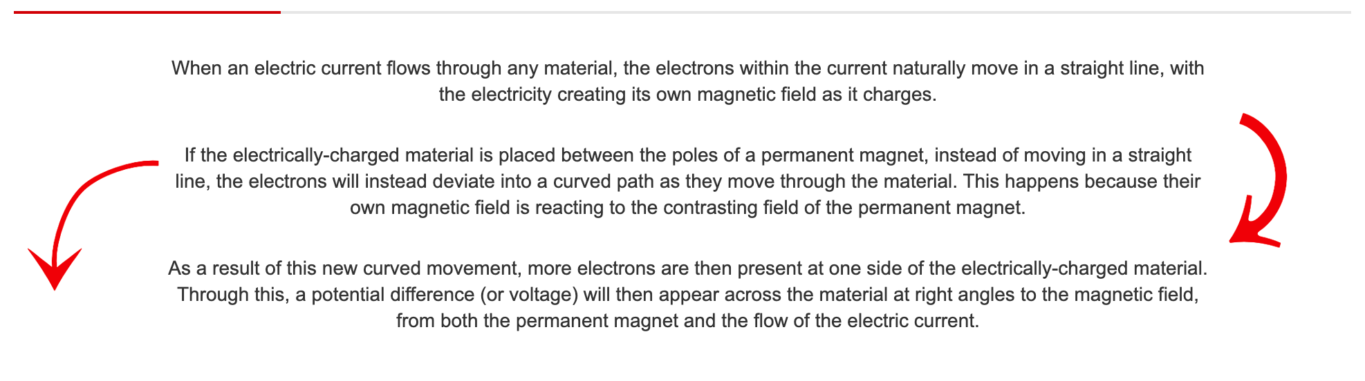
HOW HALL EFFECT SENSOR WORKS?
- Video can be seen in an interactive way - as the PCB moves away from the magnet, the fixed distance increases, when zoomed in, the fixed distance decreases. But how does a sensor know that it is moving away from or approaching a magnet? What's going on inside? "Hall" because it is named after the physicist Edwin Hall. He discovered that electricity and magnetism can work together. Hall effect sensors convert magnetically encoded information into electrical signals. Hall effect sensors work by measuring the changing voltage when the device is placed in a magnetic field. It detects that it is now in a magnetic field and is able to sense the position of objects. A more detailed explanation of the magnetic field by RS Components AB is attached below.
SOME NOTES | CONCLUSIONS:
- I noticed that when my PCB is connected to the power supply, the hall effect sensor does not immediately read the values and as I read in the datasheet about Power - On Time- the device output requires a finite time to react to an input magnetic field. And it happens after the power supply has reached its minimum voltage.
- I tested that it doesn't matter on which side I approximated to magnet still values are close on both sides.
- As I read in the same datasheet the device sensitivity and precise values are dependent on environment temperature.
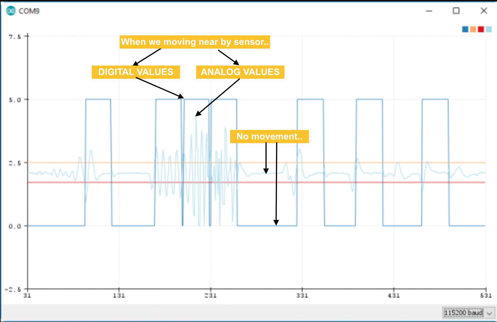
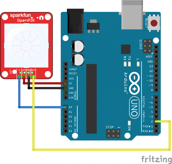
STEP 9 : GROUP ASSIGNMENT PART : PIR SENSOR
- With student Wu Ruo-Xuan we tried to understand what an OpenPIR sensor is in the lab - how to program it and what to measure with it. PIR is a passive infrared sensor which detects motion. To work with the sensors, it is important to find out how much power it needs. In the case of SparkFun OpenPIR - range is 3V to 5.75V as we known it from the datasheet. It means Arduino for that is enough. To connect the sensor to the Arduino microcontroller, we used the instruction from learn.sparkfun. One note - this sensor only responds to movement and that means if you are putting your hand in front of the sensor and don't move it - the sensor will measure it as immobility. Also the sensor has one feature to understand that movement is recognized - LED turn on in movement. How to build code we learn from here. From the first measurements, we didn't quite understand what was going on in the code and graphics, but the instruction explain it well. Now we also know what the orange and red lines in the figure mean - "it represents the upper and lower thresholds, which the analog value must exceed the trigger motion" (by learn.sparkfun).