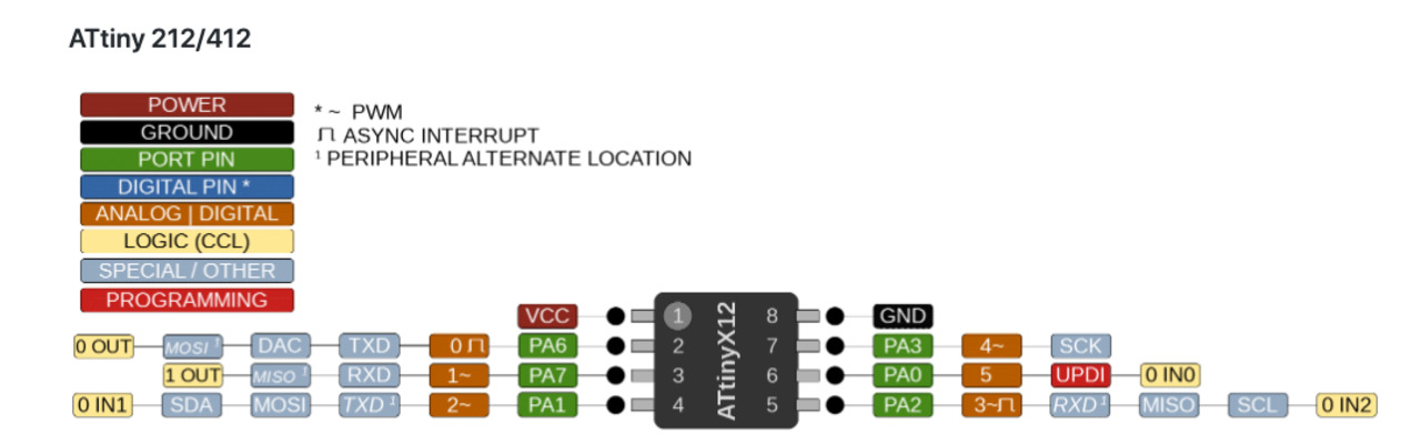
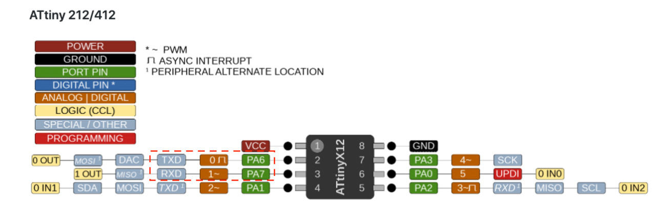
ATtiny412
- VCC and GND is the part where you provide voltage to the chip so you provide power.
- Green pins PA0, PA1, PA3, PA6, PA7 are programmable, but some of them have special functions - No.6 or PA0 is the UPDI programming pin. Also PA6 and PA7 are also programmable, but these are TX and RX which stands for basic serial communication. When you are going to connect an FTDI cable to it the operating system is going to establish a serial connection and through this serial connection you will be able to talk with the chip by using resending and receiving bits and bytes.
KICAD SOFTWARE
STEP 1 : SETTINGS
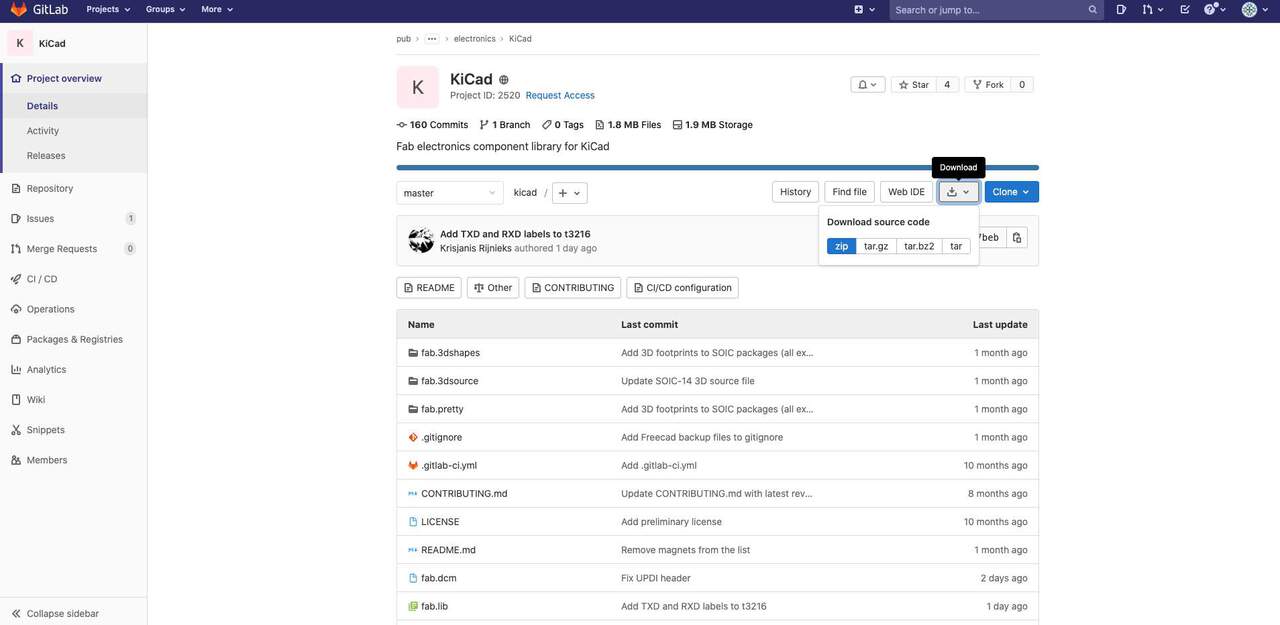
- In order to use the KiCad library (by Kris) you need to download it from GitLab.
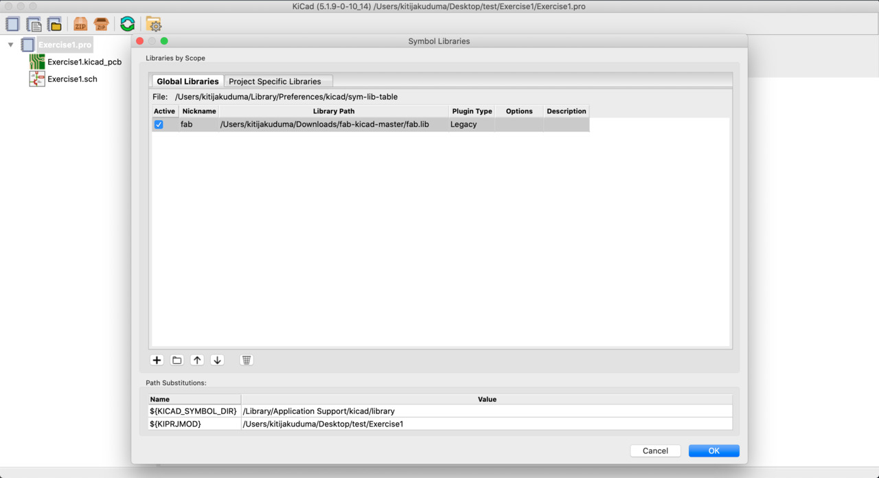
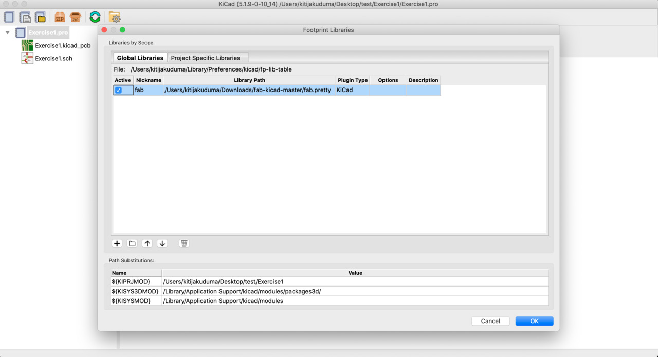
- Then open KiCad software and in order to use this library you should go to Preferences and the first the main part that you need to do is to click on the Manage Symbol Libraries and import fab.lib file from the downloaded KiCad library. After that click on the Manage Footprint Libraries and import fab.pretty file.
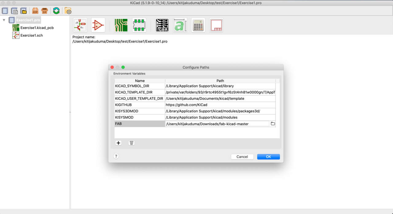
- And the last thing is to configure paths for that click on the Configure Paths and define a variable that is called FAB (capital letters).
- Then you can start out by creating a new Project and after that you can see that KiCad creates two files for you - one is the schematics file and the other is the PCB file.
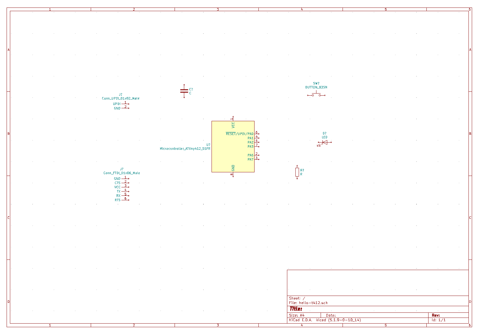
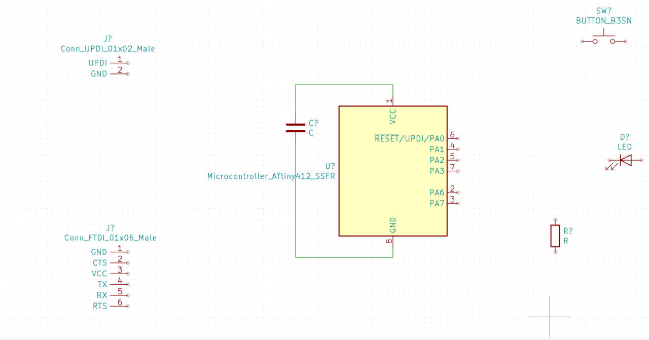
STEP 2 : LET'S START WITH A SCHEMATICS FILE - ADD COMPONENTS
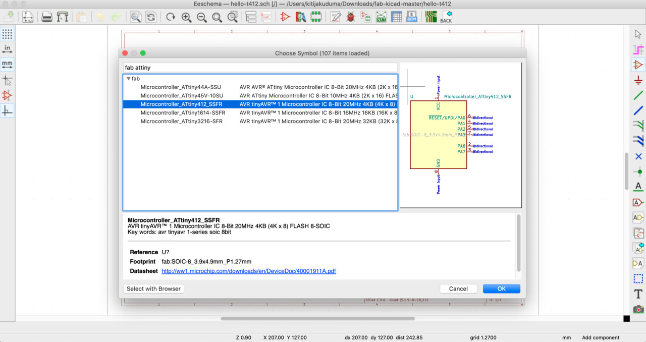
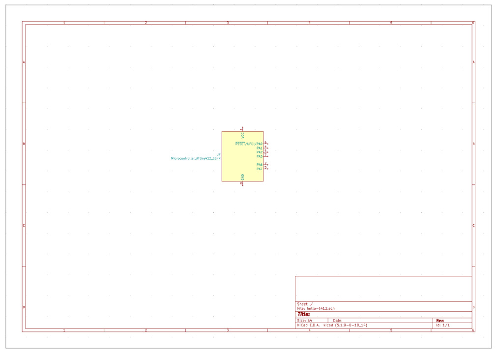
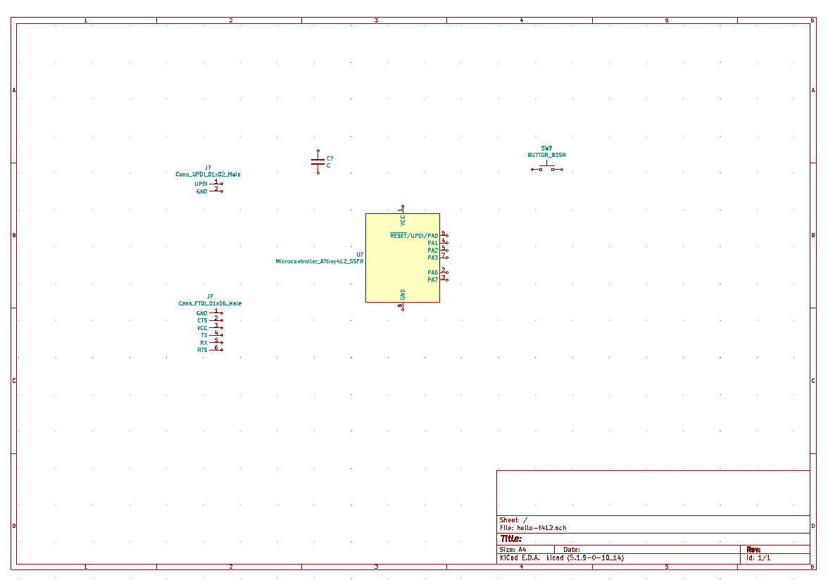
- In the right side select the Place Symbol button and find the component with keywords "fab attiny", select 412.
❗ There are a whole packet convention in that explains the best practices how to design these sort of symbols and usually the rule is that you put positive voltages on the top, negative voltages on grounds on the bottom and all the connections on the sides - usually inputs on the left side and outputs on the right side.
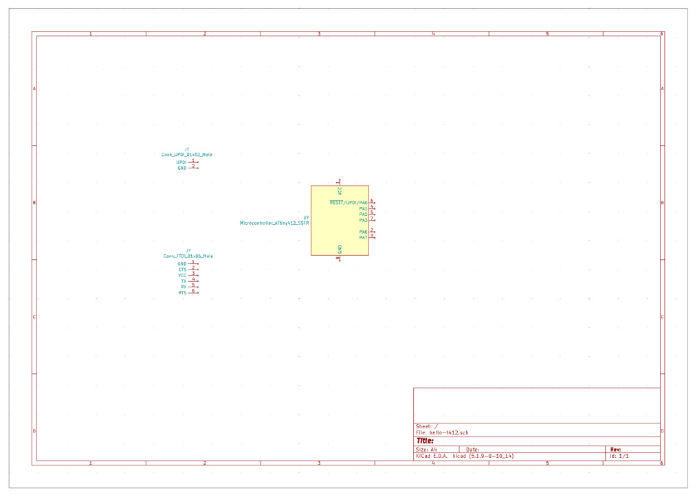
- Then add UPDI component in the same way.
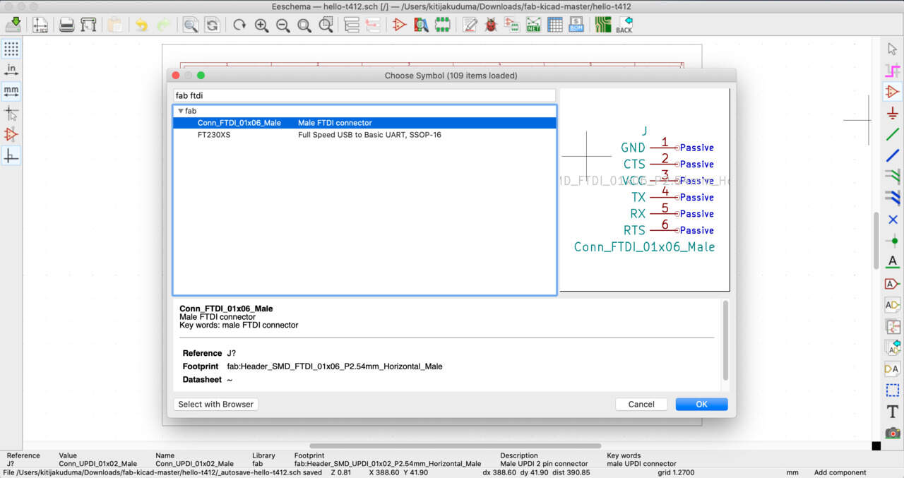
- Then add FTDI component in the same way.
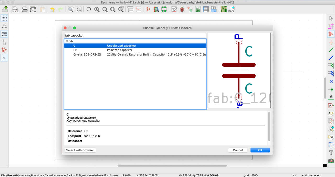
- Then add Capacitor in the same way.
❗ There are two types of capacitors - the unpolarized capacitor and polarized capacitor. Unpolarized you usually use to filter current for microcontrollers and different kinds of other integrated circuits, but when you are working with motor controllers, amplifiers or audio filters that you might use more polarized capacitors.
.. in this case you need to choose an unpolarized capacitor. - Then add Button in the same way. There are two types of buttons, choose B3SN.
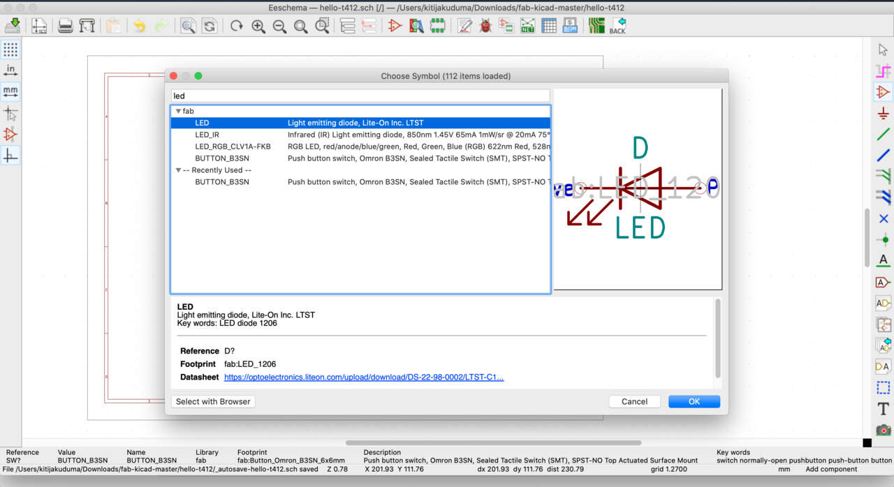
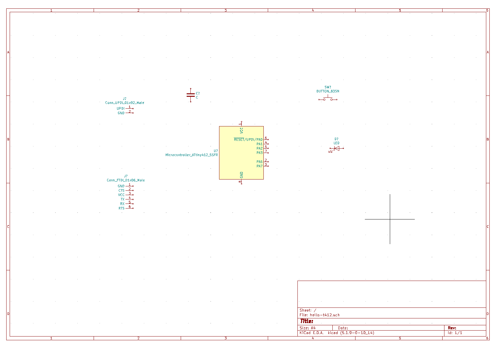
- Then add LED, choose simplest.
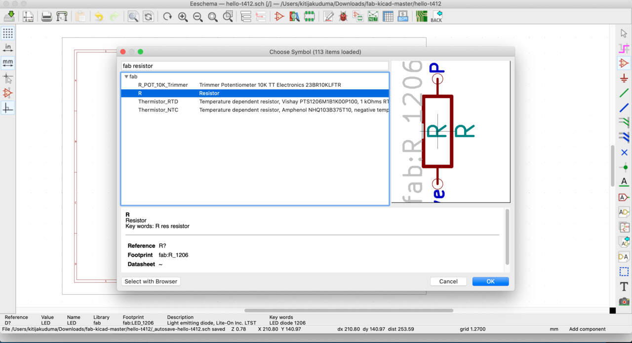
- Then add Resistor component in the same way.

STEP 3 : HOW TO CONNECT COMPONENTS TOGETHER
- Choose the Select item tool.
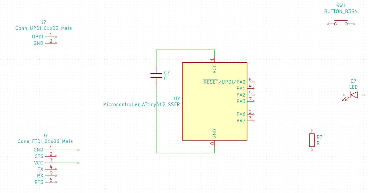
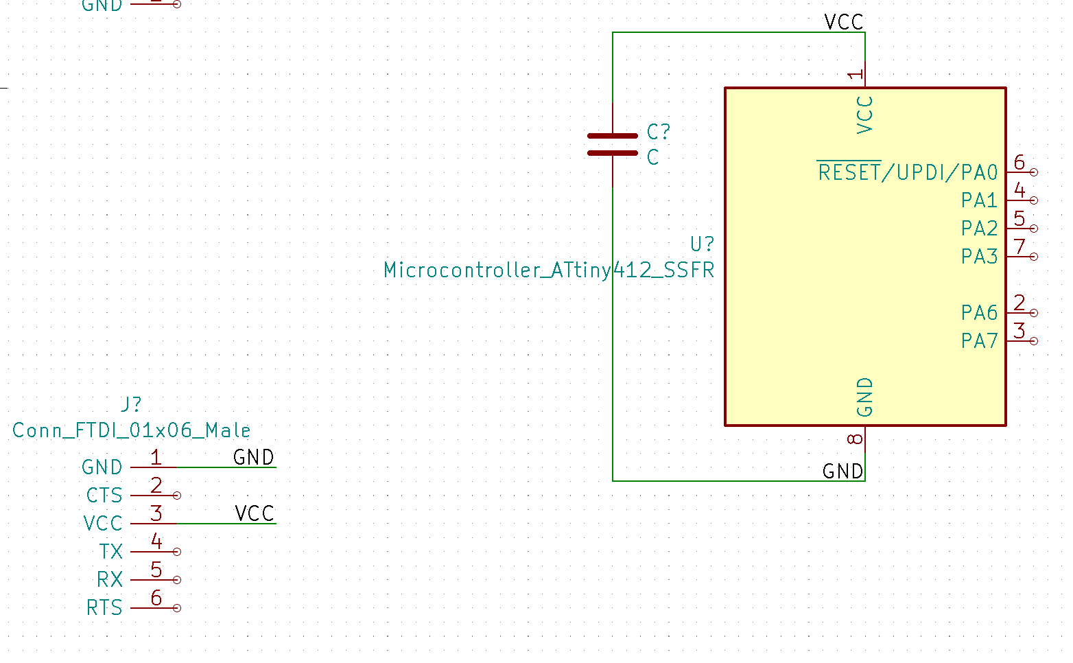
- Capacitor you need to connect to VCC and GND directly.
❗ In schematic it doesn't really matter where it is located, but on the real board it's going to be important to put it as close as possible
to terminals to filter the current through it for the VCC and GND. To protect the chip you need to use this capacitor it's going to make
sure that the current flows smoothly into it.
Move the capacitor closer to ATtiny. - Choose the Select wire tool and start to draw.
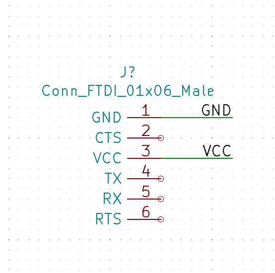
- You need to specify where the voltage comes from and in this case it's gonna be the inputs are gonna be the FTDI connection.
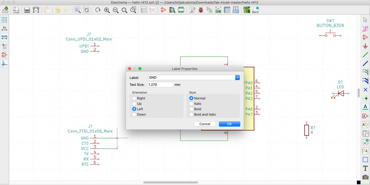
- Now place the label - press letter L. Select the Orientation - Left and Label name "GND".
- Repeat it with VCC.
- Then in order to connect to the capacitor wire add just labels.
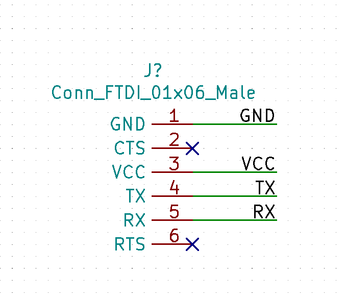
- From the FTDI connector the two pins that are going to use except the ground and VCC are going to be the TX and RX pins. CTS and RTS in this case not significantly - just put the Place no connection flag symbol of them. For CTS and RTS use again drawing wires and in this case also going to use labels.
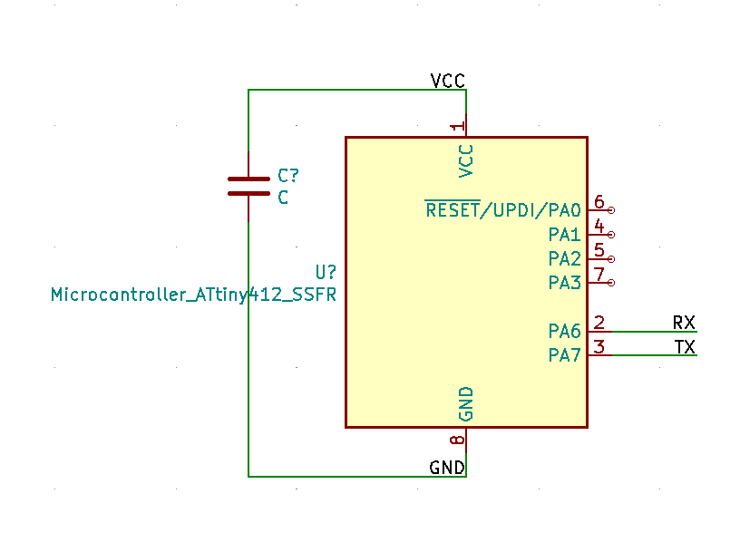
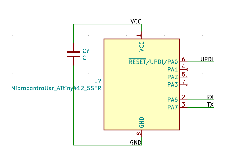
- Now it is important to understand which of ATtiny412 pins are the hardware TX and RX pins - for that you need again check the first picture from this page (ATtiny). It can be concluded that PA6 is to TX and PA7 is to RX, but actually you need it flipped and PA6 connect to RX and PA7 - TX, it's because from FTDI connection you cannot send data to other TX - you need to use RX because you want that data would be receive. After that again drawing wires and using labels.
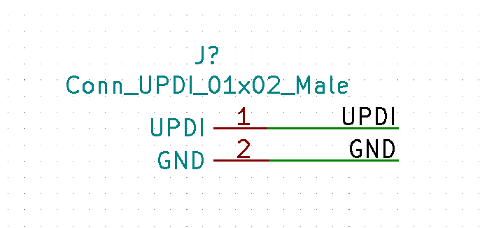
- From UPDI also draw some wires and add the ground label and UPDI label as well. In order to make a connection you need to draw a wire to the UPDI connection of the chip add a UPDI label over.
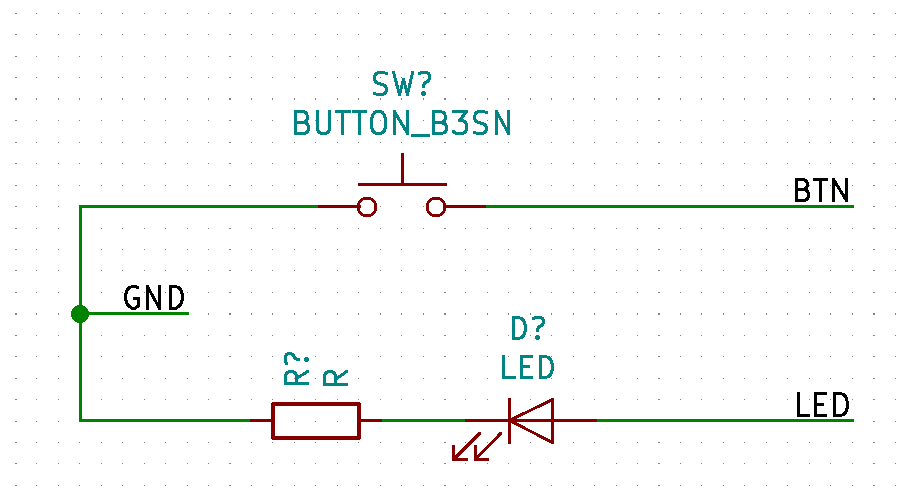
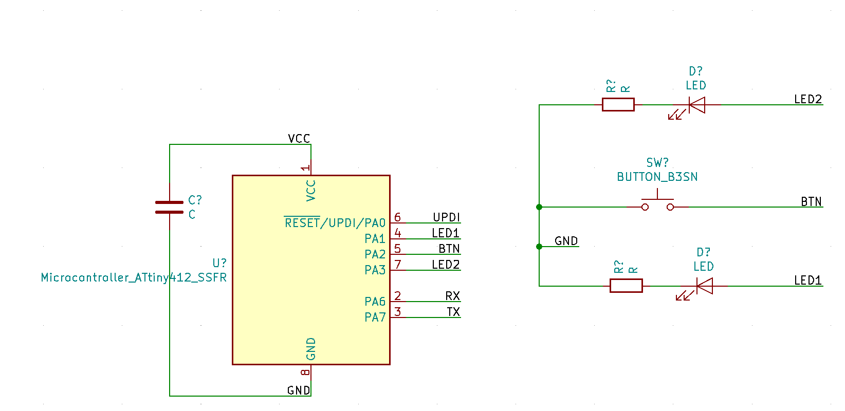
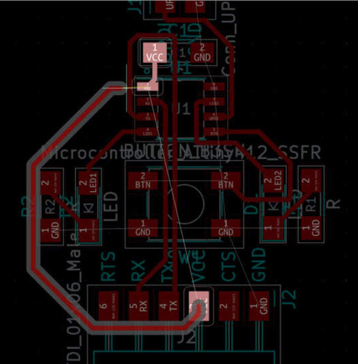
- And the last thing is to connect the button and the LED. Use wires in order to add extensions to those and then some labels. For the button add a BTN and for the LED - LED label. Then connect the resistor and LED. And connect Button and resistor, because you need both of these to connect to ground. For that just create a junction and add a ground (GND) label.
- For BTN and LED in right side you need to connect them to the ATtiny microcontroller's pins. Let's connect BTN to PA2 and LED - PA1.
- Then I add a second LED and don't forget - for each LED you need a resistor.
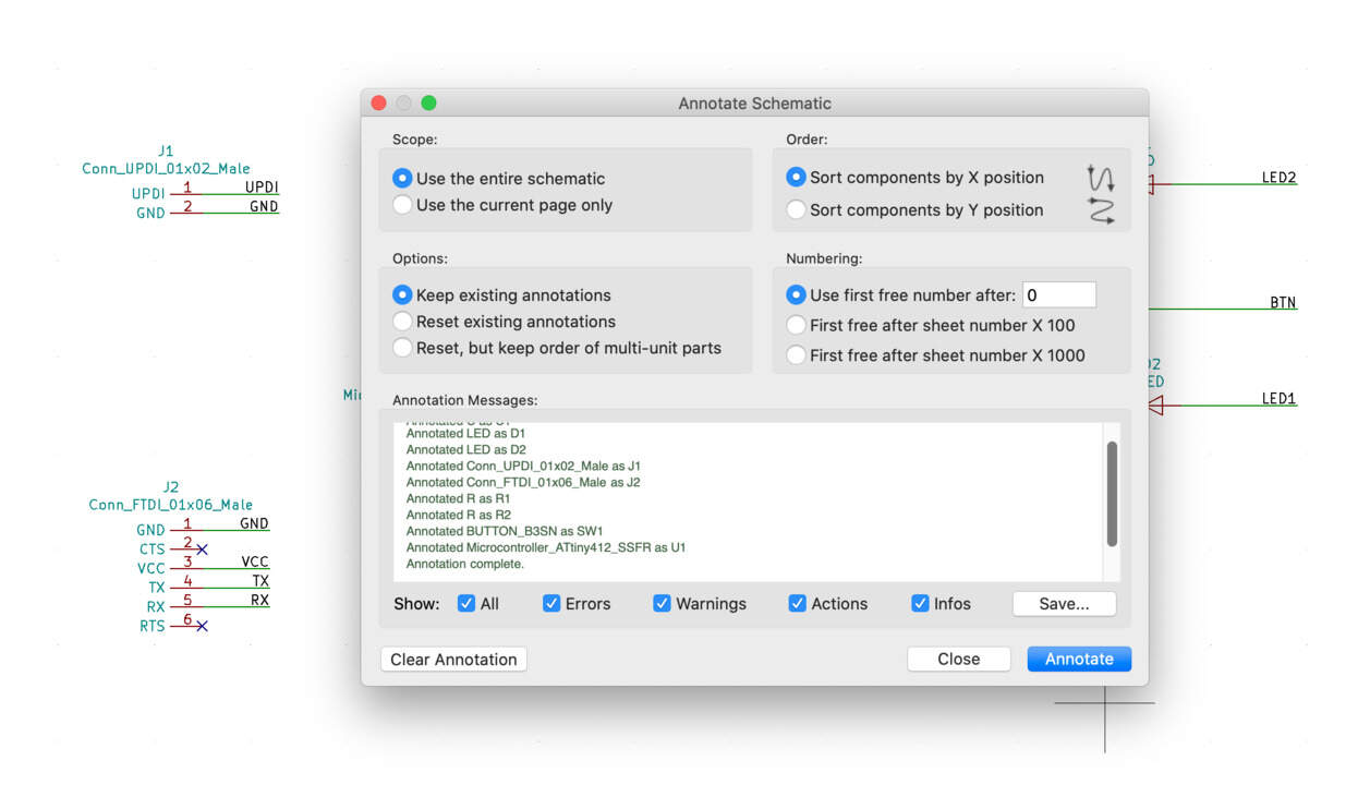
- Then start running the annotate schematic symbols button and click on the Annotate button.
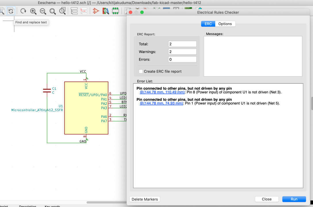
- Then you can press the Perform electrical rules check button in order to check the electrical rules. There are two errors and it complains about some things.
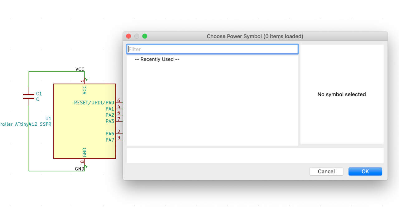
- In KiCad it's important to specify where the power comes in so even though you know that the power comes from FTDI connection anyway you need to explicitly specify where the power comes in by using power flags. Select the Place power port tool from the right side and click somewhere. It's going to open a dialog box and you need to look for the power flag (PWR).
WHAT AN UNEXPECTED TURN : I HAVE A PROBLEM!
- When I opened the dialog box .. it was empty!
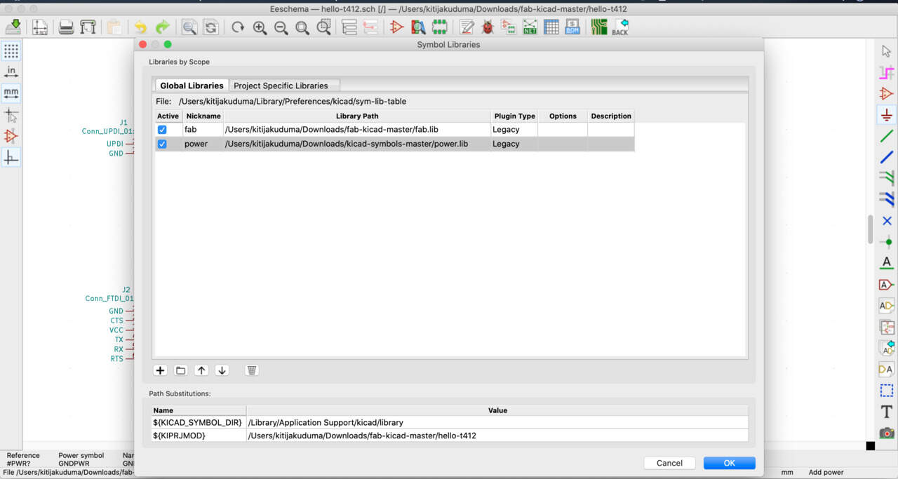
- Then I found the KiCad symbols library from Github (by KiCad). I downloaded it like a ZIP. Then in KiCad software added a new Symbol Library power.lib.
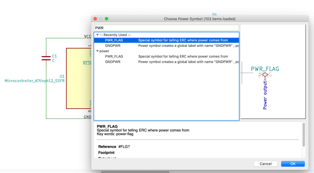
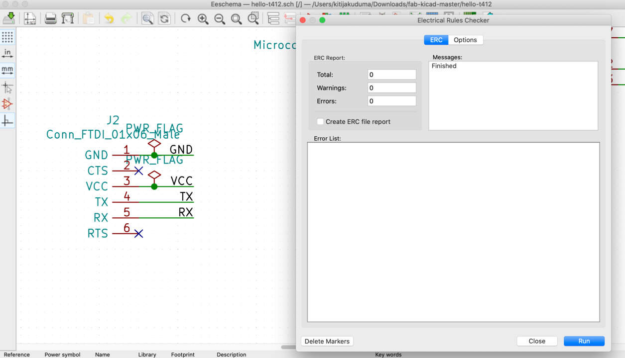
- Now go back to the dialog box.. find the PWR symbol and click somewhere. Then put the symbol in FTDI GND wire and repeat it with FTDI VCC.Then check again what said electrical rules check (bug tool). No bugs!
PROBLEM SOLVED!
SCHEMATIC IS READY!
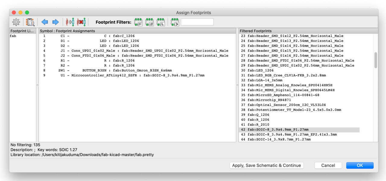
- Usually if you're using the default KiCad symbols you will need to assign footprints to the symbols that you have. For that click on the Assign PCB footprints to schematic symbols. This is the footprint assignment. Just check that all components are assigned.
- Next step is to click on the Generate netlist button and should put it in the same folder where the same project folder which is also opened by default when you initiate it. Once you have your netlist you can move on to the PCB new software which is part of this program by hitting Run Pcbnew to layout printed circuit board button.
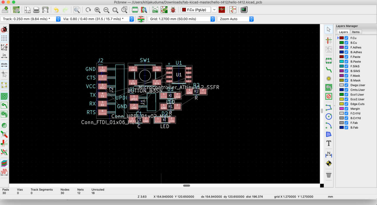
STEP 4 : PCB EDITOR
- In order to open the net list and the parts of the footprints that you're going to be using you have to click on the Load netlist button. Then select the netlist and then hit Open and Update PCB and then you can close the dialog box.
.. AND HERE WE ARE! I HAVE A SECOND PROBLEM
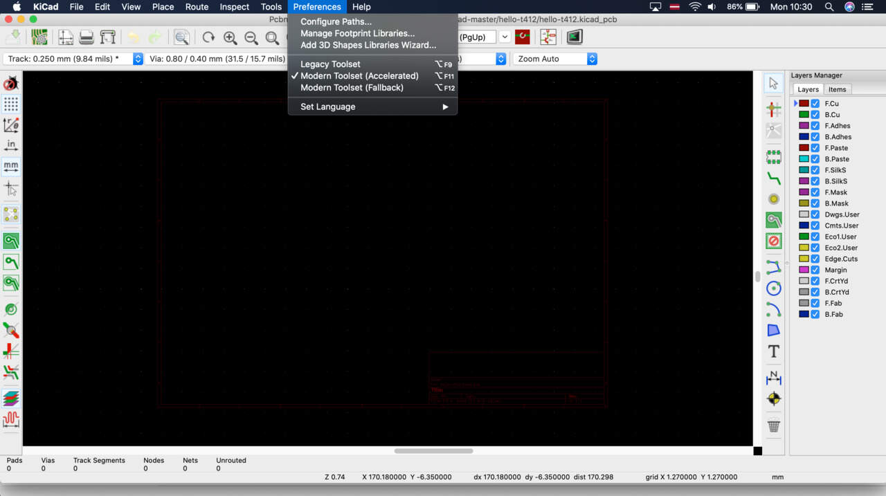
- When I opened PCB Editor it was empty, also after I clicked on the update PCB button. As I work with MacOS there are the different settings and to fix this issue I just need click on the Preferences and choose Modern Toolset (Accelareted).
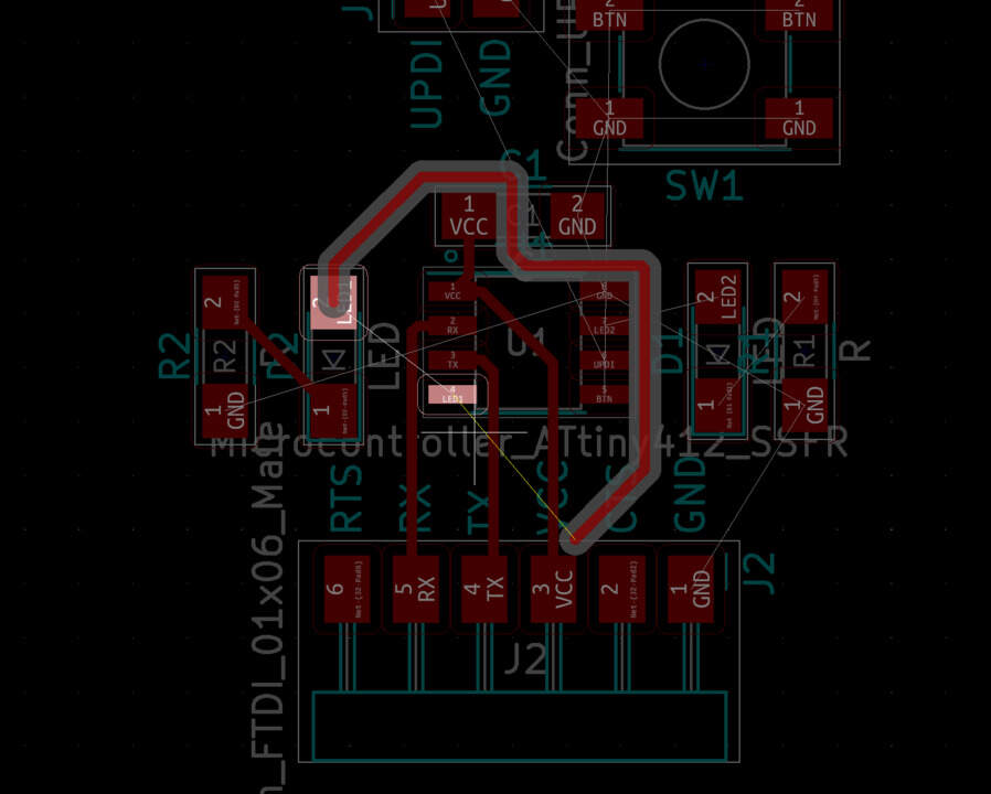
- For move parts select one of pads and hit M and then you can start moving it around. For rotation hit R.
- Usually put the microcontroller somewhere in the center.
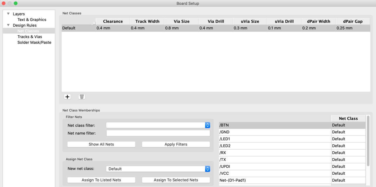
❗ Put the capacitor as close as possible. - Next is to use the root track tool in order to route the copper wires in between them, but before - it is important to make sure that you have the track widths set right and for PCB milling I want the tracks to be a bit thicker than 0.250 mm and for that click on the Edit pre-defined sizes and click on the Net Classes item and Clearance specify to 0.4 - this is the average tool size what I use for milling the PCB. Track width - 0.4 mm.
- So many times when I think that I finished my design in the last step - when I just need to connect GND, I conclude that someone GND is trapped. That some parts are trapped happened many - many - many times!
- Actually GND pins I connected later, but in this step I can foresee that later I would have a problem with GND connection.
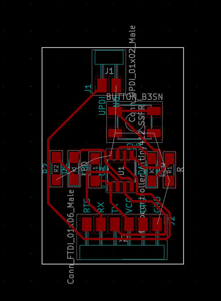
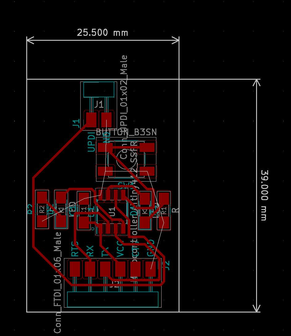
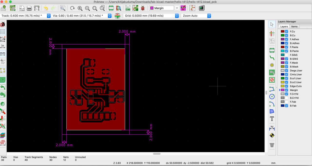
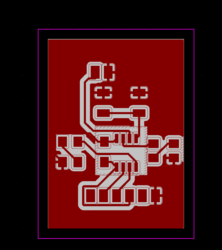
- After connection all parts (except GND) I drew an outline of the board with Graphic lines tool. Then I checked the size of the board, for that I use Measurement tool.
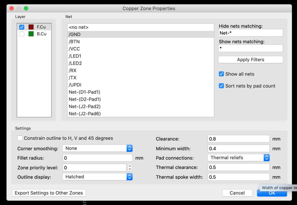
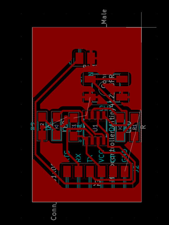
- For GND I use the Filled zones tool - check that you're in the F.Cu(PgUp) layer. As I want that fill to represent the ground Net I want to connect all the unconnected grounds together copper fill. Then specify Clearance as 0.8 mm, Minimum width - 0.4 mm, Thermal Clearance - 0.5 mm.
- Now all GND are connected.
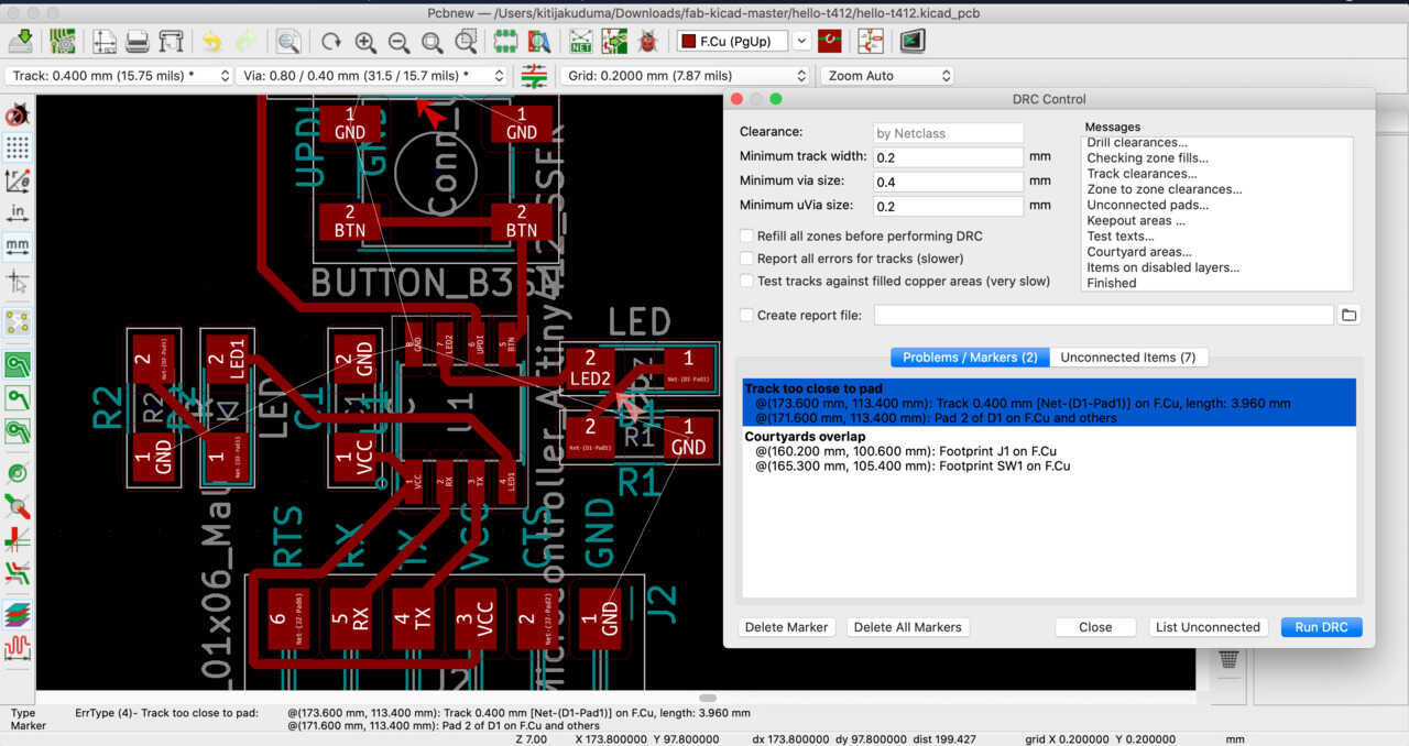
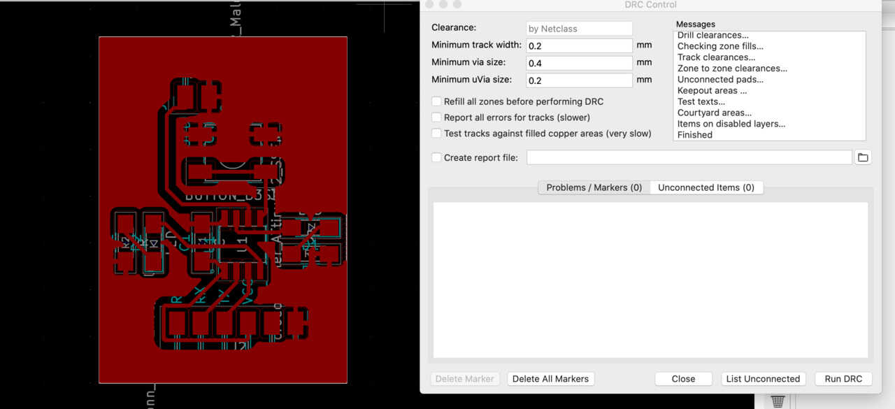
- It is important to check from time to time bugs, for that click on the Bug button and fix issues.
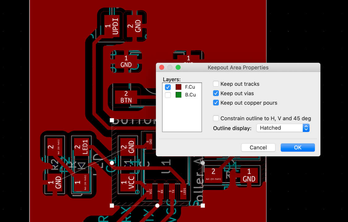
- As I don't want GND near the chips to be connected to GND directly. For that use the Keep out areas button and specify areas where the copper shouldn't appear at all. When the area is drawn, press B to process start.
- All names of elements move to the inside somewhere in the board area.
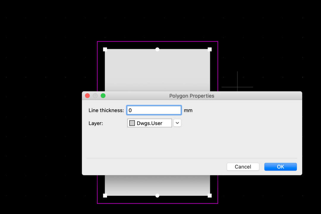
- In the Margin layer select Polygon tool, switch over to the grid of 0.5 mm and add 2 mm margin around. But I need a filled rectangle and for that switch over to the Dwgs.User layer and select Add graphic polygon - draw overboard so then I have filled polygon. For correct size of board press E for edit and change Line thickness - 0 mm.
- Now, it's ready - you can see how it looks when I started and this is the result.
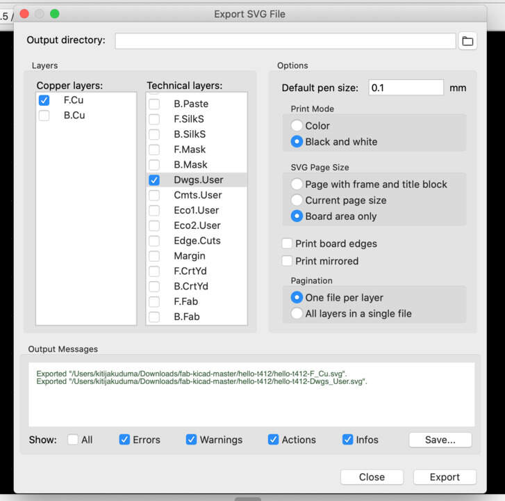
- Export it to an SVG file.
PROBLEM SOLVED!
STEP 5 : MODS
OHM'S LAW NEEDS TO BE KNOWN: LED RESISTANCE
-
❗Be careful - this section has been updated after PCB development. It is concluded that the value of the resistor used was not previously justified, 80Ω should be used instead of 1kΩ.
- Since in the laboratory there is not resistor with the calculated value the closest resistor value that I should have used based on the electronic components available in the laboratory would be - 100Ω.
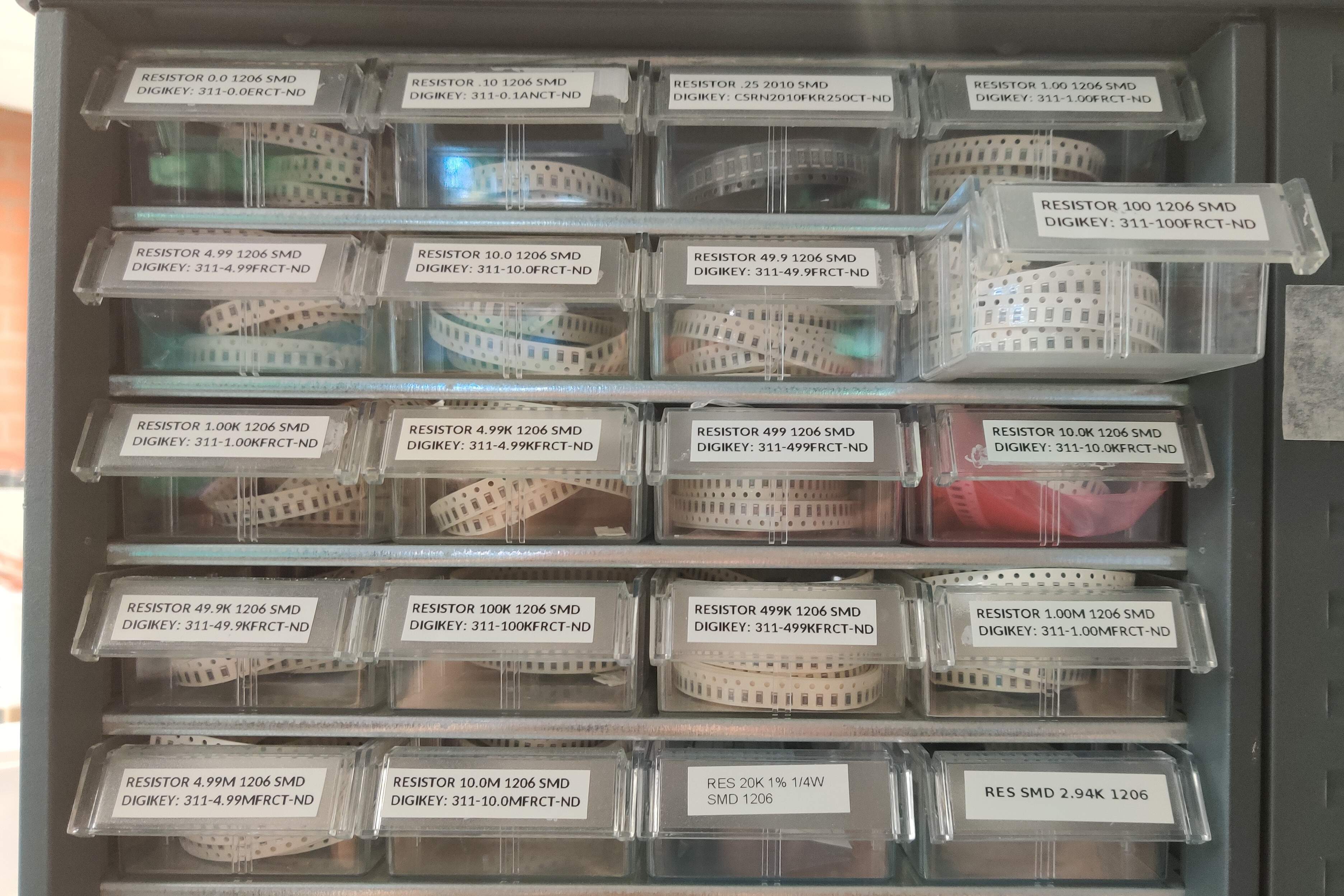
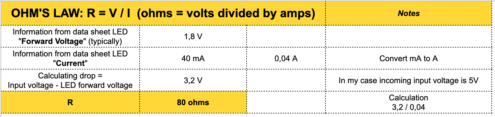
- For calculations I used - LED data sheet, convertor from ampere to milliampere, convertor from kiloohm to ohm and finally I checked the calculations in the online calculator.
SOLDERING PART
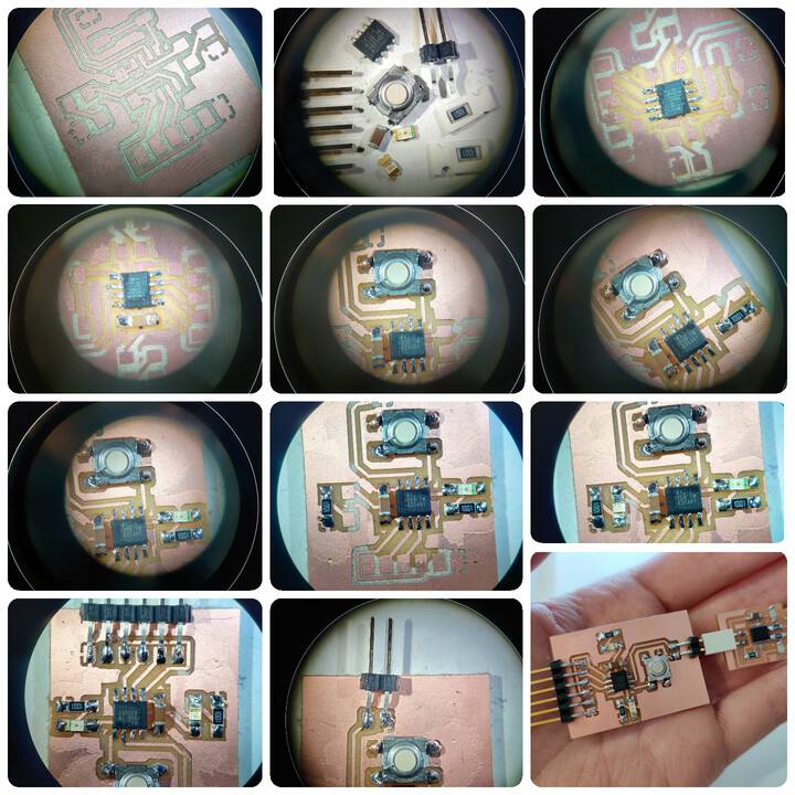
- I soldered these components:
1 x ATtiny412
1 x Capacitor, 1uF
1 x Button
2 x Resistors (for LEDS),1K
2 x PINS (for FTDI)
6 x PINS (for external power)
1 x red LED
1 x blue LED
TESTING PART
- When I tested my board for the first time I concluded that programmable is only one (RED) LED. I conclude that the (BLUE) LED I didn't add in the right direction, then I re-solder it and rotate it to another direction. And as I conclude that my previous week UPDI connection part is too small when I try it put to USB Adapter. For that I solder the USB connector. For the second test I was ready to check all functionality - it's working!
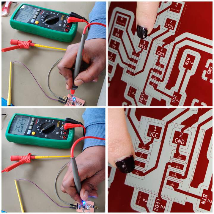
- MULTIMETER & CONTINUITY TEST
- To check how good I soldered every electronic component I did a continuity test. I use the multimeter to verify the continuity of the tracks. I looked at the scheme and tested the parts which need to be connected. In this part most beautiful is when you can hear the signal - connection is (where it should be)! I checked also VCC and LED voltage.
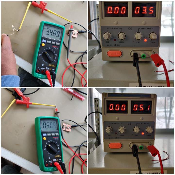
- POWER SUPPLY
- In this step I just check voltage as for the board is needed 5V.
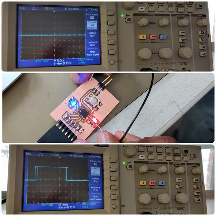
- OSCILLOSCOPE
- Ohh.. This is so complicated - I felt like in hospital, where I looked at an electrocardiogram. The biggest achievement was checking the LED signal. In the picture you can see the result when I touched it and when I didn't.