ELECTRONICS PRODUCTION
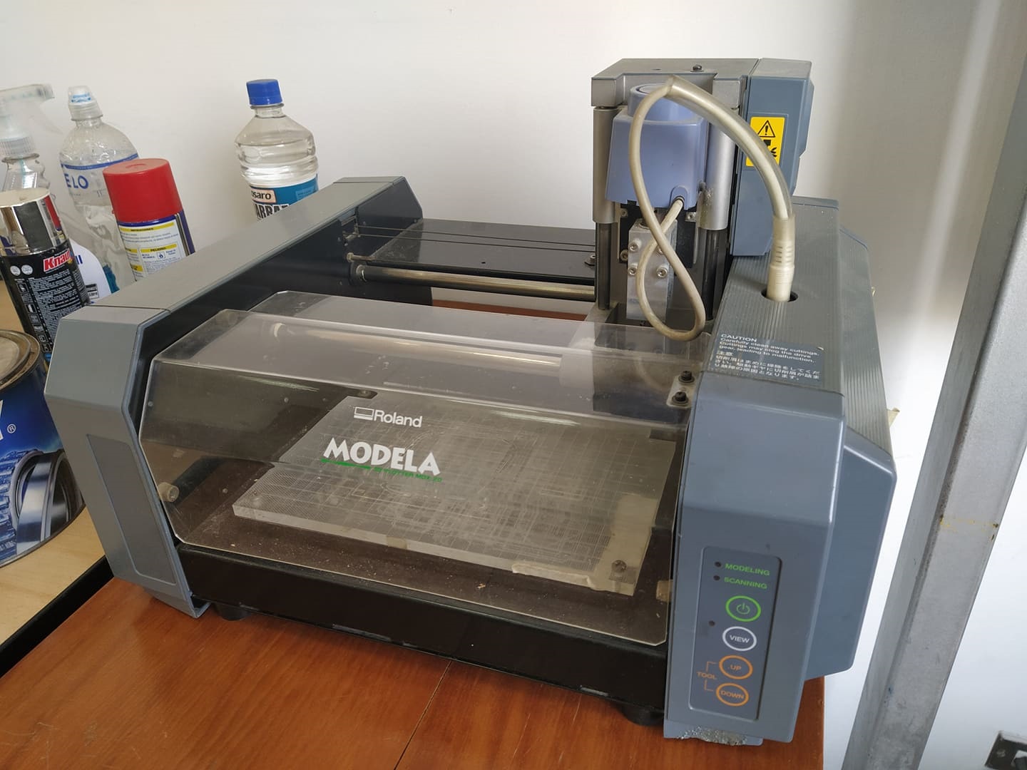
This week I worked on the characterization of the milling machine modelaw mdx-20 3D to make the programmer FAB ISP44.
Use of mods
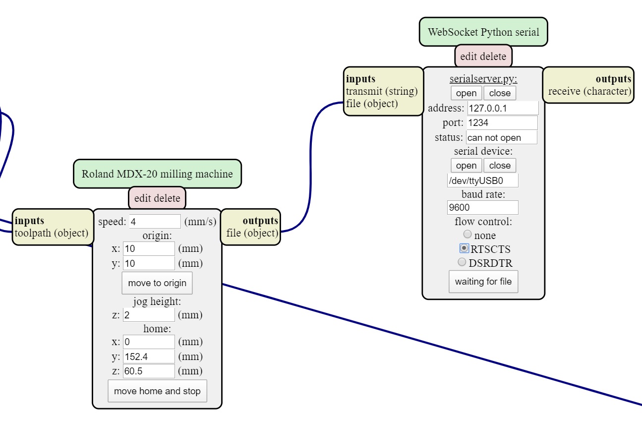
We follow the instructions shown in the image to select the machine and the task it should work with.
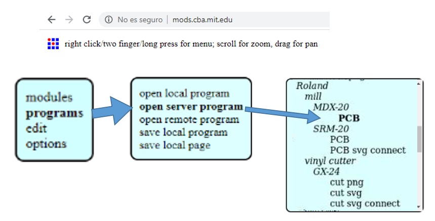
Once entered it will show us the configuration environment.
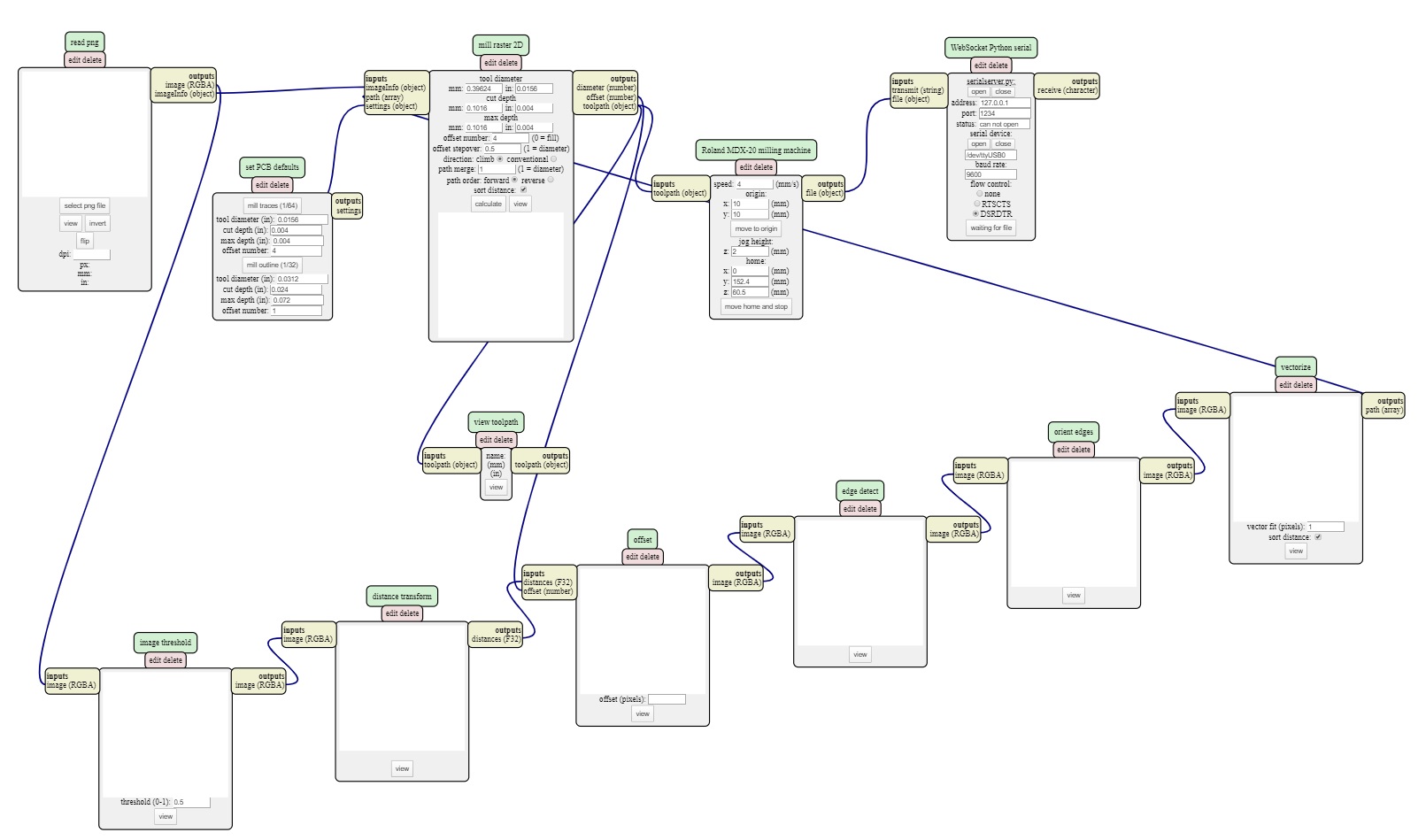
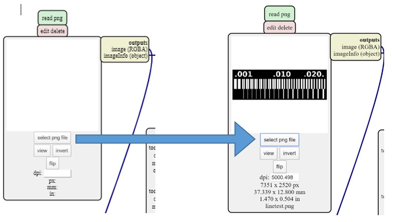
The first thing we did was select an image in PNG format because the JPG format is a compressed format and does not have a good resolution to do the job.
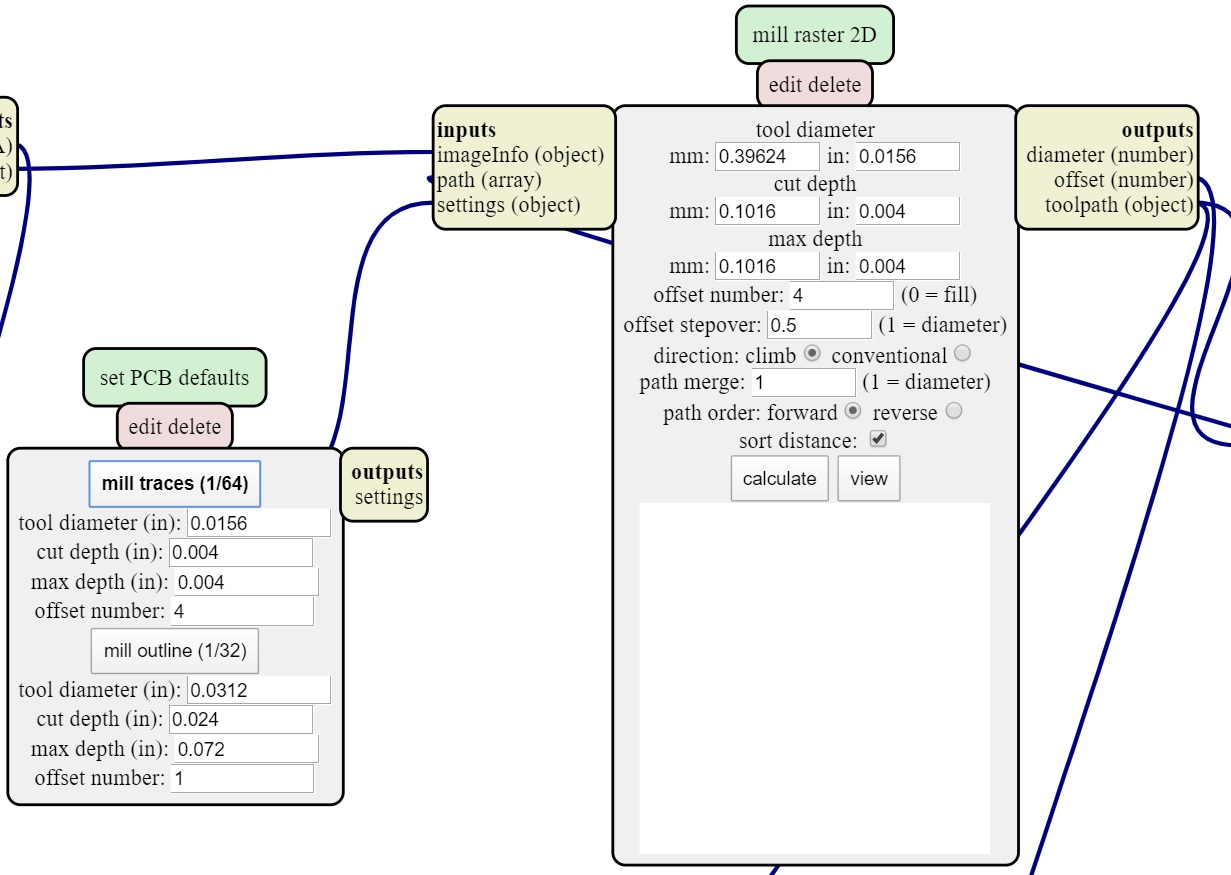
Before starting to generate the milling path, we must have parameters, such as the measurement of the milling cutter that, by default, looks like 1/64 (to trace the pcb) and 1/32 (to cut the circuit board). offset number: Here you can change how much copper you want to removes of your traces. This parameter works very well by default using 4 to do traces and 1 for cutting. Choosing 0 as an offset you tell to the machine to remove all the copper except the traces, but you extend considerably the machining time.
In parameters X and Y, we can move the machine's point of origin, in addition to calibrating the Z position of the mill. In "status" we can see if the machine is connected or not; besides being able to send the file of trajectory by means of a button in the inferior part.
By clicking on the calculate button, we can see a preview of the milling path in addition to useful information that may interest us.
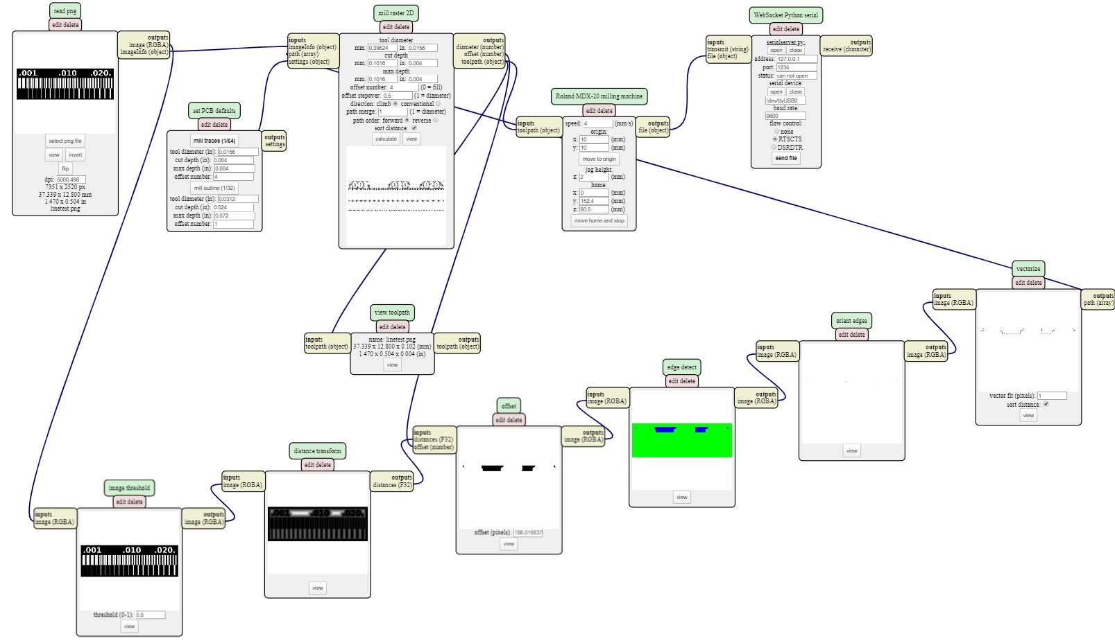
To perform the work of cutting the PCB, a .png file must be entered with the appropriate measures in addition to selecting the 1/32 milling cutter (although in our case we use the 3/32 and 1/16 milling cutter) in addition to making the cut safe of the entry pcb in the "cut depth" parameter -> "in = 0.07" to ensure an adequate cut.
In the machine we will find 4 buttons, which are defined by their color: green-on; white-sight (to move the plate forward); orange-to define the position on the Z axis of the machine (it must be quite precise to give an adequate position).
To fix the copper plate, use double-sided spruce tape (preferably covering the entire bottom surface to ensure that it is level).
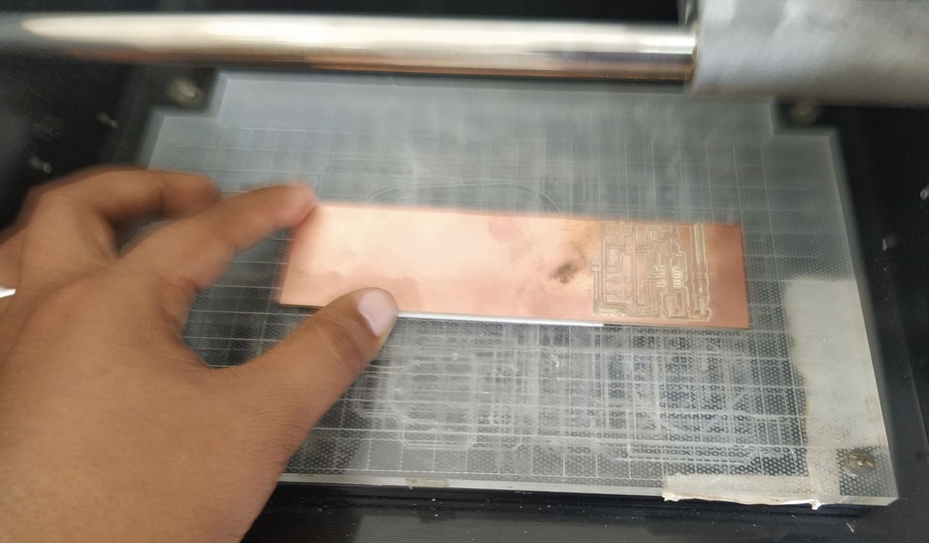
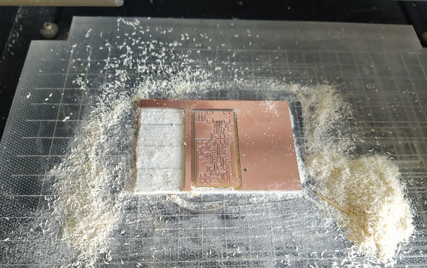
I started with the milling tests using 1/64 milling cutters and for cutting a 3/32 cutter, (at the time of the most complicated start it was to square correctly the Z-position of the cutter, because if it is located too low below can release too much copper from the plate).
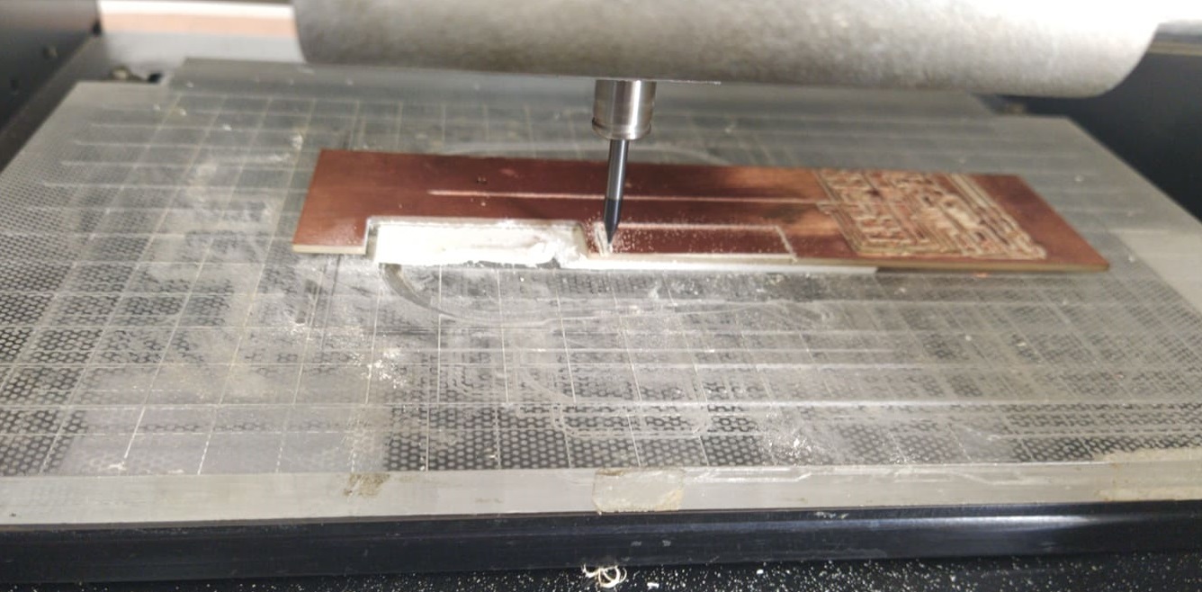
Here I show the first result of milling both cutting and tracing. where a detachment of collection can be observed due to a bad location in the Z axis and milling of the milling cutter.
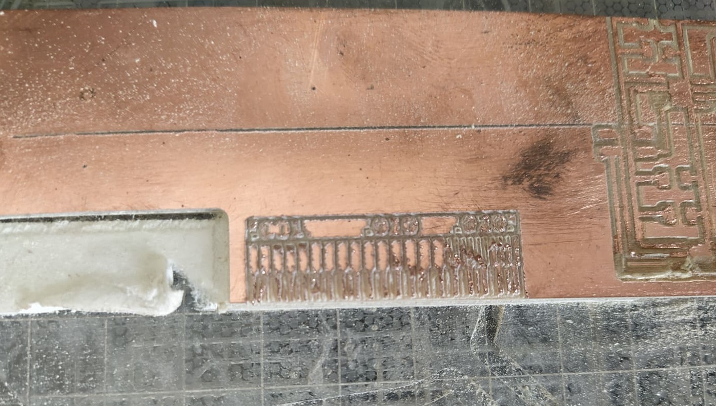
Continue to carry out more tests until I can be guided by the sound of the cutter when coming into contact with the copper in order to define a suitable position in Z, achieving a better result both in the trace and in the cut. In addition to identifying that the thickness of the copper tracks must be greater than .015
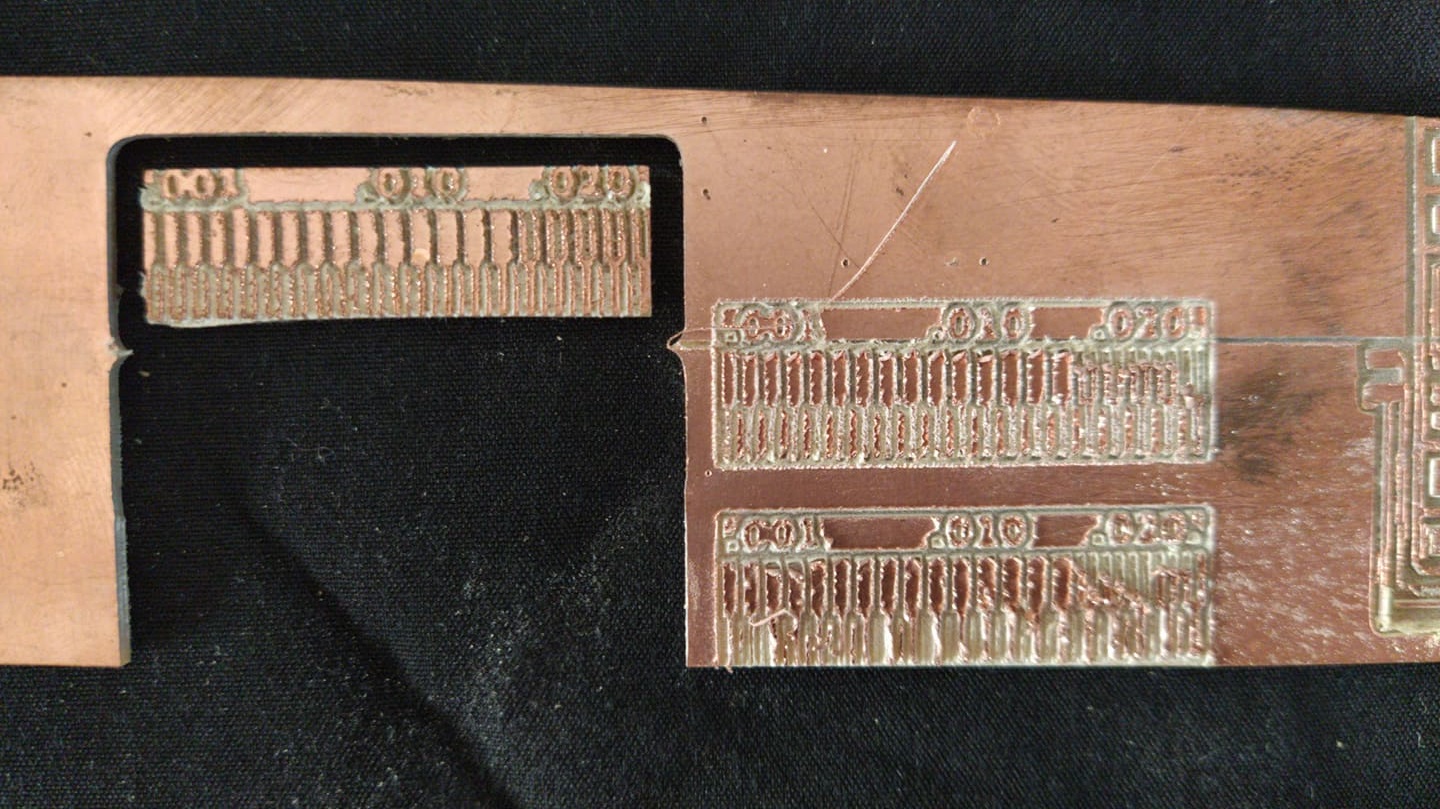
I proceeded to trace the circuit for the ISP44 in which I had to use a 1/16 milling cutter because the 3/32 cutter came to damage the circuit on the sides.
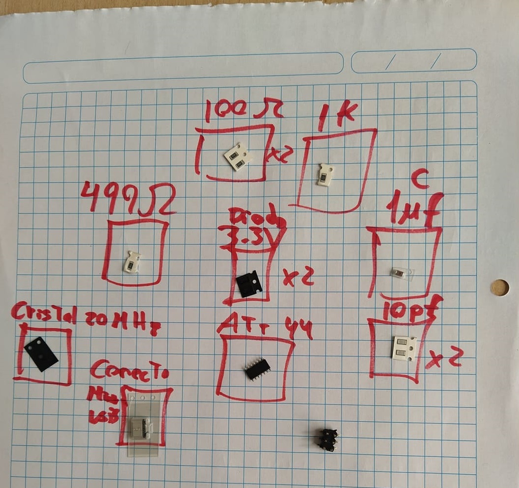
After properly sanding the circuit, I proceeded to gather the necessary electronic components.
To perform the welding process use, a clamp, a press, a soldering iron, tin and flux
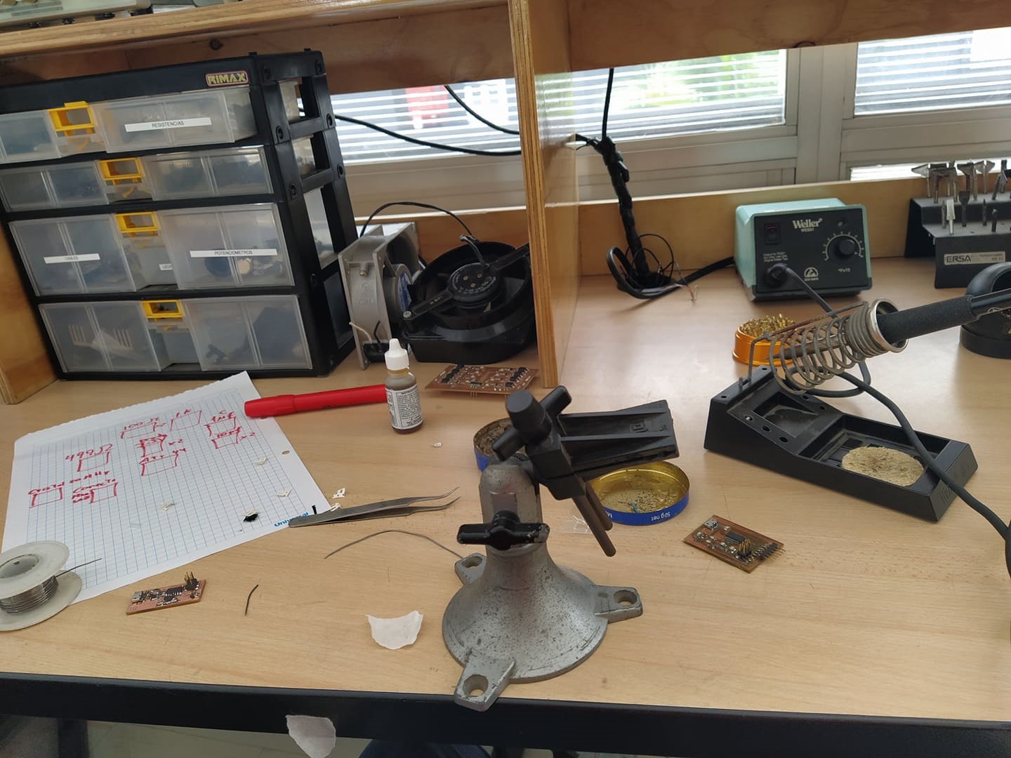
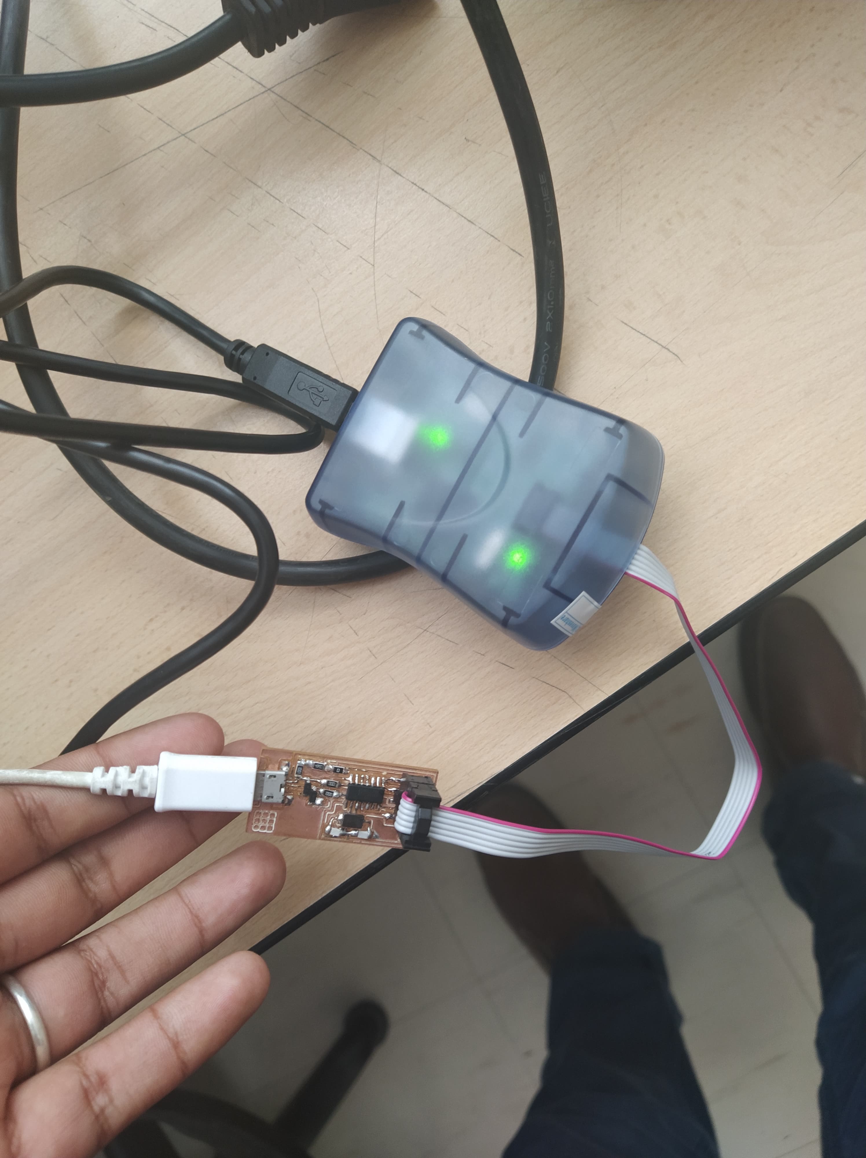
Giving me the following result; where the most complicated thing was to solder the micro usb port and hold the smd components.
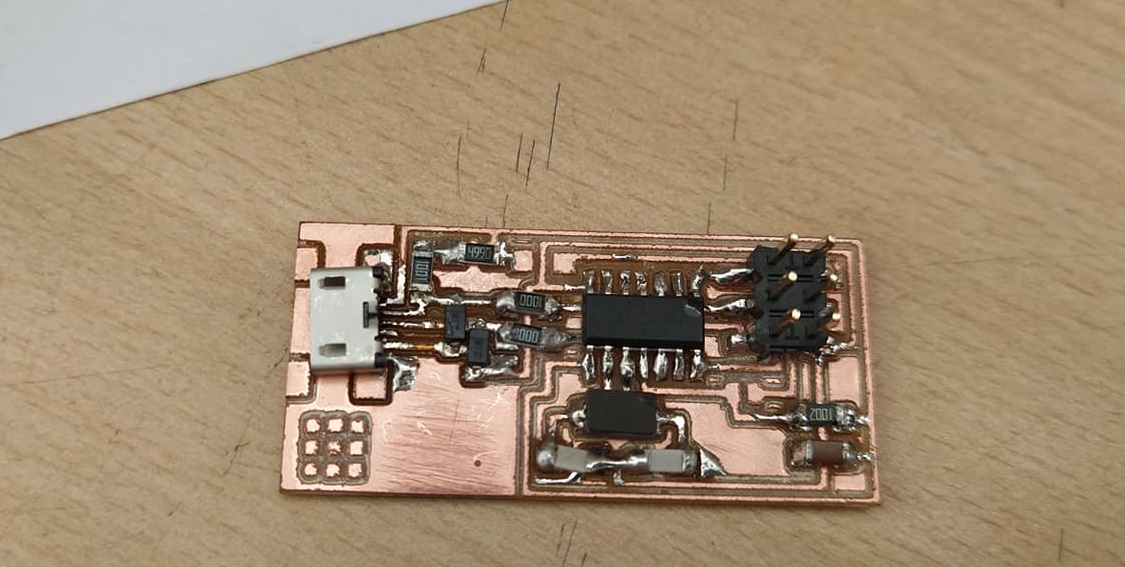
After finishing the circuit, perform continuity tests to verify that there is no short circuit. additionally weld a resistance of 0 ohms to temporarily connect the "SJ1 and SJ2" to be able to program it; When I connected it to the computer, I verified that there was no short circuit and that the welding was successful.
Self evaluation
What problems did I have?
I had problems with the programming because some computer with Linux was not available to be able to program, in addition to it I find it difficult to make the code.
How did I resolve the problems?
A specialist was called so that he could enable one of the computers and be able to carry out the programming.
What should I improve?
I must improve my programming skills, by welding I must improve my technique to give a better finish to my projects.