
A7
Electronics design
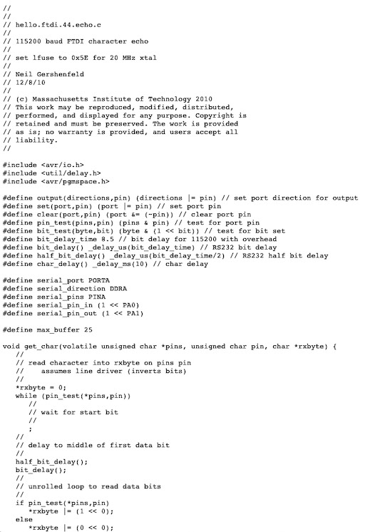
Following the electronic device learning, we reached the simple and straight-forward thinking process of designing an electronic board, following precise directons to emulate / rethink an echo -hello world- board: hello.ftdi.44, to understand how this device works and test how the energy frequincies pass throgh it to ensure a self-working micro-device.
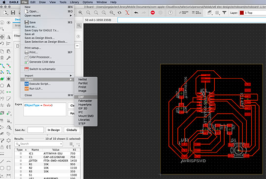
We started using a new software: EAGLE recently aquired by Autodesk, that has a very large array of options for designing electronic boards, from simple to complex, form 1 sided- to even some layers.

So, first, as a local assignment we needed to redraw and re-trace an existing board, to understand the program, the inner process and how to export to a PNG file.
The process is quite simple, once you get familiarized with the libraries and components, because there is such a large list of blocks and pieces.
Most of them are commercially found and are listed in the inventory page from the FabLab webpage.
The idea of re-tracing, is a way to understand how to improve the already design inner "roads" in a board.
And, with that, you can set new dimensions to the finished board, rememebring to use the same components.
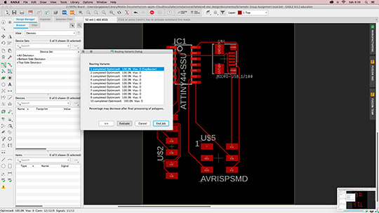
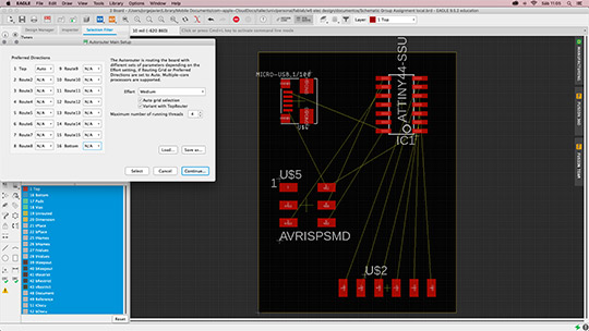
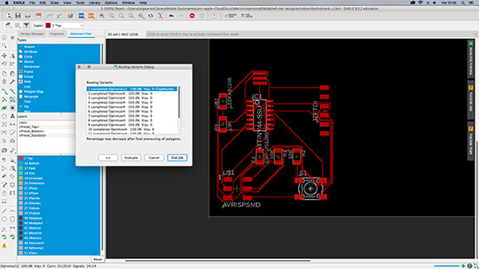
There's the option to automatically generate the traces inside the design...
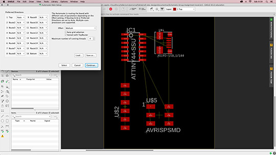
It takes the necessary steps to link and trace the board...
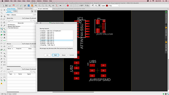
However, sometimes, the finished traces are so close together, that some finer manually actions are needed.
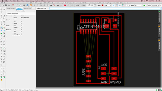
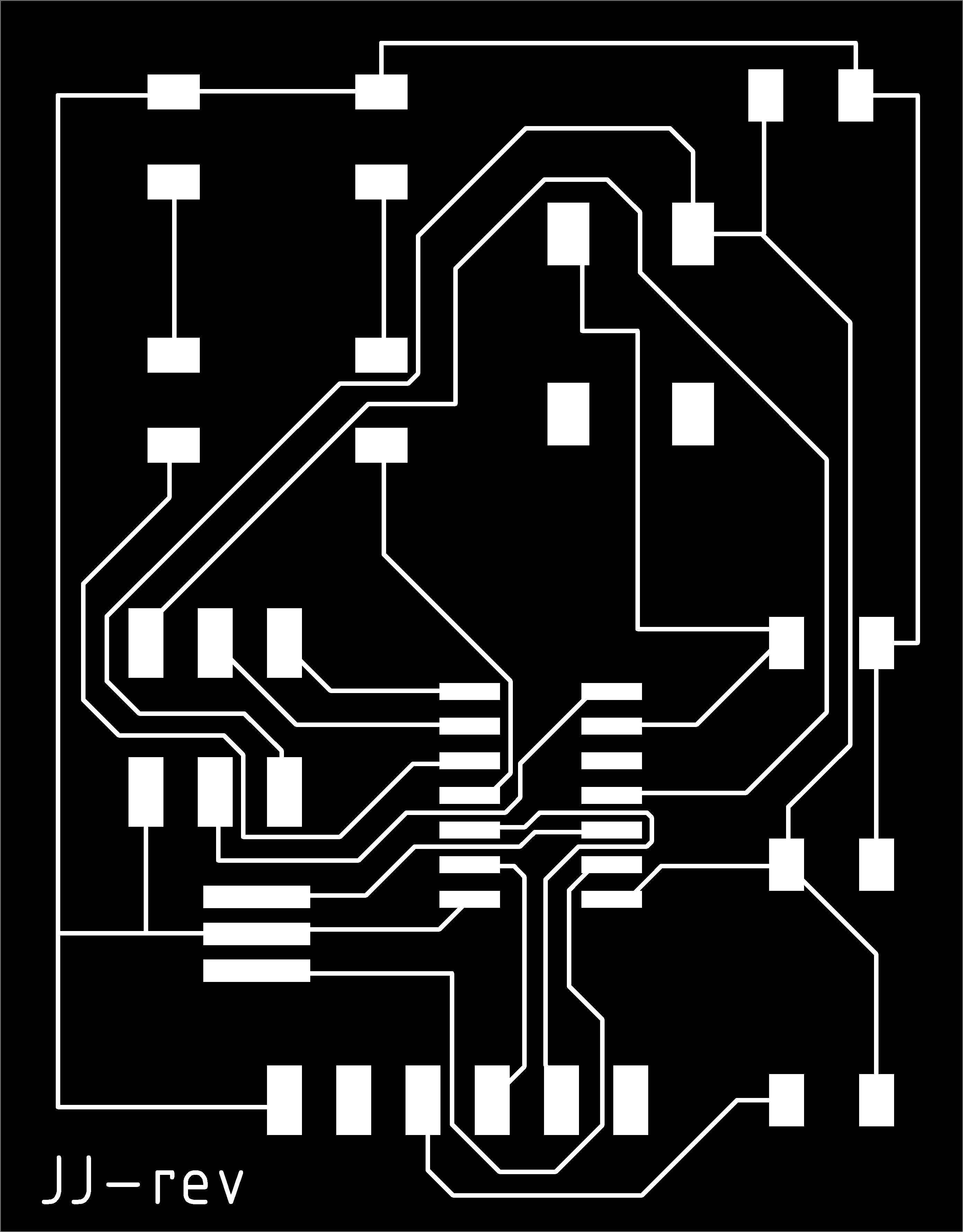
Something like this is the work-in-ptogress board.
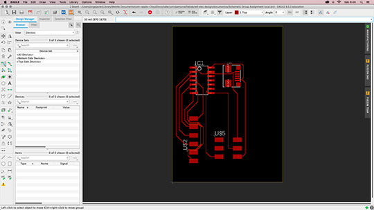
So i re-traced it following a diffrent path, and the result was a little bit better.
Creating thicker and separeted lines along a virtual grid.
Getting a desired path, leaner and easier to send for milling, a series fo 10 to 12 mil lines.
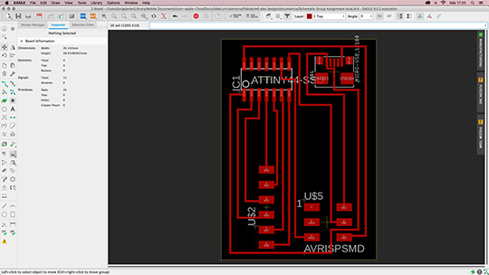
Something like this...
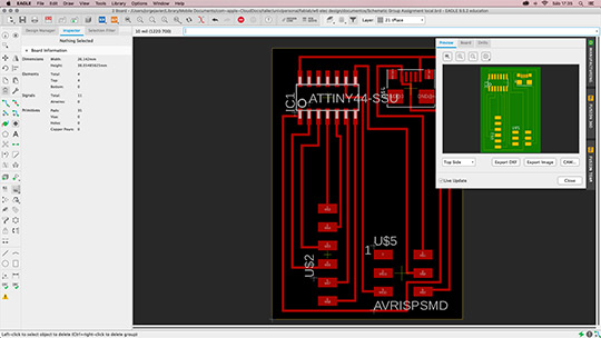
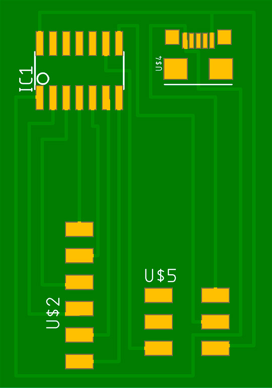
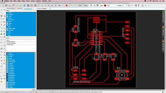
The finished traces...
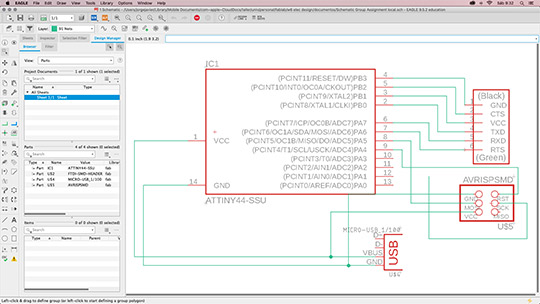
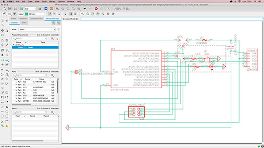
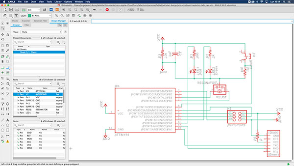
Second, i used all this new information to create a brand new board from the echo -hello world- board.
I had to follow the same design rules as we learned in the class, but search for parts that the lab have in stock.
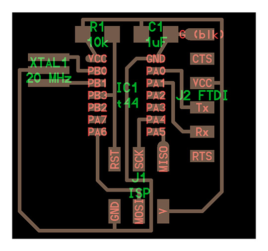
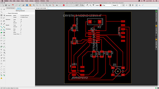
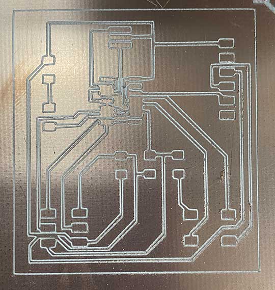
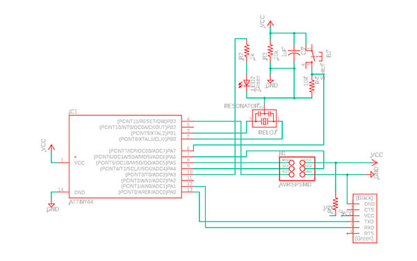
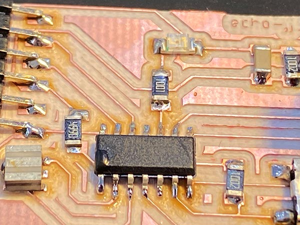
I used the image above as a guideline, following the basics to produce a reliable circuit connection. the main parts are the ATtiny 44 micro-controller, 6-pin connector, resistors and capacitors.
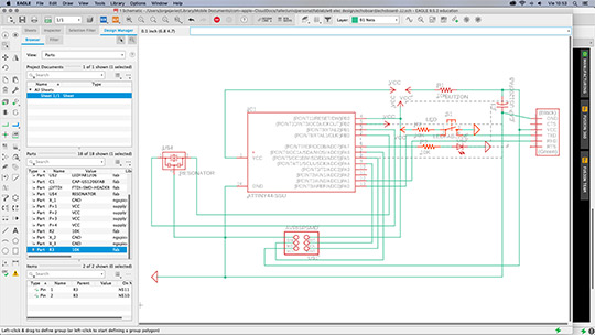
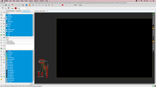
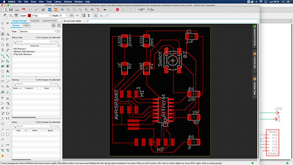
Once sent to the board setup window, i created automatically the traces.
i used 6mil thinkness traces, beacuse of the very close lines around themselves.
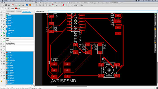
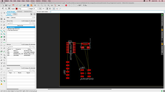
i checked twice that the traces wouldn't touch each other, and then i re-arranged the inner design.
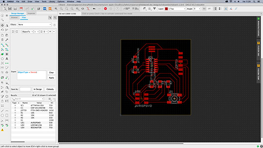
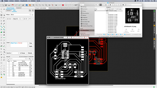
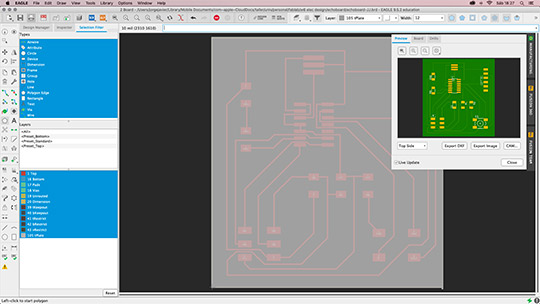
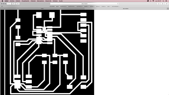
Then i exported the traces as png monochromatic file.
The finished image.
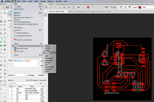
As an option, i exported as dxf file.
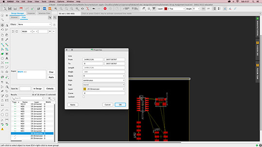
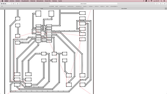
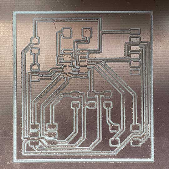
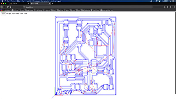
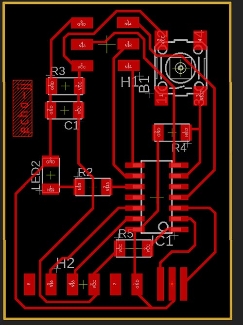
And then, the revised version with manually traced lines, creating better paths along the square.
the external trace for finishing while sending to milling.
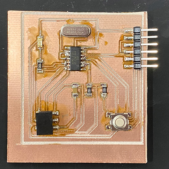
A second revised version using a non-grounded crystal capacitor.
The finished traces ready to be exported as png file.
The mods process for milling and evaluate the traces.
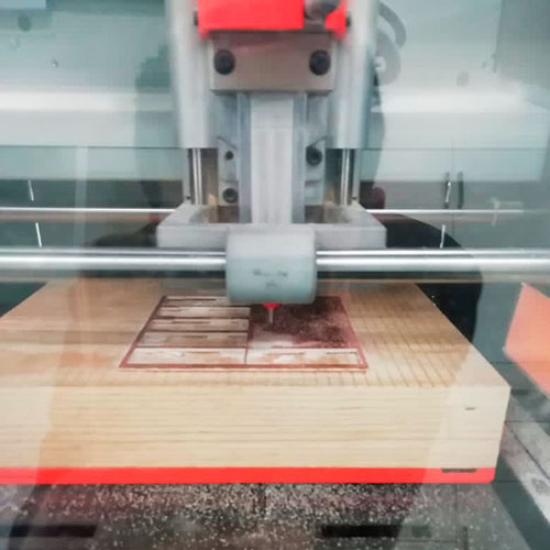
The process with an offset milling of 3 passes.
The setup, second revision to be sent to milling.
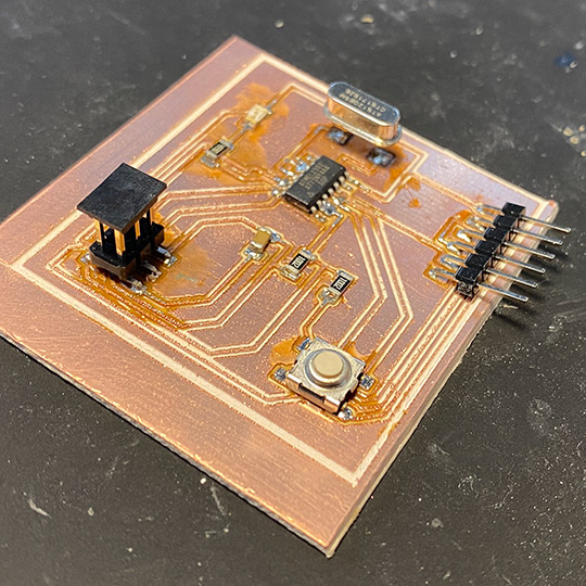
First attempt.
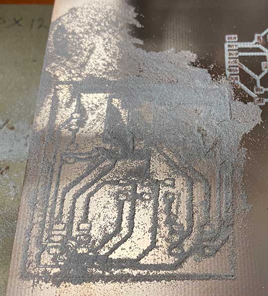
Finished board with some mistakes... the connections below the Attiny44 are cramped altogether.
Second attempt with the ungrounded crystal device and better milling process.
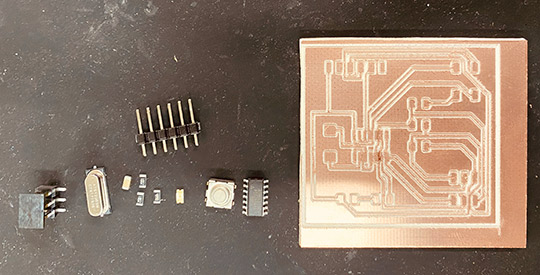
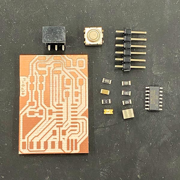
Components:
Attiny 44
Crystal
10k resitors
499 resitors
traslucent LED 2k
Button
10k Capacitor
Conectors
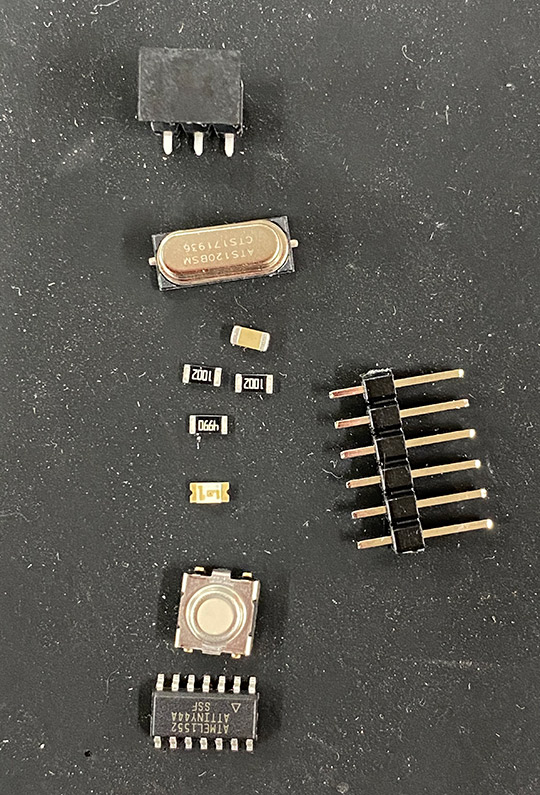
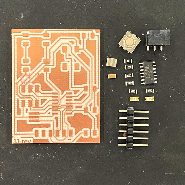
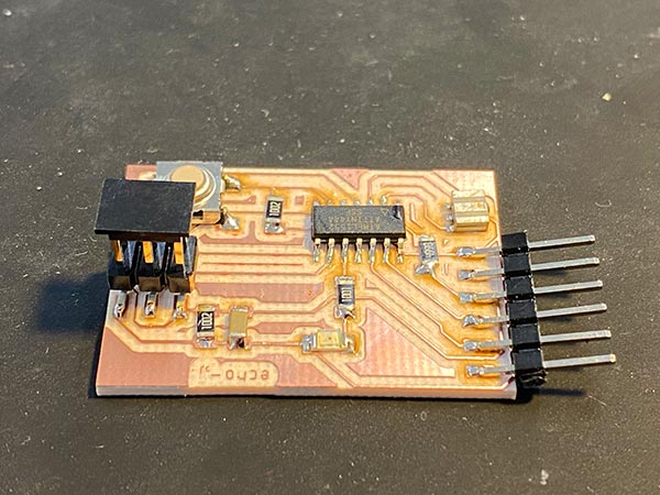
The whole set
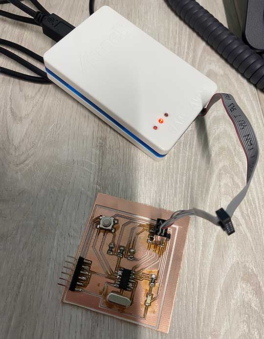
Soldering...
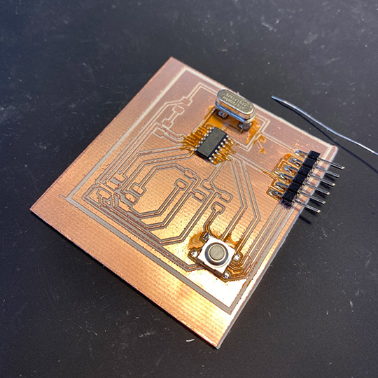
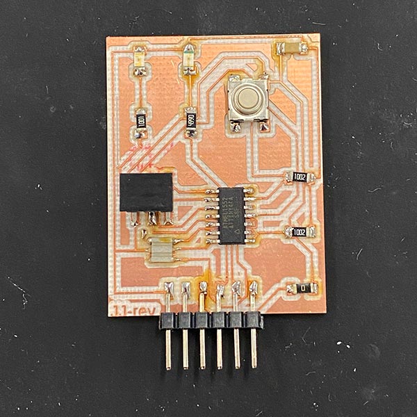
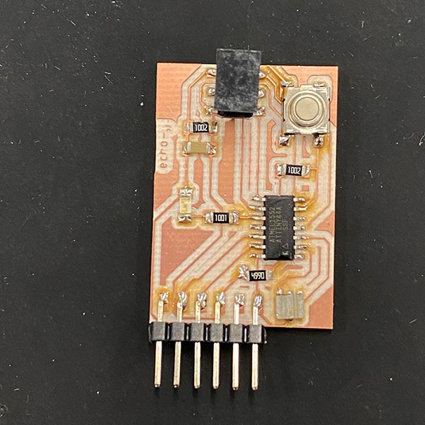
wide view of the finished echo board
Finished echo board
Programming... and almost there...
Doing it all over again...
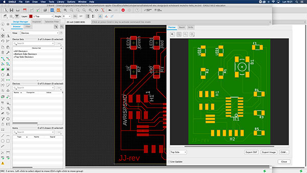
After using our new FabLab space, i decided to give it a try again with a similar PCB board, using two LED, green and red.
Redrawing with a little bit os patience, getting all the traces following a certain "logical" path
Then, checking connectivity as well as certain common errors as vias merging.
Second attempt with modproject, sending this new board to the Roland mill, with 4 offset passes and a 1/32 milling bit
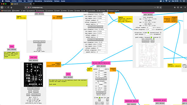
The printing process sharing the board to match our common tasks.
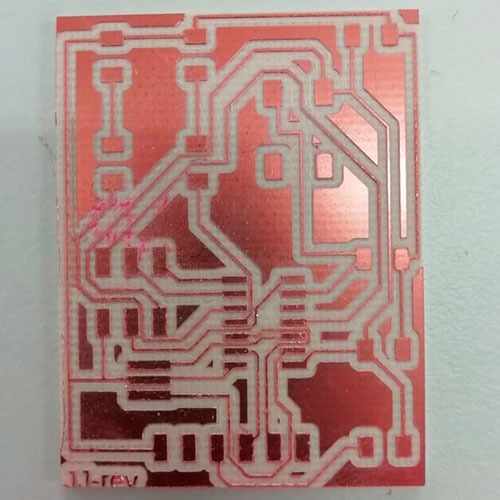
A new PCB board with quite thin traces but better milled than before.
Now, i used the next components:
-ATTiny44 processor
-AVR programmer
-Resonator
-LED green clear
-LED red clear
-FTDI header 6 pin
-Capacitor 1uf
-6mm switch
-resistor 0
-resistor 10k (x2)
-resistor 490
-resistor 1k
i soldered everything trying to used as less material as it could be to have clean connections, figuring out that i created a very open pcb board.
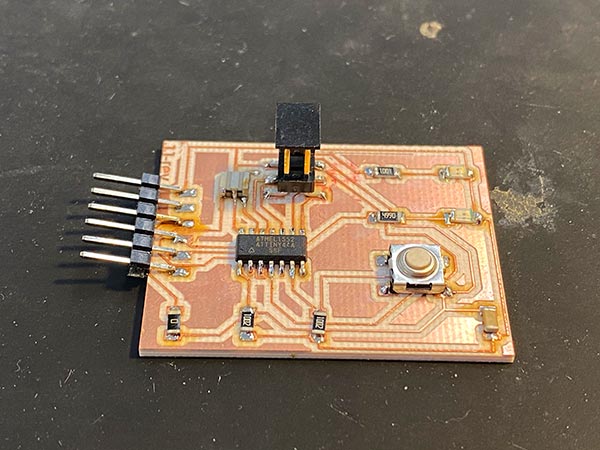
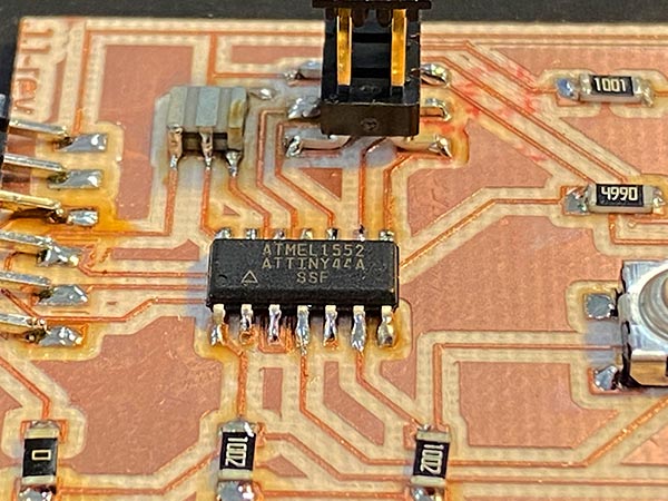
By testing its connectivity and overall electrical flow, i'm in the process of debuging it.
I wanted to try a compact pcb, optimizing the components and the space bewteen them, to have less space and a smaller board.
Most of all, i wanted to have a better serial with the VCC and GND routes.
(i was dealing a lot with those conecctions)
Again, i used these components:
-ATTiny44 processor
-AVR programmer
-Resonator
-LED green clear
-FTDI header 6 pin
-Capacitor 1uf
-6mm switch
-resistor 10k (x2)
-resistor 490
-resistor 1k
So, the new challange is to fit everything in a smaller size board, finding that ensuring the soldering process, i actually can achieve a better result.
Again, i tested connectivity and electrical flow... waiting ti be debugged.
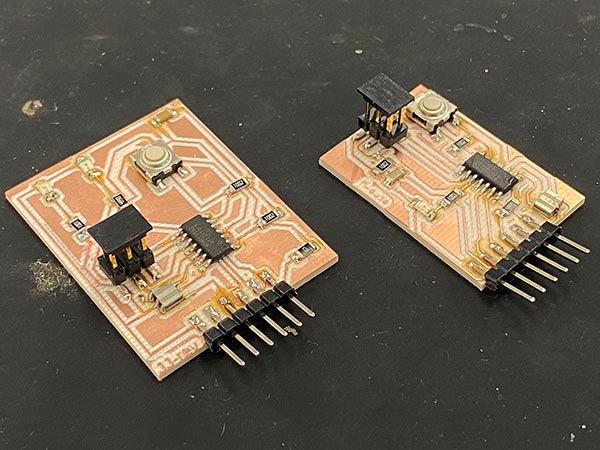
Comparission of the boards.
At least for me, this process has been very enlightening, throughout this weeks i have understood the importance of electronic design, and how i need to focus on the pieces to ensure an improved piece.
