WEEK-4: ELECTRONICS PRODUCTION
This week we focused in electronics side of the course with PCB fabrication. i.e fabricate our own ISP (In-System Programmer).
This week Assignments are:-
- Individual Assignment - Mill a programmer circuit and Solder the components
- Group Assignment - Learn in detail about milling PCB and the machine used in our lab, its parts, parameters, tools used etc. & Mill a test using the given diagram
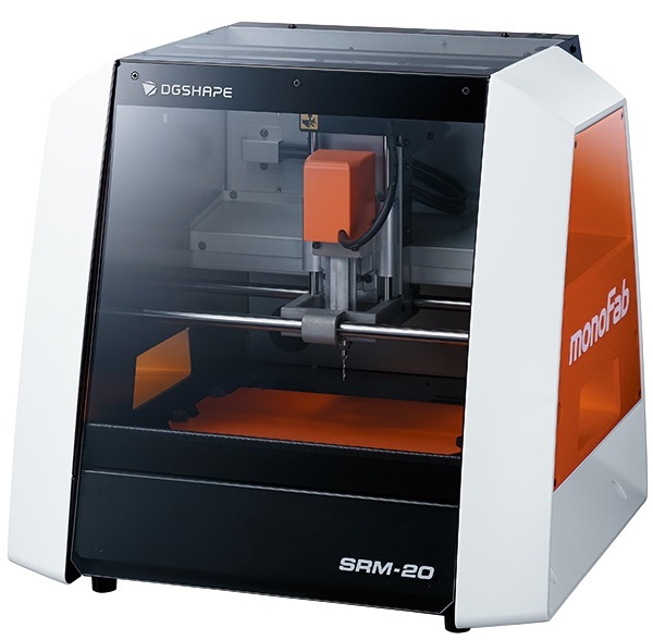
Milling Machine:-
Our lab was equipped with monoFab DGSHAPE SRM20 model milling machine.
Bits used for milling:-
This machine has 2 milling bit. One as tracebit for tracing the circuit in board (i.e 1/64) and another one as cut bit for cut the board(i.e 1/32)
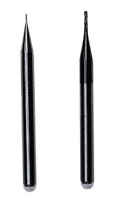
The bit on the left is 1/64 and the bit on the right is 1/32
The SRM-20’s VPanel controller provides a simple interface for adjusting tool position and moving the cursor to set the milling starting point.
The VPanel also allows easy control of feed rate and spindle speed with pause and resume operation, plus tracking of X, Y, Z axis milling with a numeric readout in millimeters or inches.
In-System-Programmer(ISP):-
The ISP is a programmer for AVR microcontrollers, designed for production within a FabLab.It allows you to program the microcontrollers on other boards.
To do this, there are 6 main steps:
- Preparing your file.
- Preparing your machine.
- Mill your board.
- Cut your board.
- Solder components.
- Programming the board.
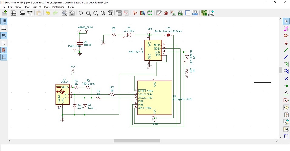
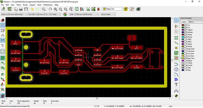
I was used KiCAD software for design the Schematic circuit and draw the PCB layout. My schematic circuit is given below:
 Once completed the schematic circuit, the following steps proceeds further for prepare the PCB layout:-
- Annotate PCB foot prints.
- Perform Electrical rule check and clear the errors.
- Assign PCB Foot Prints to the schematic. Here we can add the necessary components from the library.
- Run PCB New to layout printed circuit board.
- Here, the connections are shown in white as per out schematic circuit diagram. Further, we draw the route tracks without cross connections.
- After completion of route track add the edge cut line.
- Then add the filled zones.
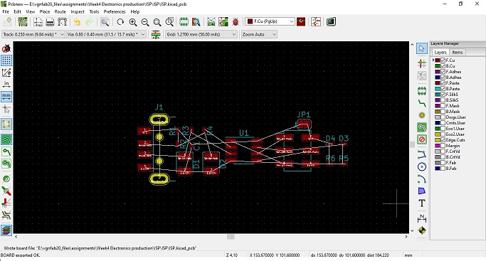
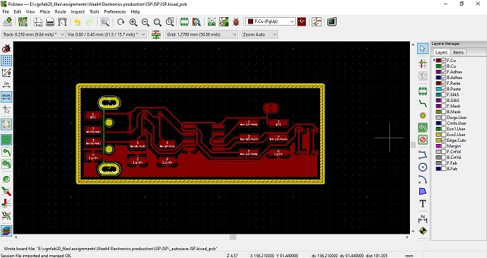
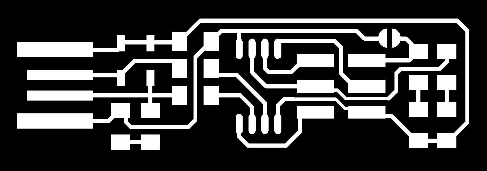
The pcb design of my In-circuit Programmer is shown in the image below:
Actually, this week assignment is not to "Design" the ISP, but use one of the "pre-defined" designs from the Fab Academy class site.
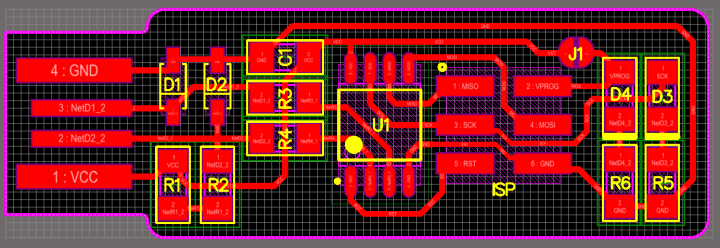
For learning purpose I have done all the above said designing. I am following Fabacademy’s FabTinyISP tutorial from the class site and using this design for making the ISP board.
The PCB layout, Trace and Cut files are given below:
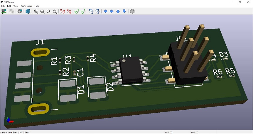
 The components of ISP board are:
- 1x ATtiny45
- 2x 1kΩ resistors
- 2x 499Ω resistors
- 2x 49Ω resistors
- 1x red LED
- 1x green LED
- 1x 100nF capacitor
- 1x 2x3 pin header