-
2013 project
Group assignment
Designing the electronics
Making the schematics
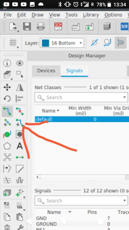
Making the board in Eagle
Making the physical board
KiCad
Extra comments on electronics design
Connecting and programming the board
Reflection on this week
Manuals and files
2013 project
There is not much to say about the 2013 project except for this was the week where it went all to 'hell'. It was the first week that I couldn't finish back in Iceland. And it kept following
me for the rest of the academy. I was prepared for a hard week, hoping that this time it would go better than last time.
What went wrong in 2013? Libraries can be very overwhelming for someone that never worked with them. Though, on that point I got help back then. Where I didn't get help were the
stages after that. Finishing up the schematic, and making the actual board in eagle.
Group assignment
For the Group assignment this week we looked at how the electronics measurement tools work. This includes multi-meters but also more complex tools like oscilloscopes. Our findings can be found here, on our group project page. However, as I'm a partly remote student, I took the oscilloscope from my own lab and ran the same tests as they did in Brussels.
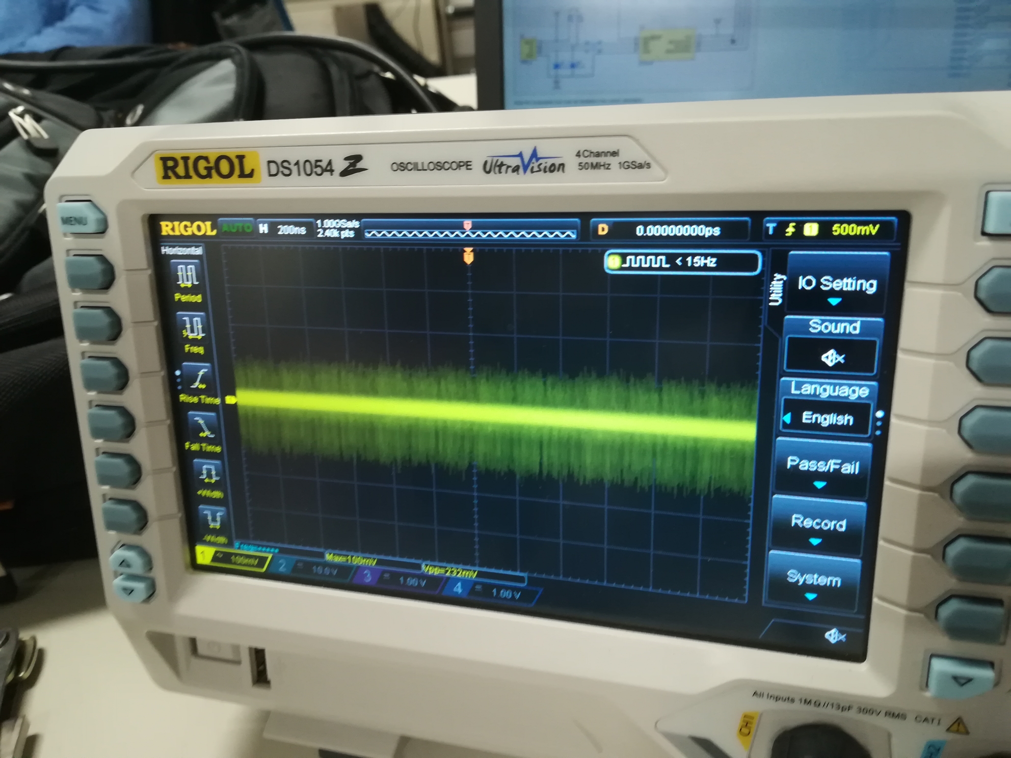 Noise when booting up the scope.
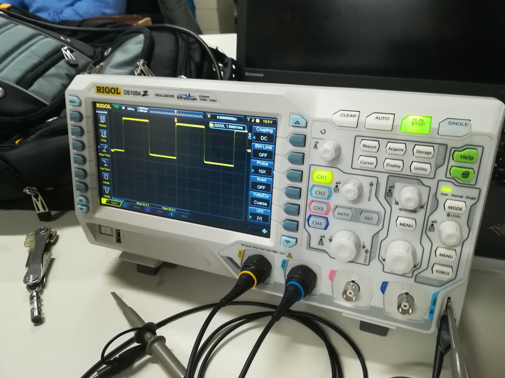 Trigger voltage position vs 0V signal reference.
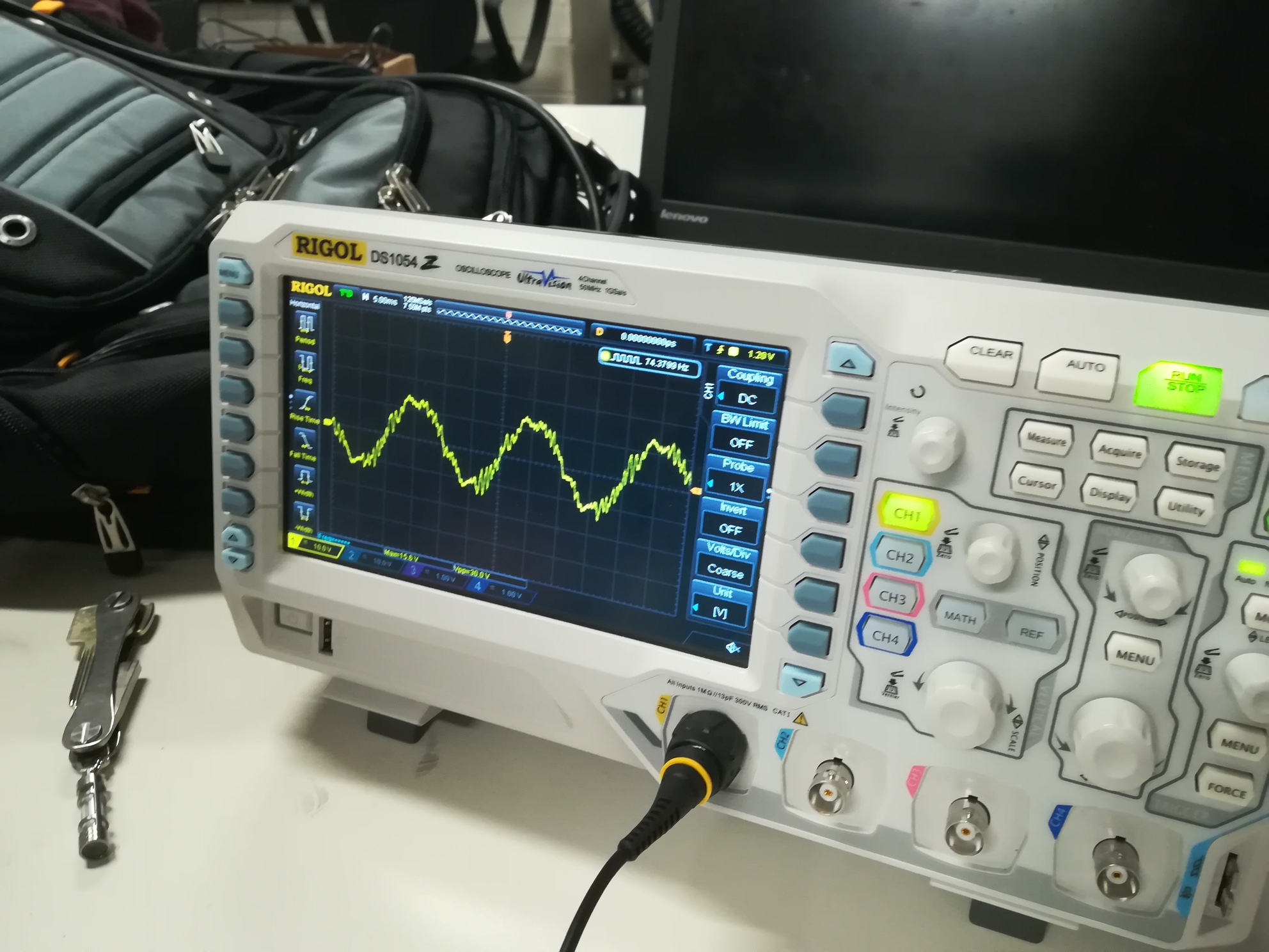 A detailed view of the graph time / voltage on the oscilloscope.
Another interesting link on the subject that I found, was here: How to use a scope. It explains the basics and gives you an intro to all the terminology.
Designing the electronics
I was prepared for this week. This was the week where everything went to hell in 2013. I was going to do better than back then. Full of good motivation, I installed both Eagle and KiCad.
Changes in our workflow at work made it possible to start drawing in KiCad, but I didn't get far and did decide to start with Eagle instead.
To top
Making the schematics
First things first: making the schematic. At least something was still hanging around in my head from 2013, and that was how to import a library into Eagle. In no time I had it up and running and could start making my first sketches. But nothing ever goes as easy as planned. Just like when we had to make our ISP, I was overwhelmed by the numbers and letters that components carry. And as usual I wanted to run before I could walk. Without even having finished my first, easy, board, I was already asking questions about adding text and supply's. But I found that more interesting than trying to find the right components in a sea - sorry library - of components.
It turns out, to make things easy, that you can just take an R for resistor. You can just the basic one and later add the value to it. And a LED for a LED. The only thing I cared about was that the footprint was a look a like and that my micro controller was correct. Before this point of figuring this out, I got a bit panicked and called in the help of Abdon. Most of the pictures that follow are screenshots from his side to help me figure out Eagle and PCB design.
Problems I ran into while making a schematic:
- What is it with all those components?
- Help! My component is not in the library!
- Numbers
- Supply's
- Adding text
As said before, the first time you dive into a library in Eagle, it can be quite overwhelming. There are 100ds of resistors, capacitors, LED's... Of course it all depends on the formula and values, as you might need a stronger or lesser component. Still, it's overwhelming!
It can happen that you want to use a component that is not specified in any libraries that you have (standard eagle or FabLib). You could go online and search for a library that has the specific part. Or you can look at footprints and add those to your drawing. In my case, I needed to use a ATtiny85, but there was none in my known libraries. I stressed a bit about it until Abdon told me to just use the ATtiny45 as they have the same footprint.
As we know from the ISP week, numbers are not my forte. So my question here is: why does an ATtiny45 have 8 pins while an ATtiny44 has 14. Apparently a higher number in the name doesn't mean more pins.
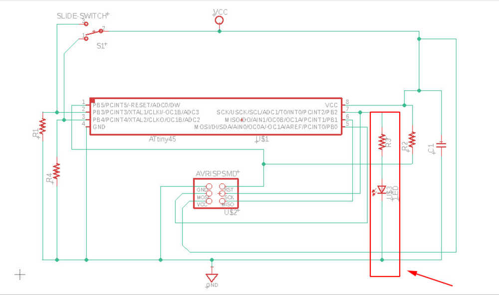
As I struggled with the hello_world board from the FabAcademy, I turned my attention the the board that I'll be redesigning for my final project. In the end, they both look very similar. Same kind of micro controller, lots of lights as output, and a switch/button as input. It went better than with the FabAcademy board, as it was more straight forward. But the schematic that I used to copy the board of looked... different. My work makes use of 'supply's. It means that you're not drawing every line in you schematic, but you use symbols like 'ground' or 'vcc' to connect one line to another. I saw it a bit as 'portal'. Current will from from one component to another, then it disappears, only to show up again somewhere else in your schematic.
Something that drew my attention in the LedUp Kidz file was that some lines had text.
I started modifying another file by adding LED's. The questions rose: how, what, where? At this point, datasheets are important as you need to know the voltage that runs through one pin and calculate how many LED's can be powered on one pin. Turned out that, for the thing that I wanted to do, I could just copy and paste LED's and resistors.
Update end of March 2019: the first thing that you have to do is not making the schematic but figuring out WHAT you want the board to do. For now we're only talking about LED's and
buttons, but it will change pretty fast to sensors and more complex components.
Second to that: write down all the necessary components so that you have a checklist of what you need to make the board.
To top
Making the board in Eagle.
Armed with a working schematic, I started exploring the board section in Eagle.
I followed the Autodesk tutorial that I mentioned above and started getting frustrated by how slow everything was going. Long live WhatsApp, because again Abdon showed me some important
functions in Eagle that I should know off.
The auto-command can be found in the middle of all other icons and is - honestly - not very visible. After Abdon pointed it out to me I started using this one. Always happy that my
results were okay and wired.
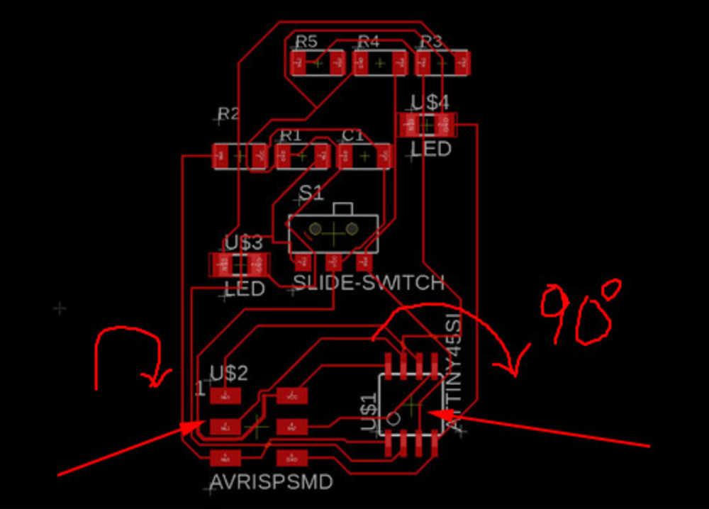
As I started drawing my own lines after using the auto command, I sometimes needed to change the traces, but didn't always see the solution. A second opinion is always handy then.
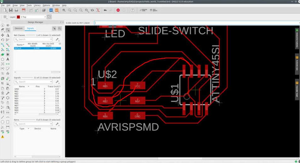
Sometimes you also need to try different orientations of your components. This alone can solve a lot of problems.
To top
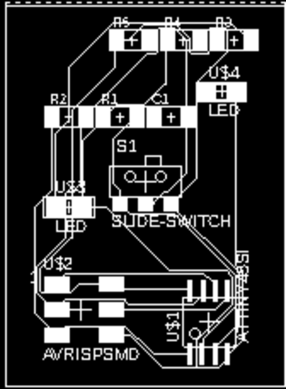
Making the physical board
Once I had my traces and my .png image, It was time to make my own board. But not before running into trouble.
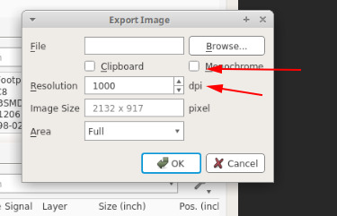
The first thing I had to overcome was exporting. I looked for the options: .png, .jp(e)g, ... But didn't find it. Eagle however has the function but calls it: image. With that solved
I exported my first .png, but didn't get what I wanted.
- The text, and values were in the way
- It was reversed. Though I already know how to fix this.
My favorite method of making the board is using the vinyl cutter. I tried cutting the board, but it resulted in weird lines and lines that were to thin.

Standard the lines in Eagle are on 0.006 or 0.012. I changed this to 0.016 but it didn't help when cutting the board. I started playing around with the width of the lines, keeping in mind
that they cannot touch each other. We did find a solution in Eagle, but it's painstaking as I need to select every trace apart. Selecting all the traces and then going to properties,
changing the line with does not work.
How did I do it?
- Step 1: make the schematic
- Step 2: make the board
- Step 3: find your trace that you want to change
Right click on the trace -> properties -> width.
You can change the with there, or up in the screen if you don't go to properties.
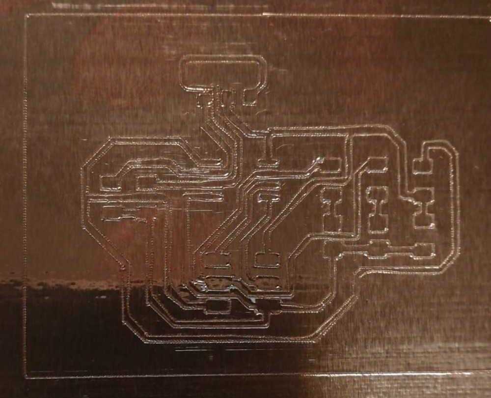
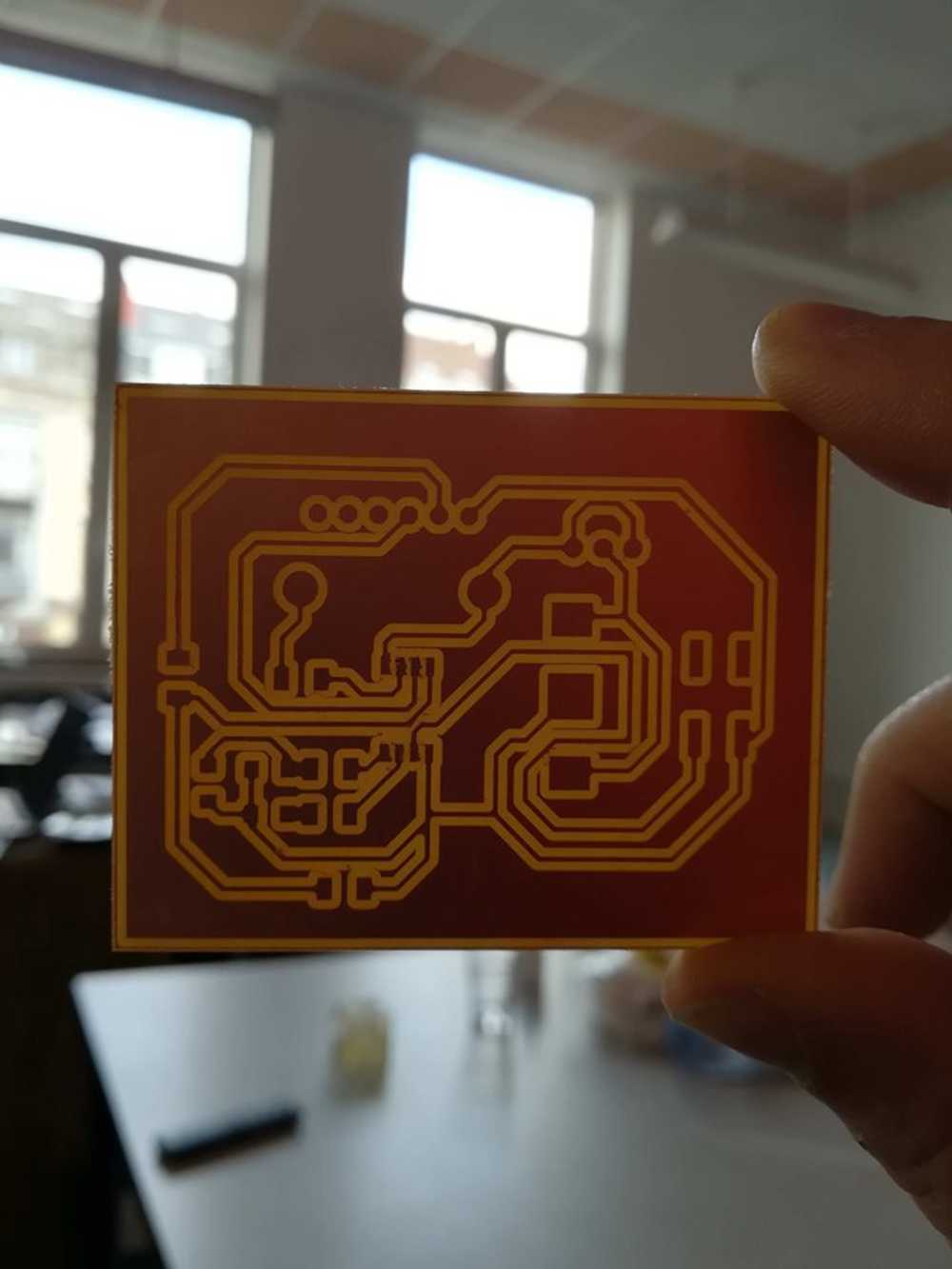
Eventually I went with another solution. I need to edit my .png in Inkscape as the Brother Scan 'n Cut can only read .svg files. While changing the bitmap to vector, I also increased the
stroke style. Normally there is no stroke and only fill. Because of adding the stroke, we get thicker traces, next to that I also put my stroke to a path. This results in lines inside and
outside of my drawing. After taking out the fill, I could see those clearly. Adding the break apart command makes it possible to take out the inside of the drawing. Leaving me with wider traces
to cut out on the plotter.
I tried to plot out the circuit now and got a perfect result.
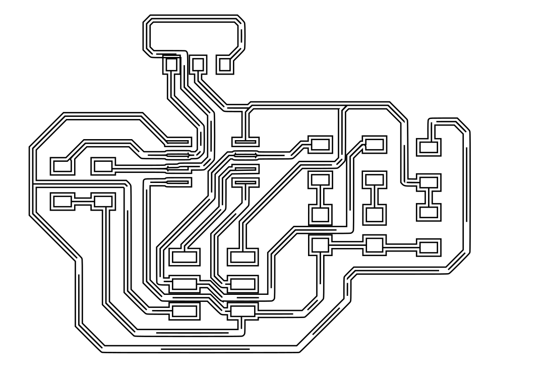
 Lines before tracing from Eagle image
 Lines after tracing from Eagle
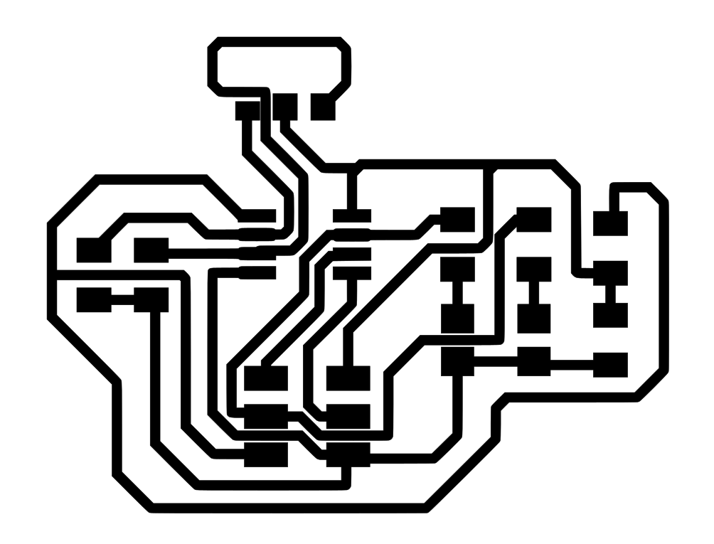
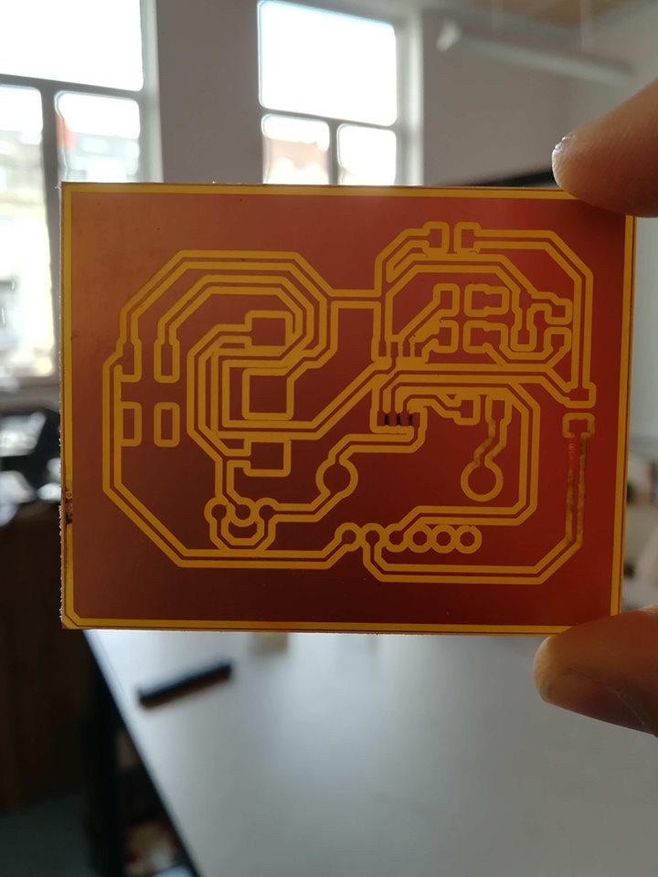
 Lines cleaned up
 Lines with fill.
 Lines vinyl cutted
KiCad
I did try working in KiCad, but sadly never got further than trying to import a library. I asked help to a friend who uses KiCad for work in the hope that he might be able to help. When asking my question to him, he started laughing and told me that's one of the more "not easy" things in KiCad. But we can import libraries from Github/gitlab even though even that is still a hassle. We're going to take a look at it next week.
It was the ULB lab and Christophe that helped me further with KiCad and the import of the library. But as I already got started in Eagle, and found (or didn't find) my way around in that program I decided to stick to one program for now. KiCad won't run away and I'll have plenty of time in my newly started electronic sidetrack to explore it on a later moment.
To top
Extra comments on electronics design
At some point in life you need to learn how to fly solo. And after spending time on Whatsapp, YouTube, in the ULB lab and the lab where I work, I finally managed to make my first solo PCB. It still took me 3 more drawing options and adaptations in Inkscape, but I got there! You might wonder what went wrong between Abdon and others checking my files and my actual pcb. Several things actually.
For starters, you need to include all of your components in your drawings. We're not sure how or why, but among other things I forgot the FTDI pins. I guess that I was mostly focused on adding the LED's and the button/switch that I didn't pay attention to it anymore. Once that was fixed, I printed out the circuit and started etching. Only to come to the conclusion that the xtal that we have in th ULB lab is bigger than the one Neil has. In the mean time I also learned a new thing or two about etching (keep it moving for example), but I'll leave this out of it as you can find an updated section on it in electronics production. So there I was, with a etched board and a xtal that didn't fit. I had several options to fix this. Or I imported a new xtal into my library, or I made my own footprint in Eagle, or I adapted the drawing in Inkscape. As I only needed to split 2 lines, I chose for the latter. 5 minutes later I had my new circuit traces and could start etching and soldering again.
Connecting and programming the board
Once the board was etched and soldered, I tried to connect it to the FTDI cable and connect it to the computer. At first, the burn-test worked fine and I was happy that non of my components started smoking. I moved on to the next step, to find the USB in my list of ports, but didn't find it with the 'lsusb' command. I decided to change the connections to the FTDI cable and try again. This time however there was smoke coming out of my micro controller. Not exactly what you want.
I asked Benny for help and we troubleshooted the board together. I told him that it would probably be the micro controller that burned through and we used the multi meter to measure out the current that passed through the component. We ended with a 'high score' of more than 1 ampere through the micro controller. Definitely the part that burned. We also learned that one of the LED's was not working even though we checked them before.
After that we took to Eagle to check my file and where the short circuit could have happened. We ended up with a whole new "hello world" board, without bridging this time.
 Partially soldered hello world board
Another thing that changed was the way of programming the ISP. Before we worked with the ISP made in one of the previous classes. Sadly, the ISP didn't survive the trips to the FabLab, nor do I like the ftdi connectors on the boards all the time. This with my final project in mind. You can't have a necklace our little gadget with those pins on it. Therefore I changed to a Arduino as ISP, which is the same was as how we program at work. We prepared a new board for me and I was ready to go.
The main change with this is that I can't solder the micro controller to the board before programming, unless I add special patches in the pcb to do so. Another thing I learned while making this pcb is that you, when you mill it out, can see mistakes in it by keeping it in the light. As shown below.
 Lines here are all clear of shorts. (picture from final board)
 Shorts are visible near the micro controller part (picture from final board
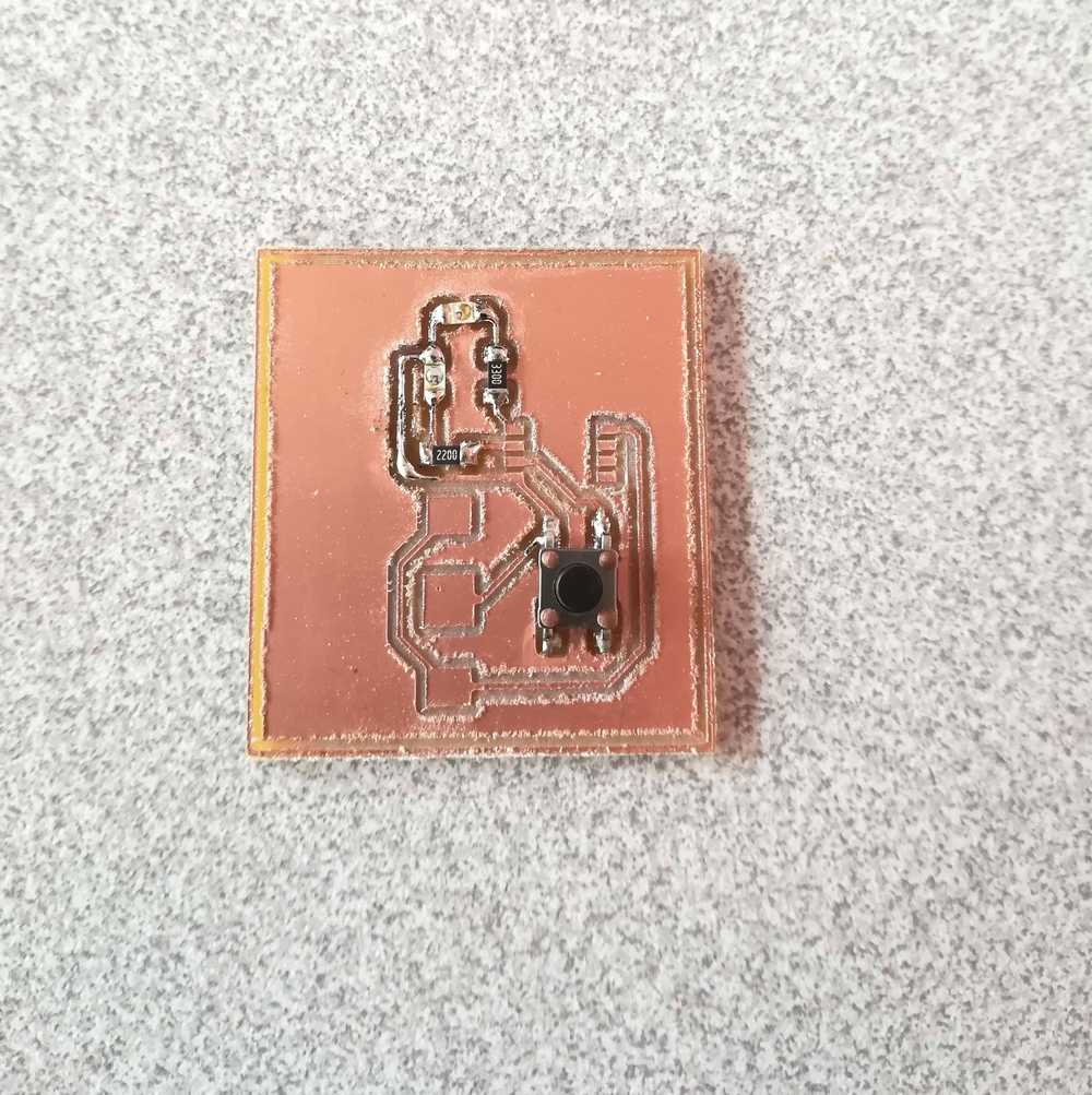
In the end we took all the mistakes out and have a working board now. When you push the button, the lights start blinking, for as long as you keep the button pushed in. For coding I used Blockly, a web interface that we use at work for the kids. The files and code can be found below. More on the programming and coding in the embedded week.
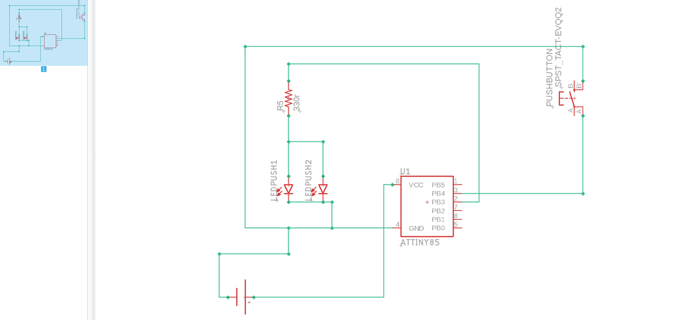 Schematic for the hello_world board
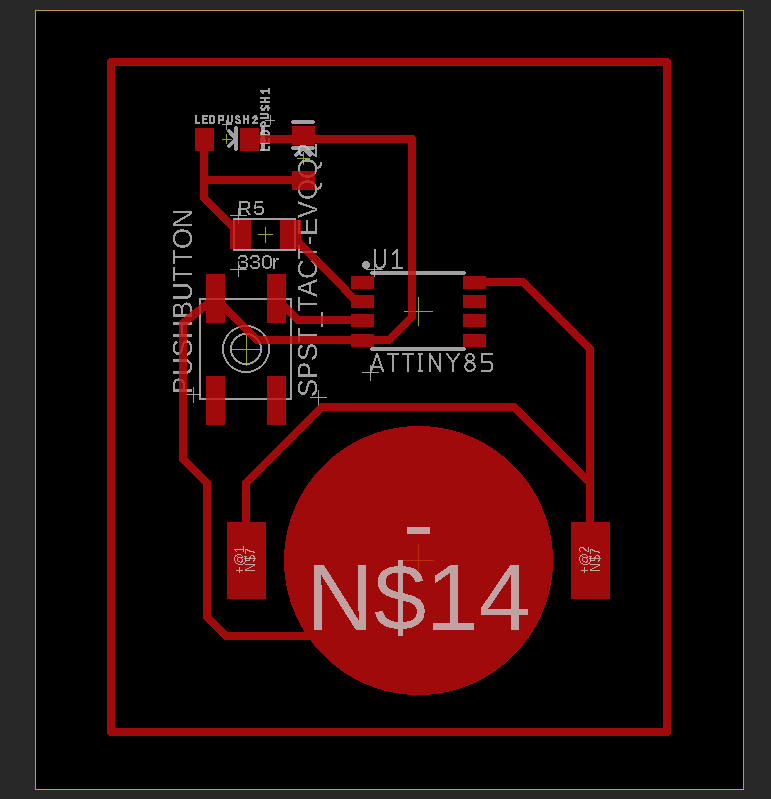 Board of the hello_world board
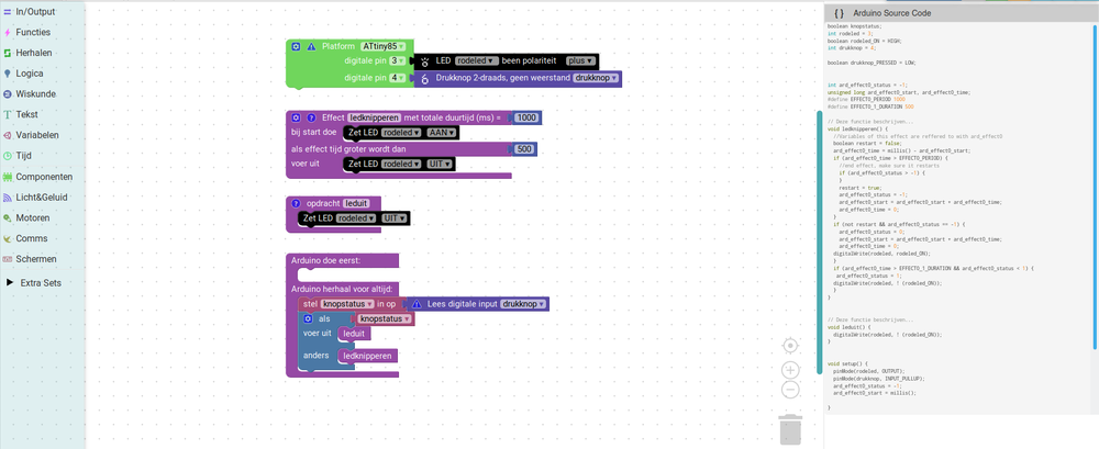 Code in Blockly for the hello_world with Arduino code next to it.
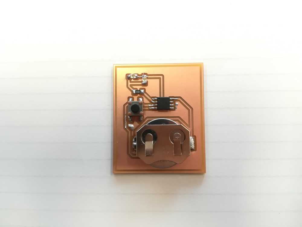 Hero shot!
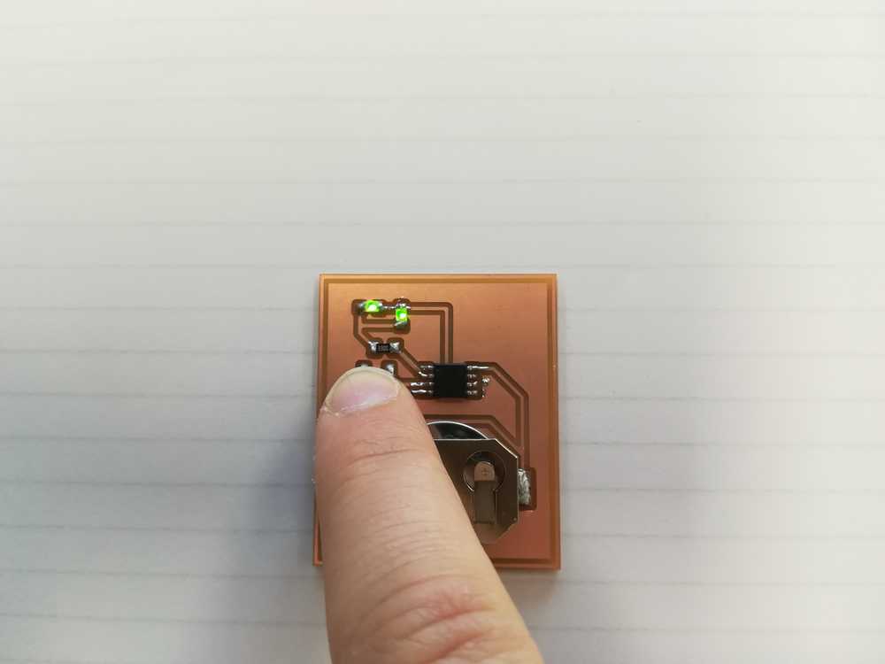 Hero shot!
 Hero shot!
To top
Reflection on this week
Feedback on this week: no one can ever prepare you for diving into a library. It's overwhelming! And you need to learn a lot. Next to that, making pcb's without any knowledge of electronics is hell, even if it's just the hello world board. Taking a coin cell battery and making a LED lit up is easy, but once you start with the micro controllers you need to keep in mind all the information from the data sheets. This ain't just a walk in the park.
But there is also good news. This time I did have a backup system to ask questions to. This time I did learn a lot about the whole electronics design and found my way around in Eagle. I also realized that I'm to impatient to learn new things. Curious but impatient. I noticed it a lot when watching video's on how to work with Eagle and my questions running ahead all the time It's frustrating and annoying. But apart from the schematics and libraries, I do like to play around in Eagle and designing boards. And the production of it is even more fun. So yeey, I made progress.
Another point is time management. It took me 3 weeks (with breaks) only to draw and etch the board. I did a big deal of learning, but it's to slow to keep up with the academy. For now I still have some relaxed weeks ahead (molding and casting, Make something big) but after that, play time will be over and I'll need to change my strategy on drawing and making boards.
Summary for this week:
