Task 5
Electronics production
In this week, I was given a task to have a group assignment and an individual assignment. The group assignment was to characterize the design rules for your PCB production process and the Individual assignment was to make an in-circuit programmer by milling the PCB, program it, then optionally try other PCB processes
PCB Fabrication
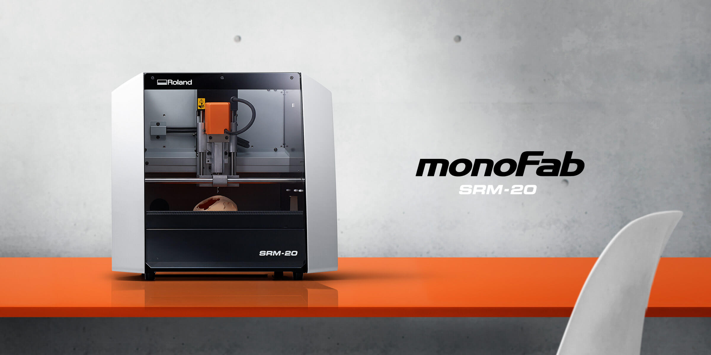
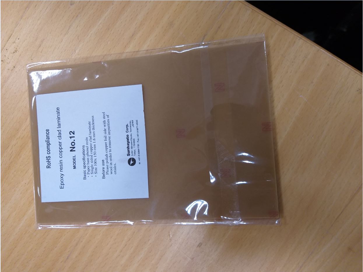
For the PCB Fabrication, we use milling machine Roland SRM-20 which is in our Fab LAB. We will use FR-1 (phenolic paper) PCB which has light sensitive coating for this assignment.
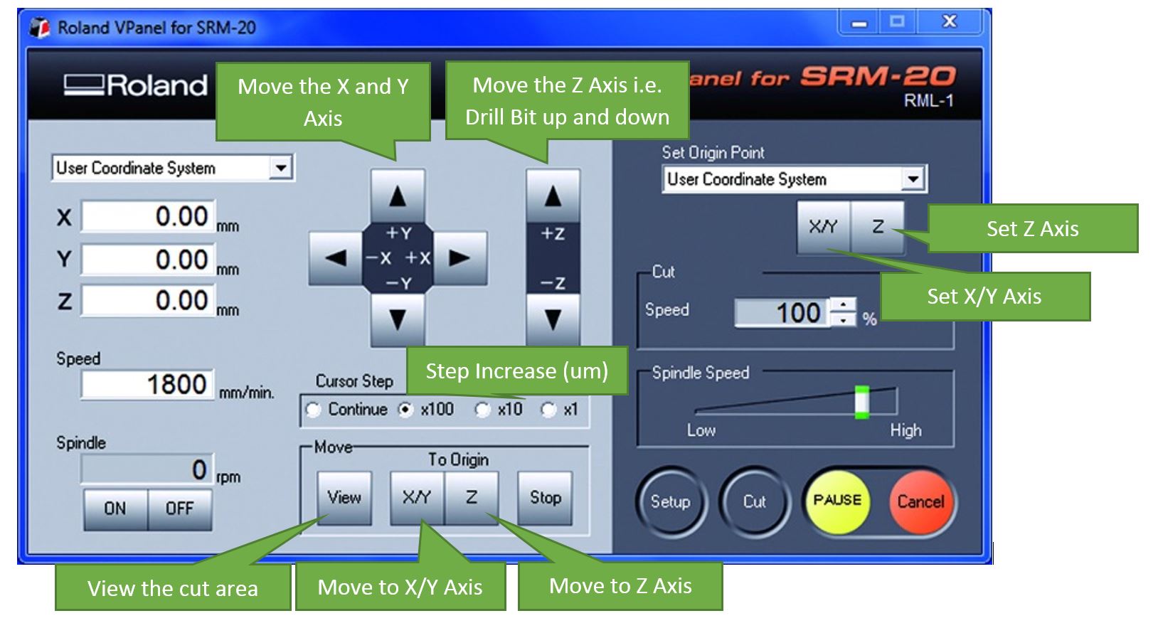
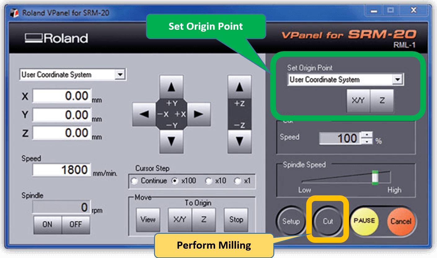
Roland SRM-20 User Interface Panel, inorder to understand how the User Interface works.
Creating .rml Files
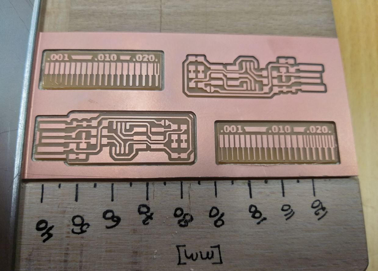
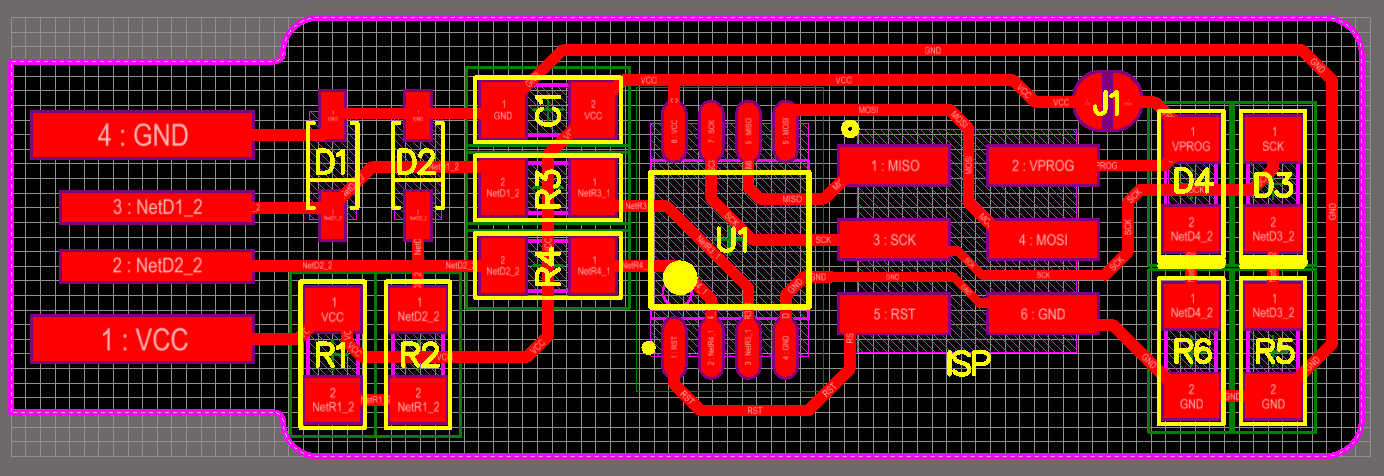
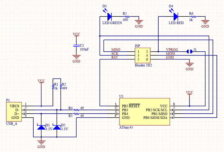
For the files creation, I selected my AVR ISP programmer card as Brian's work.
- I downloaded the ready made PNG files for the traces and the board outline from Brian's page.
- Outline Cutout (1000 dpi)
- Traces (1000 dpi)
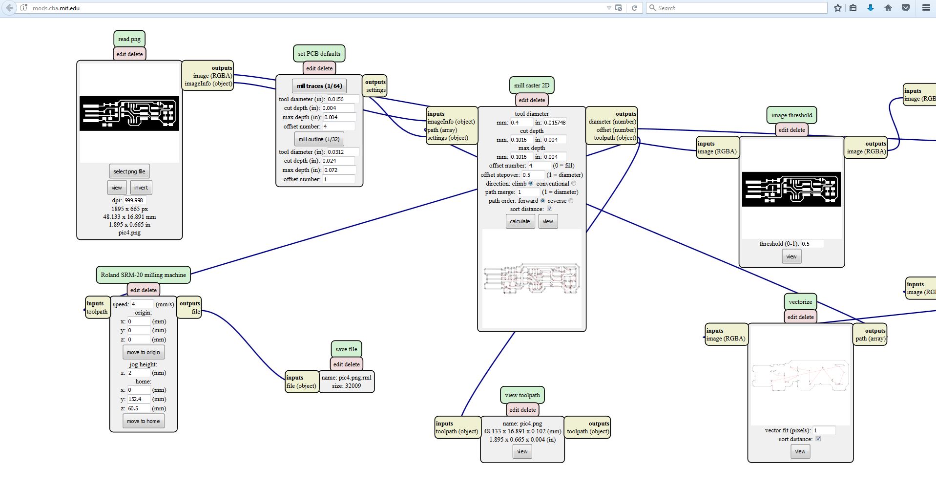
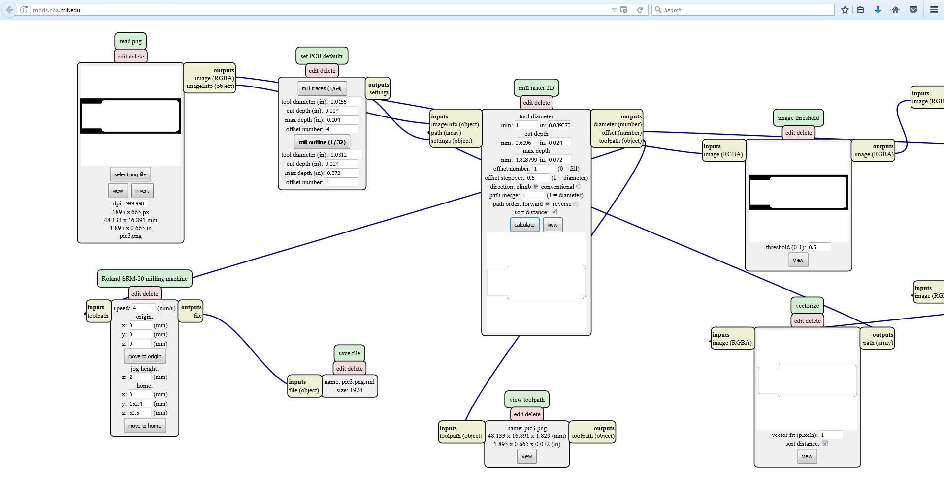
I selected Brian's Traces (1000 dpi) .png file and Outline Cutout (1000 dpi) .png file as an input, .rml (Roland mill) as an output and PCB outline (1/32) AND PCB traces (1/64) as a process. To create the rml files, I used mods. Below are the .png files.

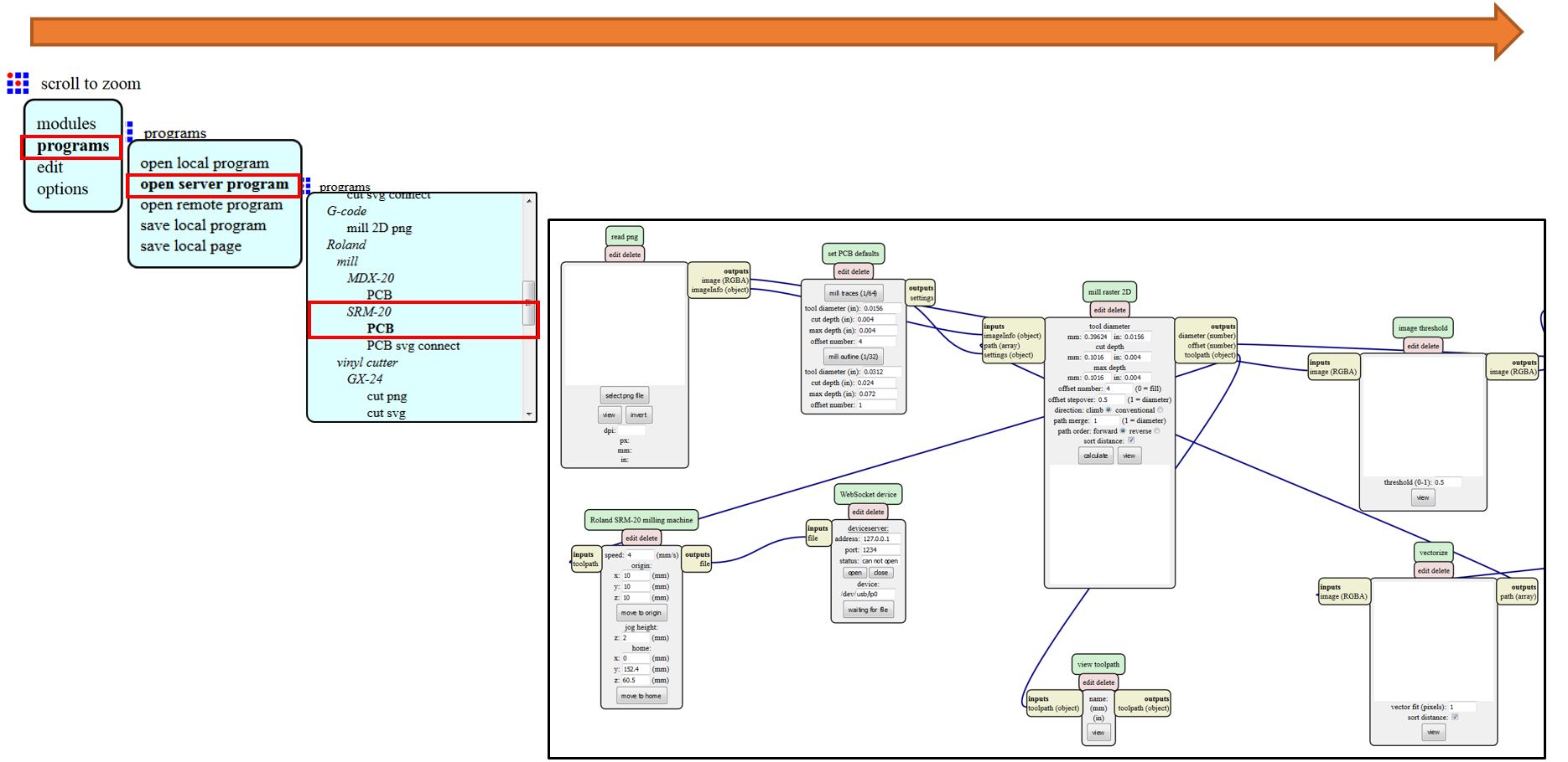
- Below steps need to be followed to get starter with mods.
- Open mods, As shown below Goto --> Menu --> Programs --> Open Server Program --> SRM-20 PCB.
Traces Creation (.RML Files)
- Below steps need to be followed to create traces.
- In the top left read png block select the .png file.
- In the PCB default block, select the mil traces (1/64).
- In the mil raster 2D block, select the mil bit size(tool diameter) i.e in mm you are willing to use. In my case I used 0.4mm for this process
- In the Roland SRM-20 milling machine block, select the origin x, y and z which is in mm to 0.
- To save, First delete the websocket device block and load the save block. To Load, Right Click select modules--> open server modules-->save
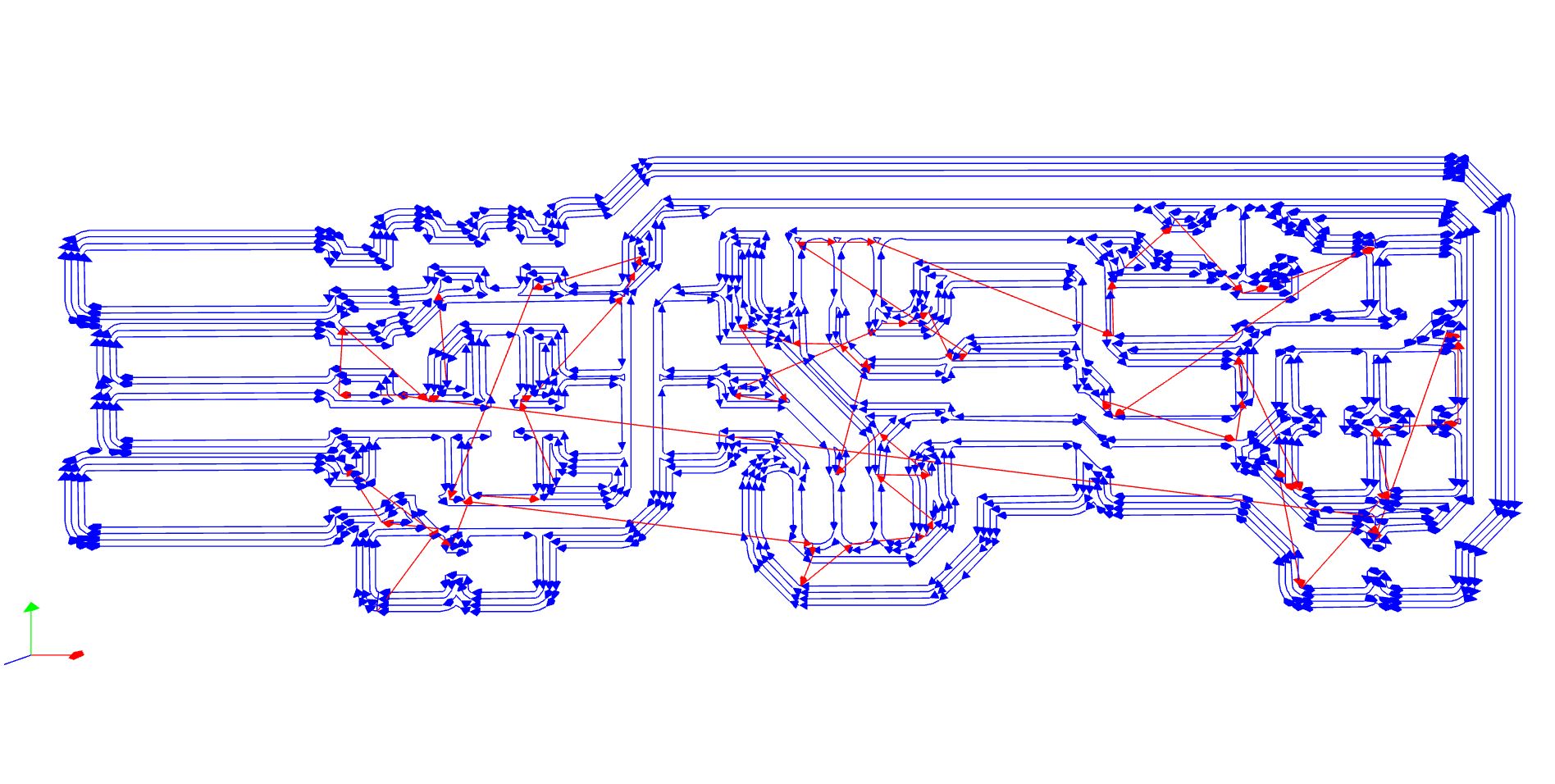
- Finally, mil raster 2D block, calculate and our design will be calculated accordingly and saved.
Outline creation (.RML Files)
- Below steps need to be followed to create traces.
- In the top left read png block select the .png file.
- In the PCB default block, select the mil outline (1/32).
- In the mil raster 2D block, select the mil bit size (tool diameter) i.e in mm you are willing to use. In my case I used 1mm for this process
- In the Roland SRM-20 milling machine block, select the origin x, y and z which is in mm to 0.
- To save, First delete the websocket device block and load the save block. To Load, Right Click select modules--> open server modules-->save
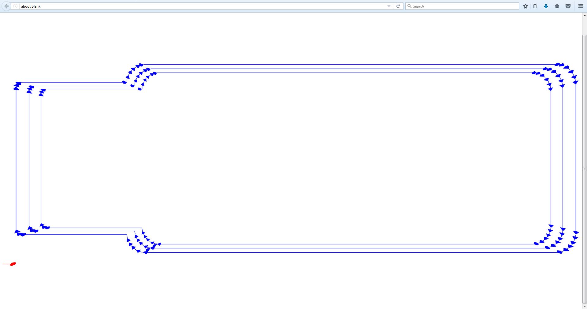
- Finally, mil raster 2D block, calculate and our design will be calculated accordingly and saved.
Milling the PCB
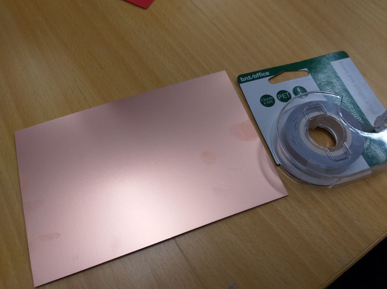
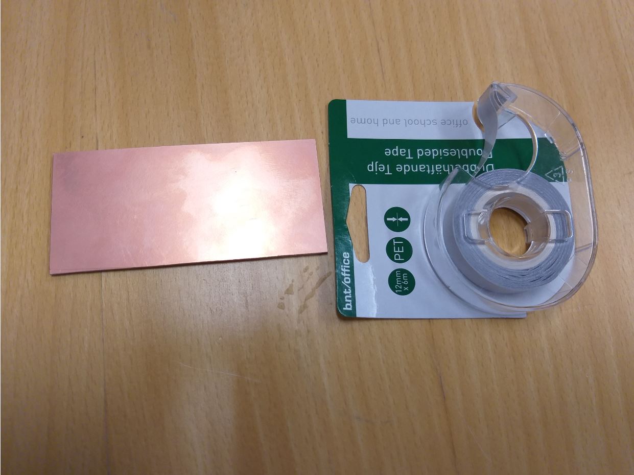
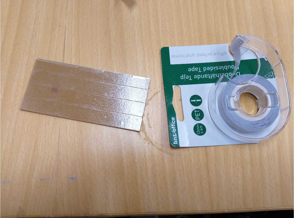
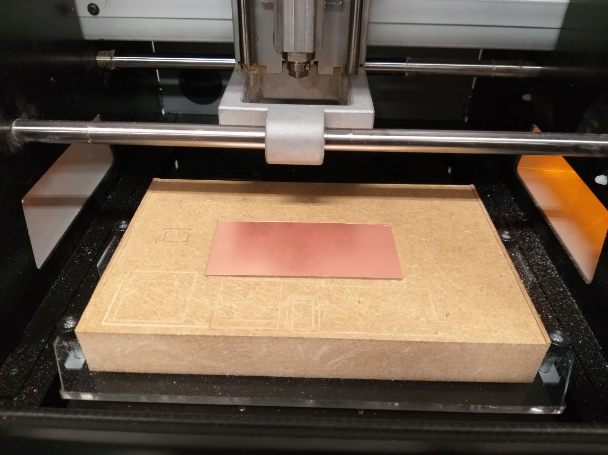
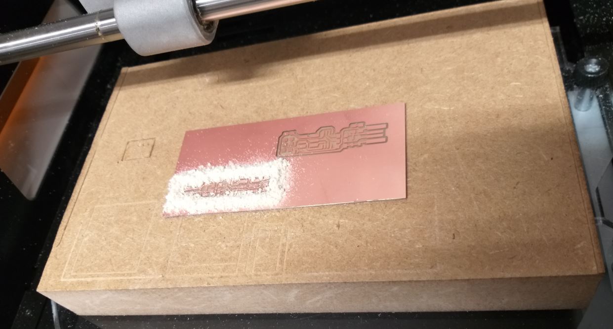
First, I took a new FR-1 PCB and then I fixed the position of the PCB board on the wooden board with double-sided tape. Copper layer of circuit board is about 0.03mm, so it is important to keep the board flat when we manufacture PCB. Since the PCB that I was using was big enough thereby I cut it down and then double taped it. I carefully applied the double-sided tape without overlapping each other.
I cut down the PCB as per my requirement, as said earlier it is important for the board to be as flat as possible and it makes sense the smaller the board the more flat it is.
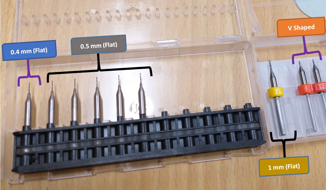
- These were the milling bits available in FAB Lab:
- Traces : 0.4 mm.
- Traces : 0.5 mm.
- Traces : V shaped.
- Outline : 1 mm.
- Outline : 0.8 mm.
The used 1 mm for Outline and 0.4 mm for traces. The traces bit was selected due to its least diamater i.e 0.4 mm and high precision.
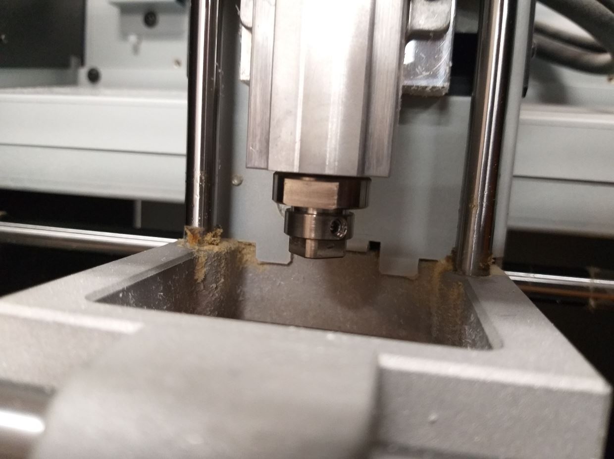
- Choosing the required Mill Bit, and setting up the origin is extemely important before starting to milll the PCB.
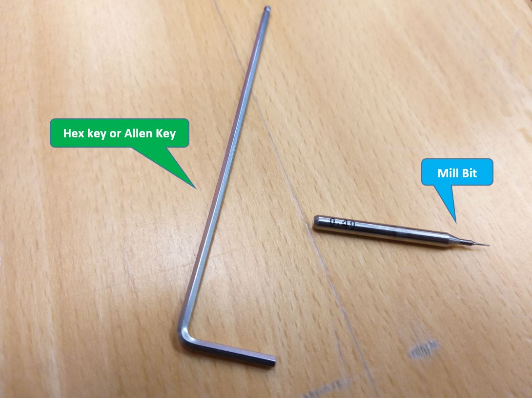
- Mill Bit Setting : using the required mill bit and the hex key or allen key to tighten it
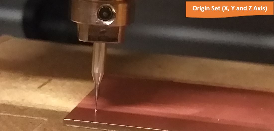
- Setting Origin : using Roland V Panel for SRM-20, Move the head to in the left of right position (The Starting point where we are willing to start the mill). The Left and right buttons will assit in that regard, press X/Y to set origin (X and Y Axis Coordinates) button and Z to set the Z coordinates. Z-axis settings is important to consider and require a precision work to avoid any bit damage during movement. The step increase for z-axis have to be small as possible and the z-axis is adjusted in such a way that a gap of just a few millimeter/micrometers between the PCB material and the mill bit shall be left. Then, the Hex key/Allen Key as seen in the picture below shall be utilized to loosen the mil bit and ease it to the PCB surface, after that tighten it again. Set the Origin Point for the corresponding axis i.e. Z Axis. Therefore, the origin i.e X,Y and Z-axis are set now.
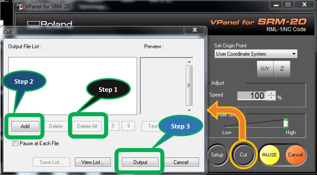
After having the required settings of the Origin, to perform the milling press cut -button, which opens the window, delete all -> select file, and after that pressing output, the milling process will begin as seen in the picture.
Group Task
- The group assignment was to characterize the design rules for your PCB production process. I downloaded the files from Fab Academy Electronics Production Page for Linetest Traces and Linetest Outline. For this process I used:
- Case 1 : Traces 0.4 mm (Flat) and Outline 1 mm.
- Case 2 : Traces 0.5 mm (Flat) and Outline 1 mm.
- 1x ATtiny45 or ATtiny85
- 2x 1kΩ resistors
- 2x 499Ω resistors
- 2x 49Ω resistors
- 2x 3.3v zener diodes
- 1x red LED
- 1x green LED
- 1x 100nF capacitor
- 1x 100nF capacitor
- Put a bit of solder in the pad of one of the sides/legs to hold the component
- Then position the component over it and heat the solder with the iron tip so it melts enough to hold the component
- Likewise, proceed to solder the other side/legs of the component
- Atmel GNU Toolchain
- Gnu Make
- avrdude, Installation not needed, just run it
- C:\Program Files\avr8-gnu-toolchain\bin
- C:\Program Files (x86)\GnuWin32\bin
- C:\Program Files\avrdude
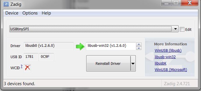
- Download Zadig and launch it
- Plug in your programmer, and select the "USBtinySPI" device in the list
- Select the driver: either libusb-win32 or libusb0 and Install the Driver.
- Get fts_firmware_bdm_v1.zip from Brian's and unzipped it
- Open GIT Bash Inside the firmware unzipped directory
- First check the :


As explained earlier for the settings, I used mods to make the rml files from these png files.
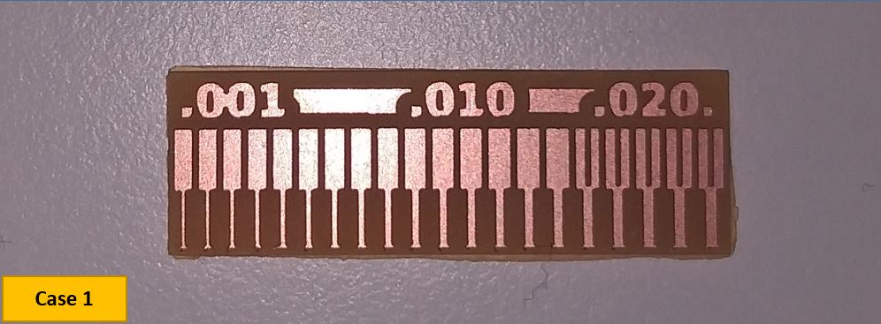
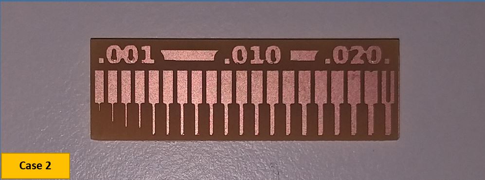
Case 1: Milled with 0.4mm and Case 2: Milled with 0.5mm, it can be observed that using the 0.4mm mill bit it is possible to mill the pcb that require precise and smaller details than using the 0.5mm mill bit. It is found that the smallest dill diameter of 0.4 is able to drill 0.001 mm thicker lines. Hence it is summaries that smaller the drill diameter good for file line milling.
Individual Task
PCB Milling
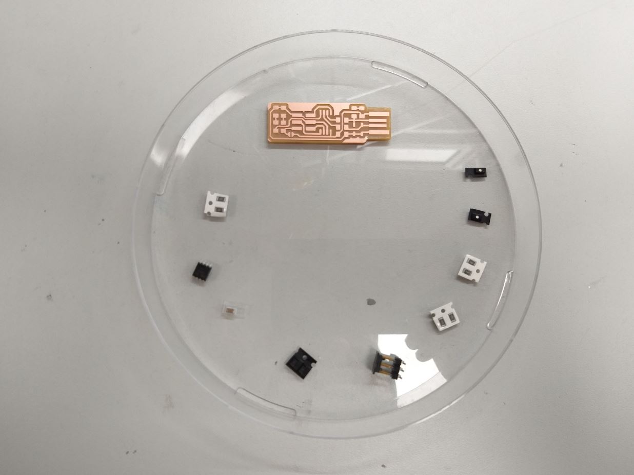
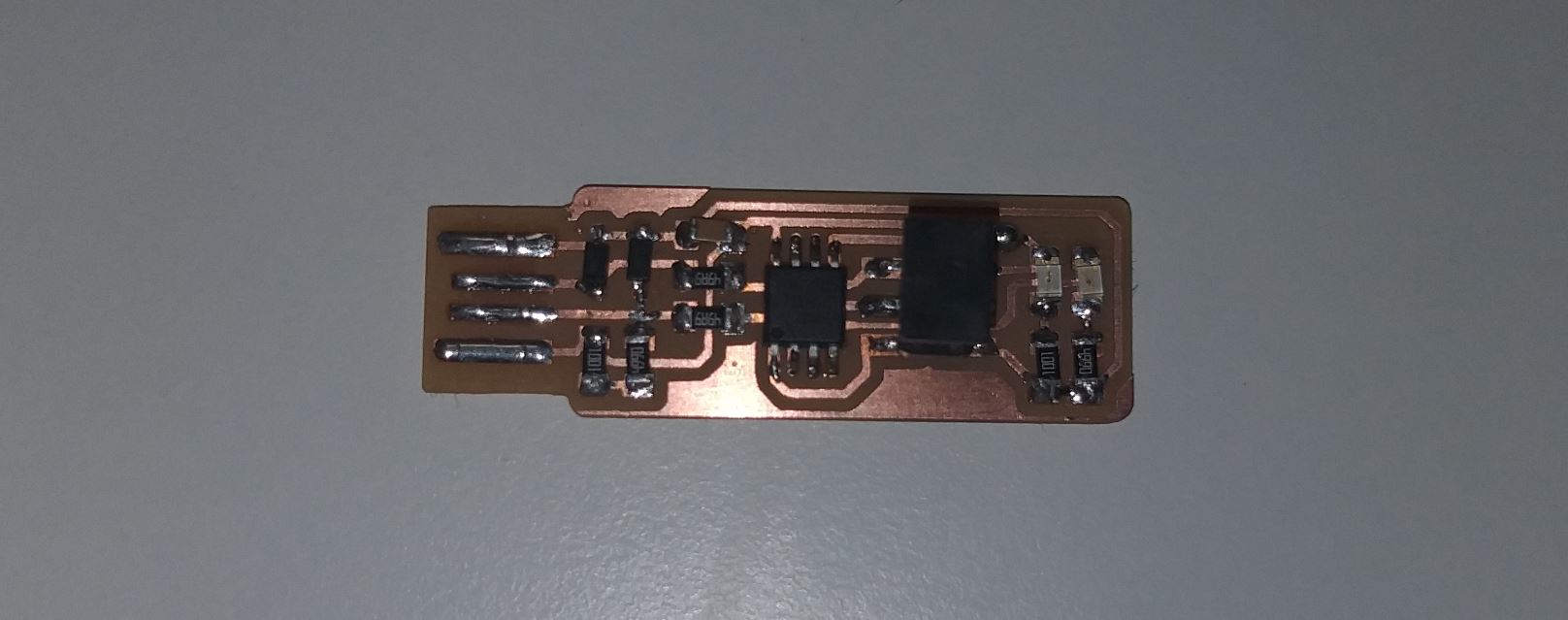
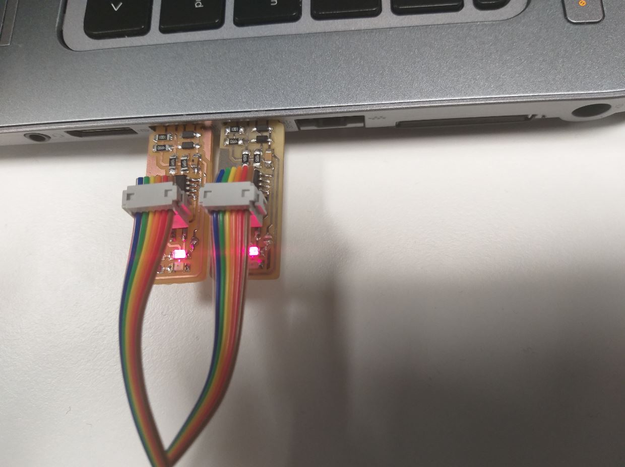
The PCB Milling for my Individual Task to mill the Brian’s isp programmer board is being done with the same methodolody as explained earlier. In the picture below, the milled board can be seen
Soldering Components
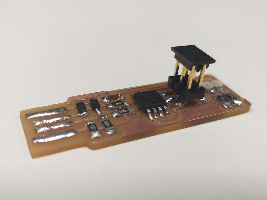
I have previously used soldering iron for through-hole components. I have also soldered surface mounted components using soldering paste and a reflow oven. However, it was the the first time I used the soldering iron to solder surface mounted components. After a few attempts I felt "brave" enough to try to solder in the real board.
- I collected all components, The necessary components according to Brian's instructions are:
The board image and the schematic is obtained from Brian's webpage:
- Solder Steps to follow:
Programming
- I followed again, Brian's page. I am a user of Windows OS, therefore, I had to install:
Path Updation for avrude: Control panel --> System --> Advanced System Settings --> Advanced --> Environment Variables button --> User varianles --> Path --> Edit
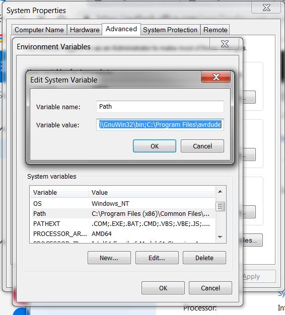
- Three Paths to be added:
- Next step is to install drivers for the Programmer:
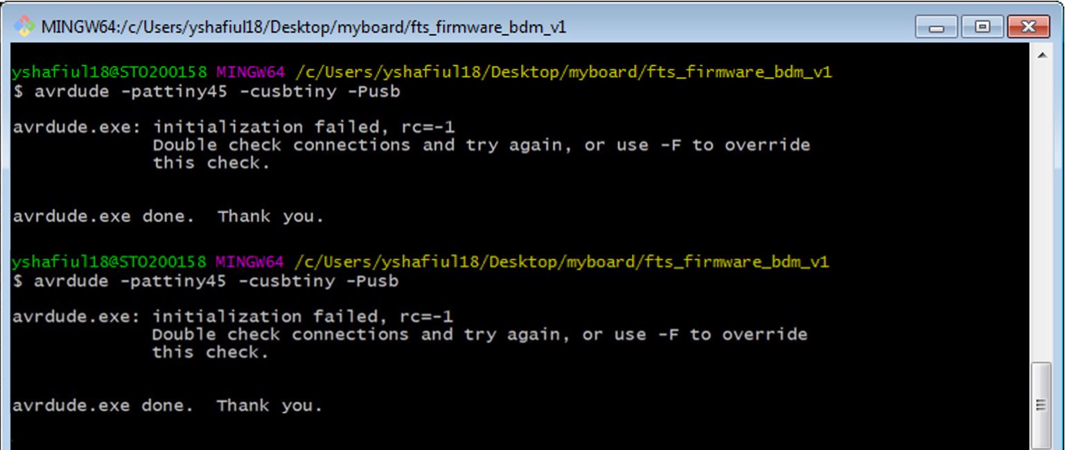
I downloaded the HEX code files (fts_firmware_bdm_v1.zip) from Brians Page and ran a series of commands which are mentioned below.
- Installation Check :
‘make -v’avr-gcc --version avrdude -c usbtiny -p t45
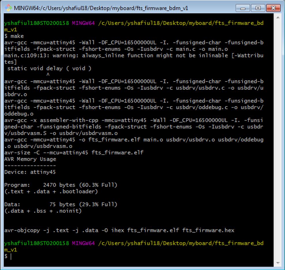
- Get and Build the Firmware :
- Run
make [To create the hex file]
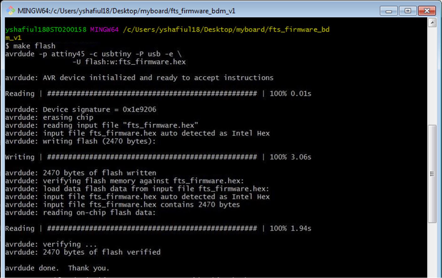
- Program the ATtiny45 :
- I plug my board into a USB and Connect the programmer which I got from Jari to the ISP header on my board
- Run
make flash [program the .hex file]
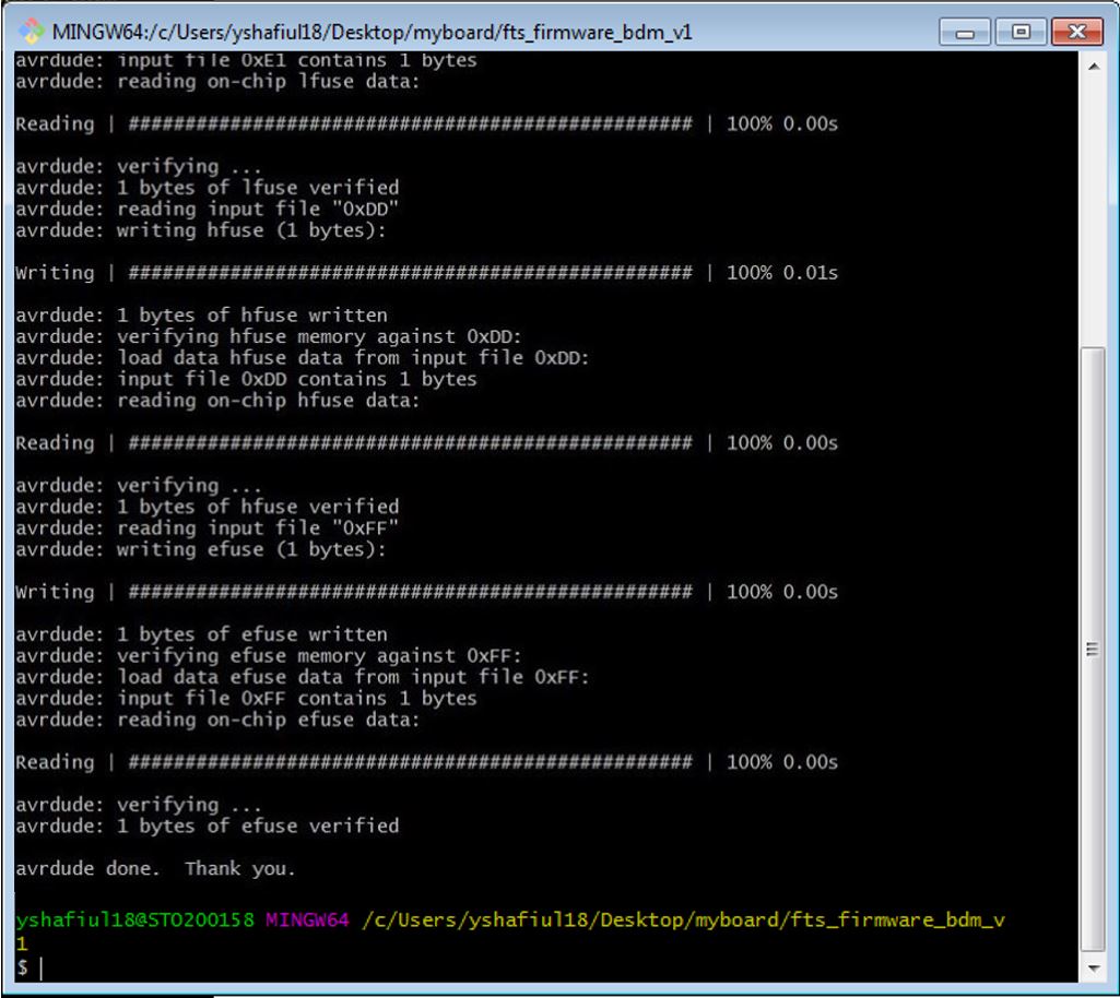
make fuses [Set the fuses so the board will use the external crystal]
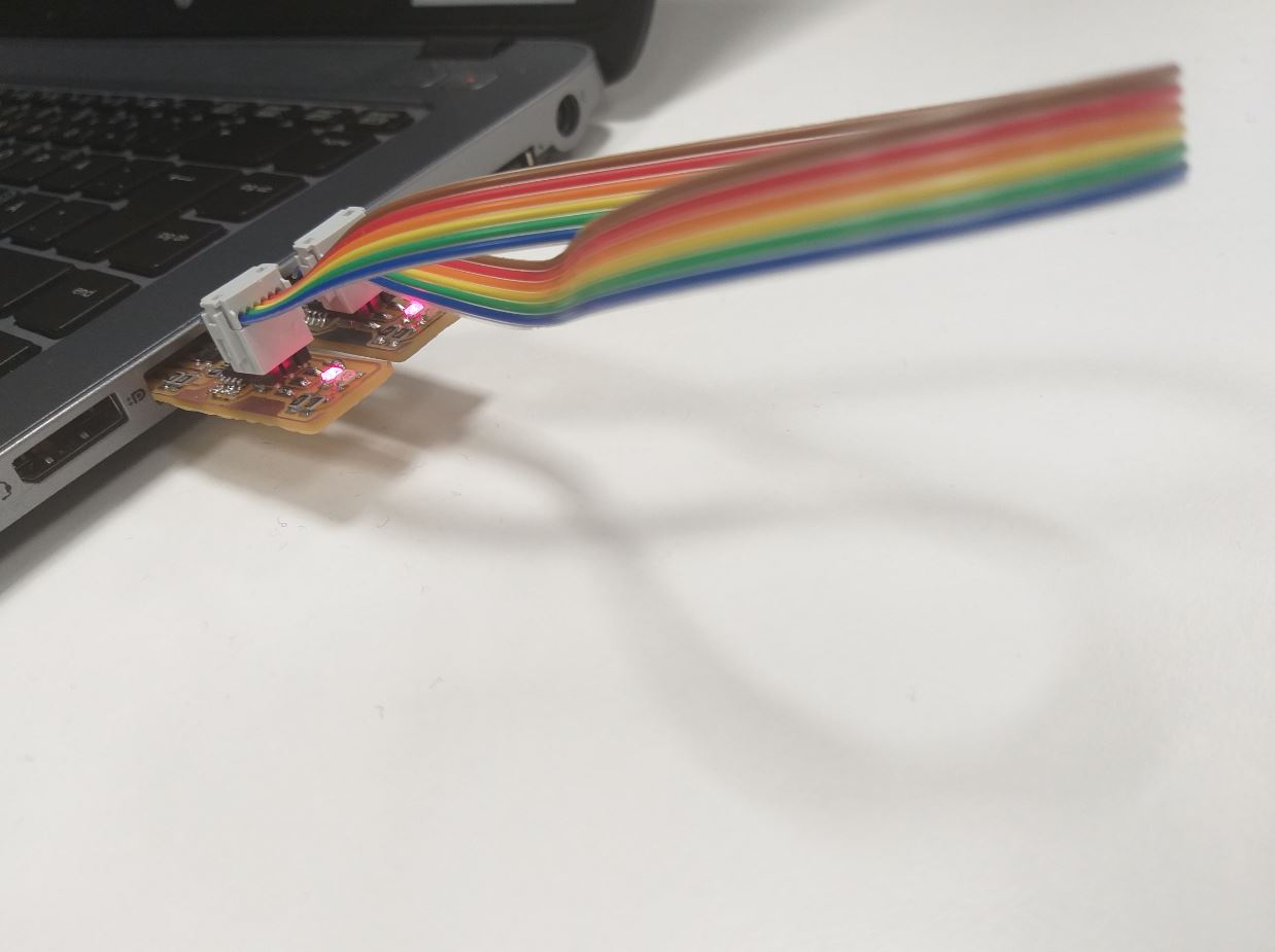
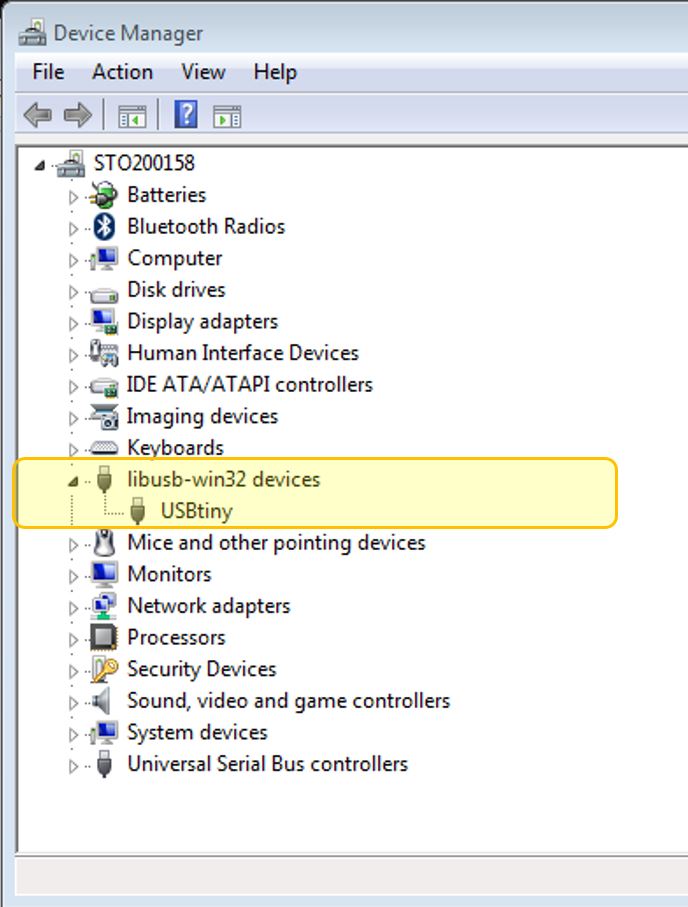
- USB Functionality Test :
- In Windows Manager, you will be able to see your programmed device in the device manager
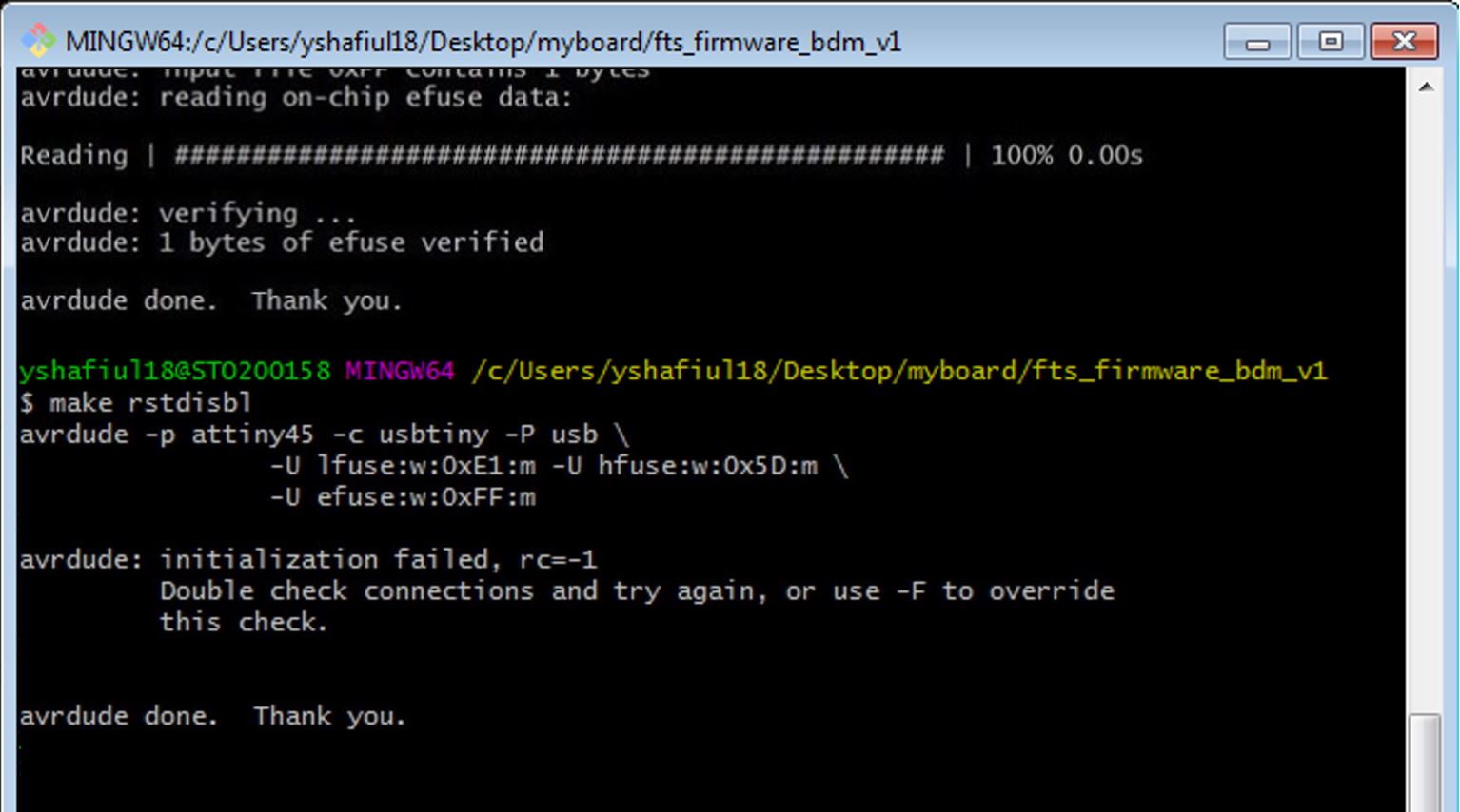
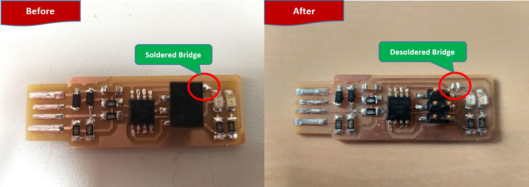
- Making the USB non-programmable:
- In the GIT Bash, type
make rstdisbl [This will make the usbtiny non-programmable]
Resources Utilized
- I utilized these resources for this task:
- Atmel GNU Toolchain
- Gnu Make
- avrdude
- Zadig
- git
Files
- Group Task : Trace PNG File
- Group Task : Outline PNG File
- Group Task : Trace RML File (0.4mm)
- Group Task : Trace RML File (0.5mm)
- Group Task : Outline RML File (1 mm)
- Individual Task : Trace PNG File
- Individual Task: Outline PNG File
- Individual Task : Trace RML File
- Individual Task : Outline RML File
- fts_firmware_bdm_v1.zip
- Created: (fts_firmware.hex)