_week 7
electronics design
Group assignment
For this weeks assignment we have to redraw the echo hello-world board (which is a microcontroller) adding two new components one LED(with its resistor) and one BUTTON (with a pull up resistor).
During the group assignment we learned how to use the Oscilloscope helped by a former
student of the FabAcademy Sreejith Mohanan.
We used it to test one of ours MCU boards to see the signals our resonator was emitting.
But first.....
_WHAT IS AN OSCILLOSCOPE?

An oscilloscope is an electronic device that serves to test and analyze varying signal voltages.
These signals are represented graphically on the oscilloscope, and you can read the signals of one, two
or three different inputs and compare them graphically.
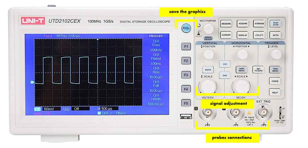
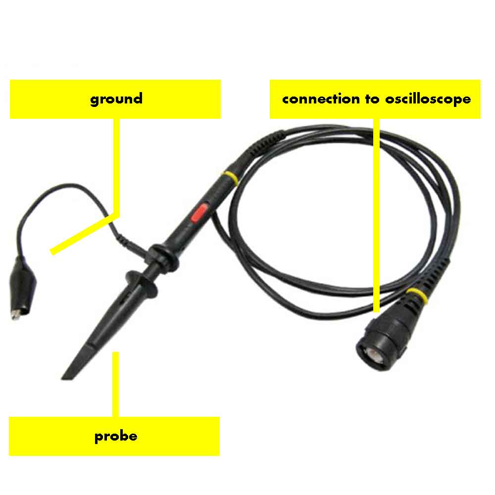
The oscilloscope uses "probes" that serve to track the signals on your circuit.
The probes have a clip or hook to touch the circuit component, and it has another probe attached that
serves to locate GROUND on the board you are testing.
The "alligator" type probe is the one that goes into GROUND.
Here's a short video we did trying to read the signals the resonator was emitting.
If you are interested, here's a useful tutorial that goes deeper on how to use an oscilloscope.
SPARKFUN OSCILLOSCOPE TUTORIAL
There is another device that we've been using and is essential when you are doing circuit board to tests the connections or possible short-circuits.
_MULTIMETER, WHAT IS IT?
The multimeter is an electronic device that measures different functions such as; voltage, current and resistance in one same unit.
Just as the oscilloscope, the multimeter needs probes to test the unit, they are called leads.
These probes can be connected into three slots: "COMMON GROUND COM"(normally the black lead), "Ammeter
terminal" and everything else but ammeter terminal (ammeter measures the electric current).
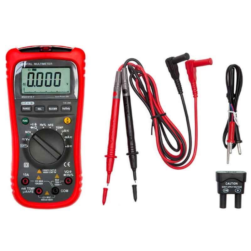
_CONTINUITY TEST
One of the commom and useful thing you want to do when building a circuit is to check the
CONTINUITY of your components.
The continuity test serves to check the presence of a current flow between points.
To test it set the multimeter to "continuity" (looks like a flipped icon)
Test the probes by touching them together, they should emmit a bip!
Using the probes touch different separate pins. If you hear a tone it means they are connected.
Here you can find two useful tutorials that give a more in-depth description of how to use the multimeter for other tests SPARKFUN MULTIMETER TUTORIAL, and FLUKE MULTIMETER TUTORIAL
Individual assignment
So here I am unfamiliar to this new world of electronics (although I did already a FABISP, but still this is a hole new language for me), attempting to design, fabricate and test my first microcontroller all from scratch...
Before getting my hands on working on the microcontroller here is some information about what I will be working with.
1_redraw the echo hello-world board
2_add (at least) a button and LED (with current-limiting
resistor)
3_check the design rules, make it, and test it
Before I explain each tasks, let's start understanding what is a microcontroller?
A microcontroller or MCU (microcontroller unit) is like having a small computer built on one
integrated circuit.
Microcontrollers are used in automobile engine control systems, implantable medical devices, remote
controls, office machines, appliances, power tools, toys and other embedded systems (a controller, I
am still unfamiliar to what an embedded system does, but we will cover it up the following weeks).
_List of materials
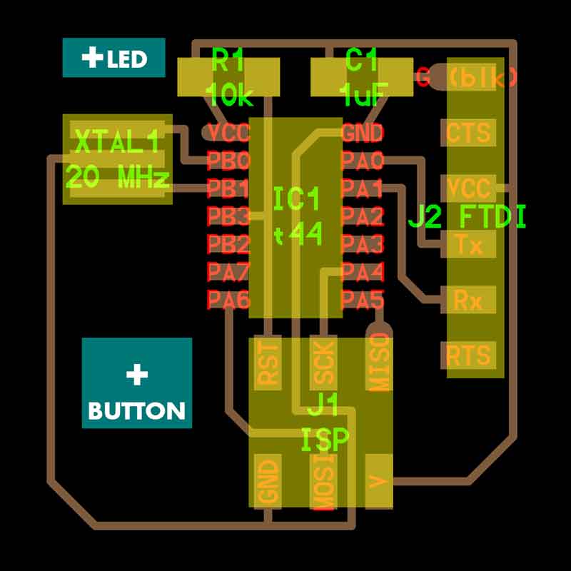
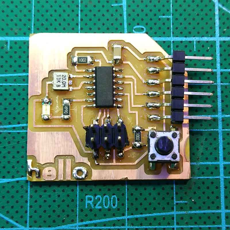
MCU are designed using different components, for this take we followed the example from the echo hello-world board adding a few more components. Below is an image of the board we will be using as reference, and in an effort to understand and learn better, I will try to explain in my own words what each component does, because there must be a reason why they will be welded on our board, right?
Ok, so what do we have here... we will be using:
1_ATtiny44, it is our microcontroller, it is like the
brain of the circuit. It is a programmable component that we will program afterwards from the computer.
On the diagram it appears with the tag of IC1t44
The ATtiny44 we are using has 14 legs, each of them has a function and it is crucial to understand which
one has to be connected to what component, so it is handy to have the datasheet of the ATtiny44 so you
don't forget which leg goes where.
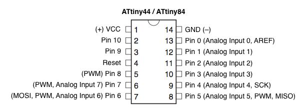
Important tags to remember and their meaning
VCC (voltage at the common collector) it is where circuits get their
voltage. In our case the
voltage comes from another device and commonly the main power input is 5V.
GND (ground) as the name says is the base 0V level
SCK, serial clock to synchronize the data that is being "spoken" among the ISP and your new
microcontroller
MOSI is the output
MISO is the input
2_Resistor of 10k/10 Ohm, they are used to reduce the flow of the current, in this case we need it to keep steady the flow that goes into the microcontroller near VCC and for the RESET signal.
3_Capacitor 1uF, the capacitor storages voltage that is used to regulate the flow in the circuit in case there are any spikes of current in the voltage.
4_FTDI , this component is where we will connect a
special cable (FTDI cable) that serves to connect the microcontroller to a USB port and translate the
serial language from the MCU to USB language. Inside the FTDI cable USB port, there is an integrated
chip that emulates the serial language so that USB-serial language can communicate.
It's pins VCC and GND have to be connected to the VCC and GND on the board. TX and RX prins go to the
free pins on the MCU.
TX : transmit RX: receive
5_SPI header pin(Serial Peripheral Interface), this
component will connect your MCU to your FABISP to take the data needed, so you will see that MOSI, MISO
and SCK (input and output pins) connect to your MCU. You will notice that it has to be connected also to
GND and VCC.
SPI basically serves for communication between MCU and other peripheral devices.
6_Crystal Or resonator(XTAL), this component is an
external clock and it emits a signal at certain frequency (hertz).
MCU have a built in clock but external resonators are used to have a more accurate clock. This frequency
will tell the MCU how fast/slow to execute a task.
It is connected to theh free pins on the MCU PB0 and PB1, and needs to be connected to GND.
That is the list of components the echo hello-world board needs, however we will be adding two extra components, to why not make this task a bit more complex and fuse my brain a bit more:
+7_LED+10 Ohm resistor, you may know it's a light, but
LEDs belong to the diode's family, one of their characteristics is that they let go the energy in only
one direction.
Together with the LED we will need a RESISTOR as well. This is because the LED will emit light when the
current is passing, and the resistor helps to limit this current otherwise the LED would just burn,
unless the voltage is the same as the LED voltage drop.
To choose the right resistor you will need to apply Ohm's law to figure out the resistor you will be
using.
V= I x R V= voltage I= current R= resistance
In my case the voltage we are using comes from my computer USB port so it's 5V.
The current of the LED depends on the model you have, you can check on the FabLab INVENTORY the model, and then you
can calculate the resistance.
Once I knew the LED model I was using I checked the forward current and forward voltage on through HERE.
For the calculations I did it came out I needed a 180ohm resistor, for an LED with 20mA of
forward current and 1.75V.
Another way to calculate it is on this useful online tool that calculates the resistor you will be needing, check out HERE the online calculator.
+8_BUTTON+resistor, in this case we will be using the
button or switch to turn on and off the LED.
Buttons need a "pull-up resistor", they basically help to ensure that a pin is in a high or low state (0
or 5).
_SET UP EAGLE SOFTWARE
Ok... so now that you know which components you will be needing comes the fun part of drawing the
board.
I will be using a software from Autodesk, specially designed for PCB design, it is called EAGLE and it has a free license for students.
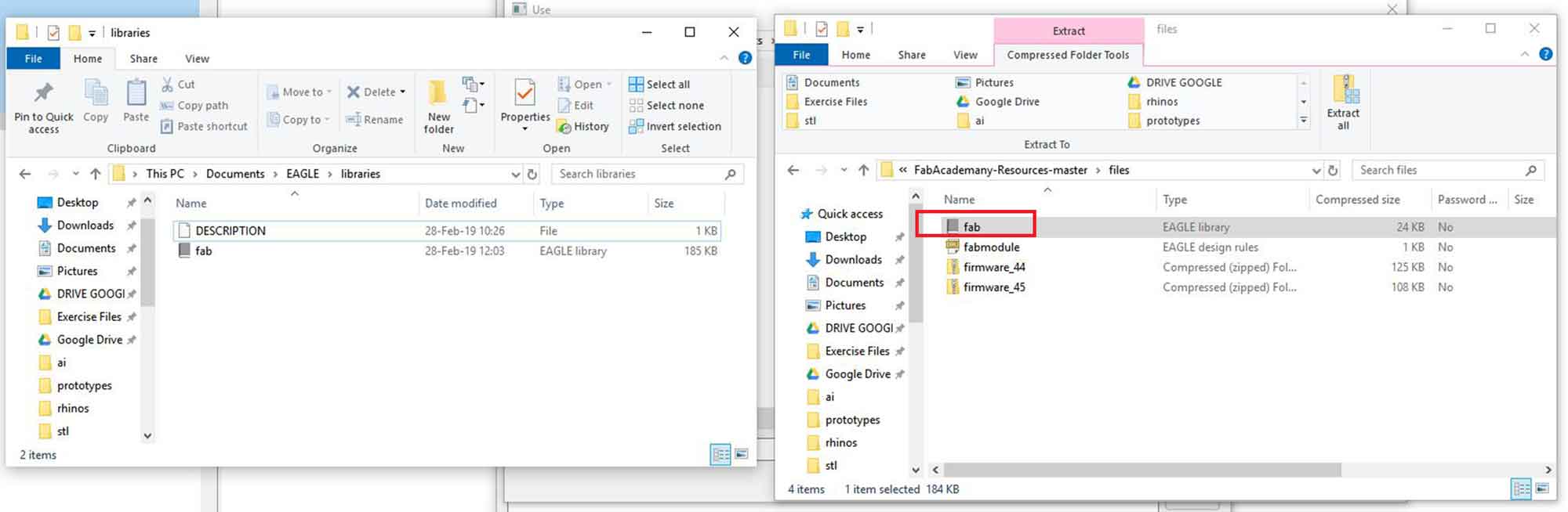
Eagle has a library of components included by default, in our case as we will be using materials that every FabLab has on their inventory, we will load a FabLab library into Eagle so we can work with them. You can download the zip from THIS link. You will be using the file called "fabmodule.dru" for the design rules and the file "fab.lbr" for the library of the components.
Extract the library into the folder of EAGLE where you have the installation, must likely (on Windows) is on DOCUMENTS>EAGLE> and go to libraries.
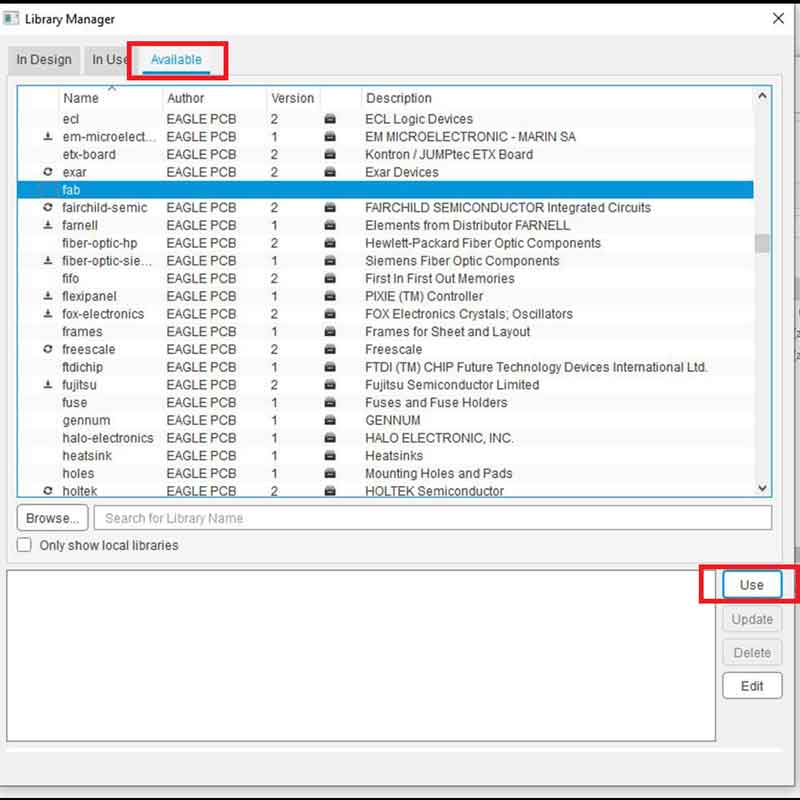
Then on EAGLE, go to Library>Open Library Manager, remove the ones that are inside "IN USE", it won't
delete them just remove from the available components in the library.
Then go to AVAILABLE and browse the FAB library and select USE, this will add it to your EAGLE library:
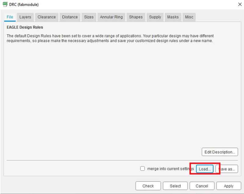
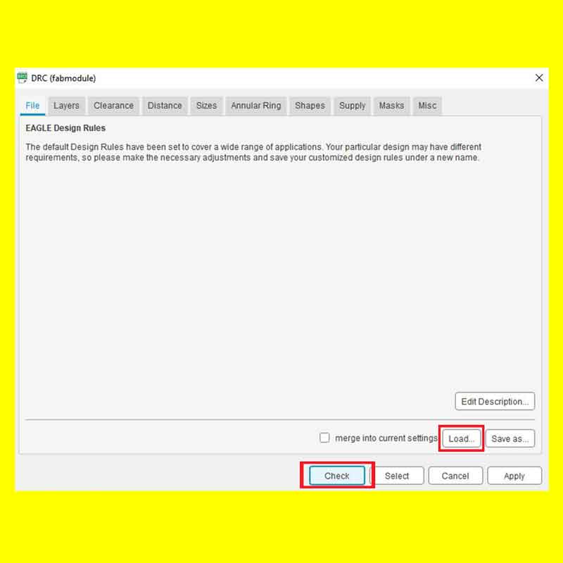
You need to load the DESIGN RULES as well, but what do Design Rules means?
DR are the settings of the your CNC machine which will limit the spcae between the traces and other
settings, so it is super important to load them before you start drawing the BOARD.
To do that just go to TOOLS>DRC and then load the file of the DESIGN RULES that is also available on the
previous link I wrote above.
_CREATING THE SCHEMATIC
After this set up you should be ready to begin drawing the SCHEMATIC of your board.
You need to begin by adding the components on your schematic, and this tools are the ones you will
using:
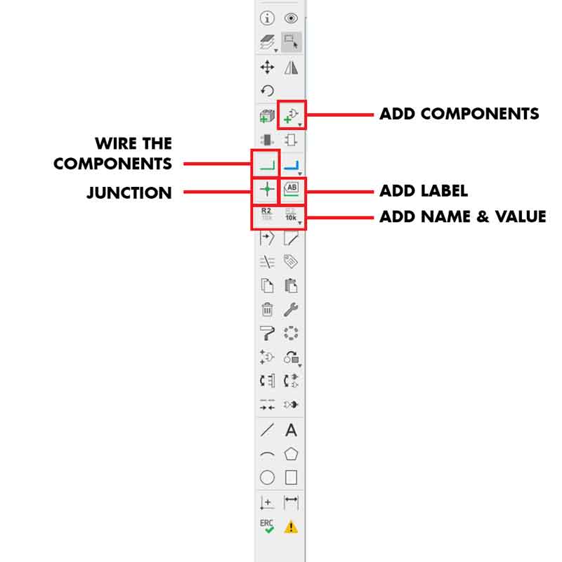
I suggest that you start by adding the components of the original ECHO HELLO BOARD and their
connections.
After that add the extra components.
This is how it looks when you select components from your library (make sure you are using SMD components from the FABlibrary).
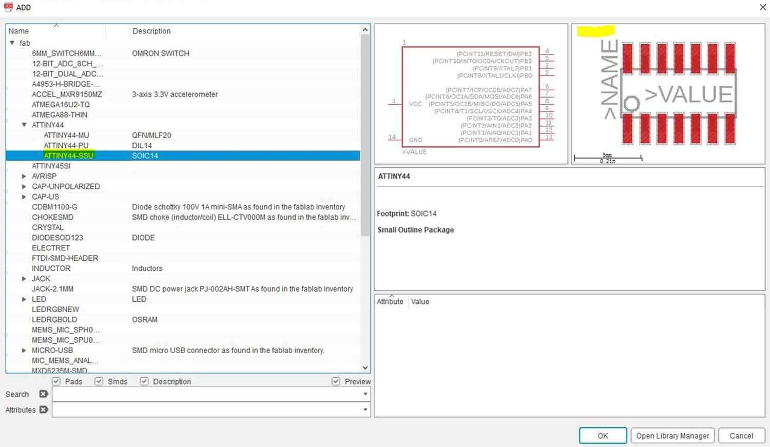
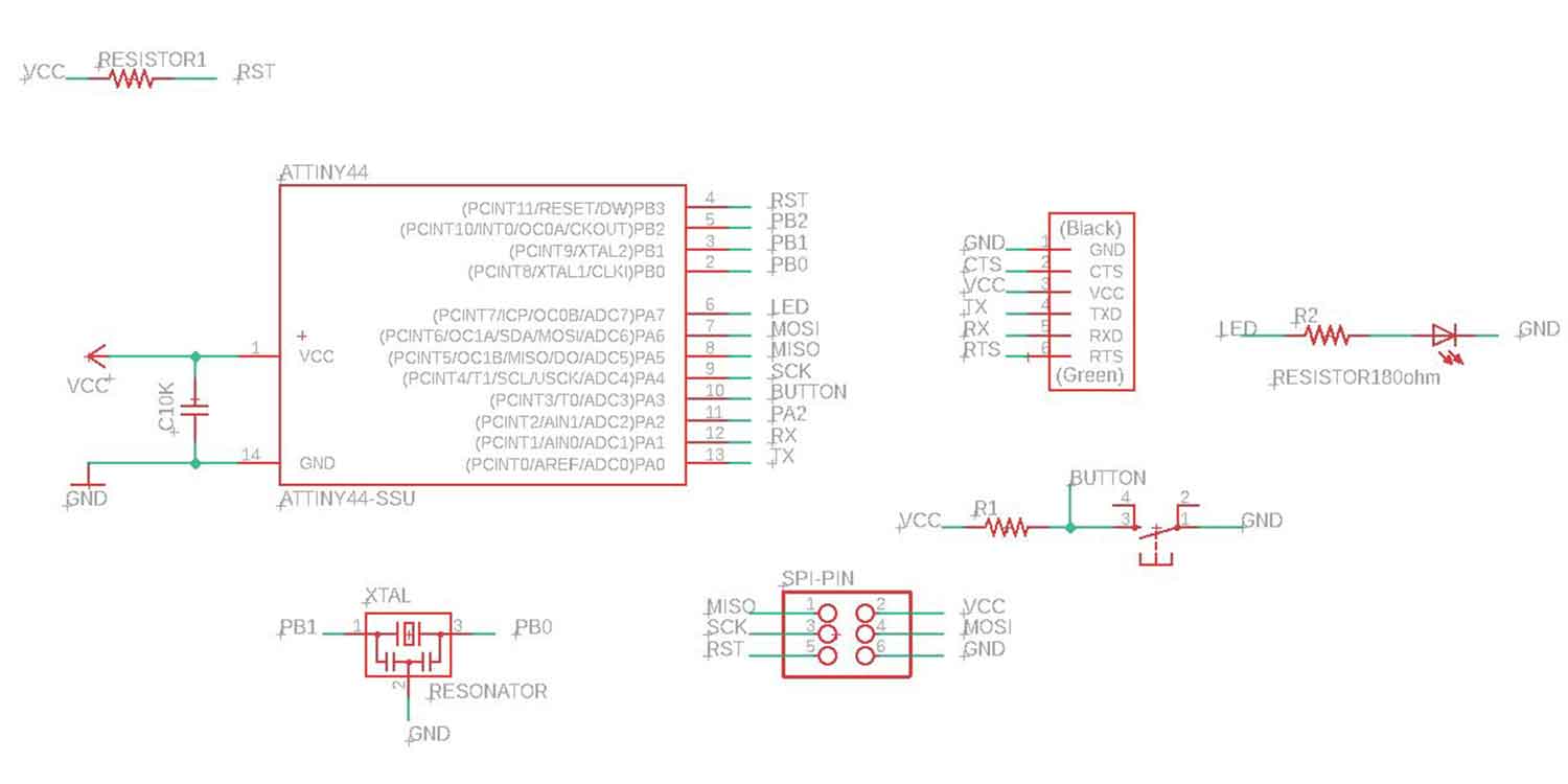
I first started by adding the ATtiny. Remember that this is not a real visualization of the physical
component, the schematic is only like a floor plan with the components and their connections, it doesn't
matter if you place one component closer to another, the important thing are the connections.
This is how it looks in the schematic:
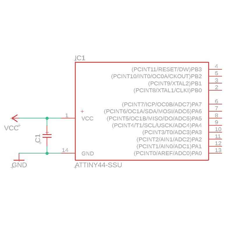
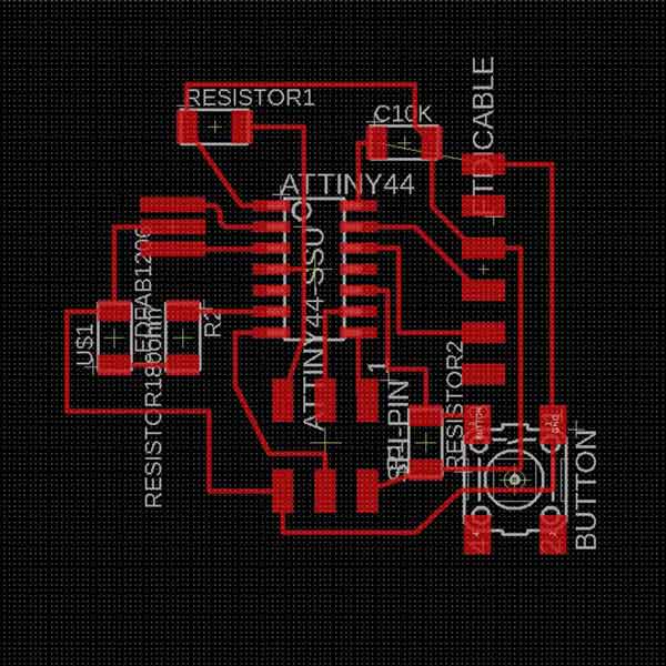
This is my final schematic with all the components and their connections:
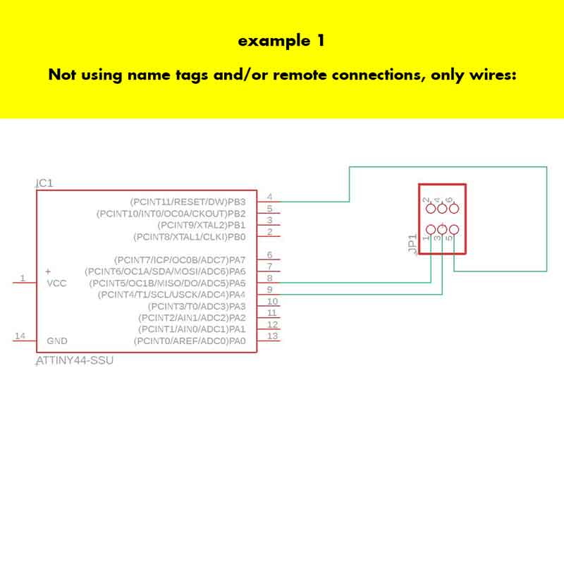
In the schematic is quite useful if you add labels to name each extension in the components, this is
visually very useful otherwise you will end up having lots of wires around your schematic.
Here I drew two exampled of how visually you can connect your components on EAGle.
You will notice how clean and easy to read the connections is example 2:
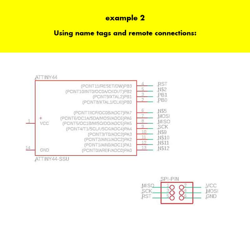
On the following video I show how to do this shortcuts and add tag names to the components:
This is how my final schematic looks like:
_GENERATE BOARD
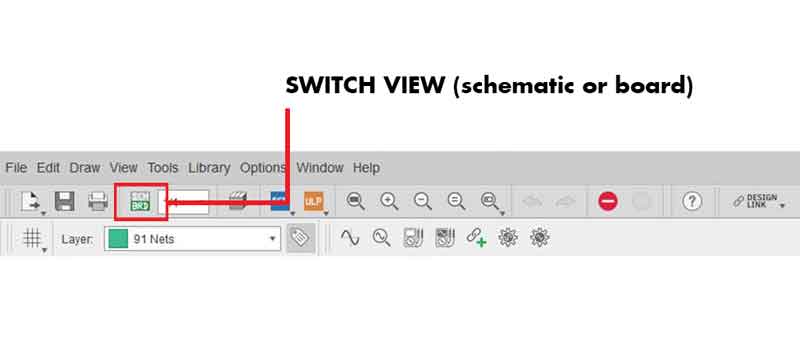
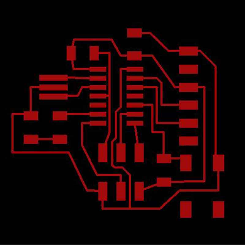
Once you have finished adding and connecting your components on the schematic view, you have to switch to BOARD view you have the components and their connections switch to the BOARD view to work on the positioning of the components.
It will open two windows so you can switch any time to either the SCH (schematic) or BRD (board)
Here is the toggle button:
It may look a bit messy at the beginning, but you just have to move the components inside the board and
start arranging them in order, being very careful about the following:
1_No component trace should intersect, unless is a shared connection.
2_Acitave the grid, it may be useful so that the components attach into the grid.
3_Activate the DESIGN RULES.
4_OPTIONAL: you can run AUTOROUTER to order the components.
5_RUN the design rules and check that you have no mistakes once you have done the arrangement of the
components.
6_Once you finished the board, turn off all the layers before you save it.
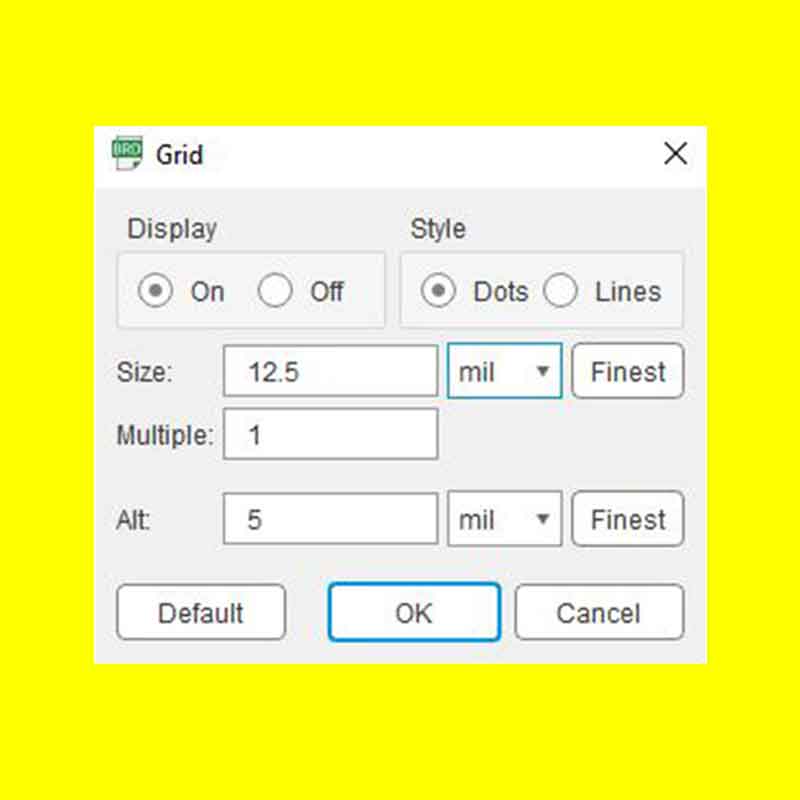
_how to activate the grid?
Go to VIEW>GRID
These are the values we used:
_how to activate the DESIGN RULES?
Go to TOOLS>DRC>click LOAD and add the file fabmodule.dru. If you don't have it, you can download it from HERE.
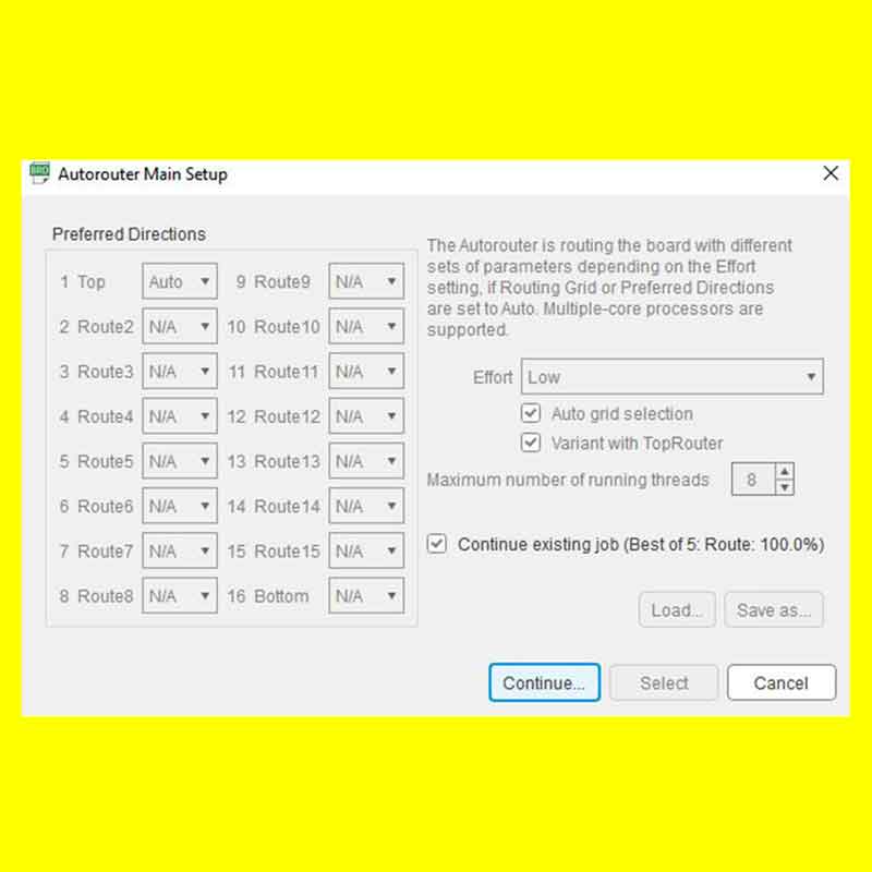
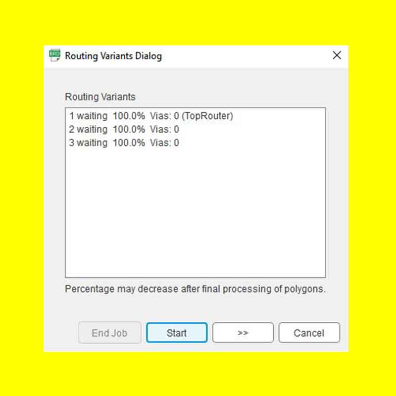
_how to run AUTOROUTER?
Go to TOOLS>AUTOROUTER
These will prompt a first window, leave all in N/A and choose CONTINUE.
Then another window will be prompted, here autorouter function will calculate several solutions and will
give you the accuracy in percentage (100% are no errors, but still make sure it works...). Run START,
and choose to end job when you select the option you think works best.
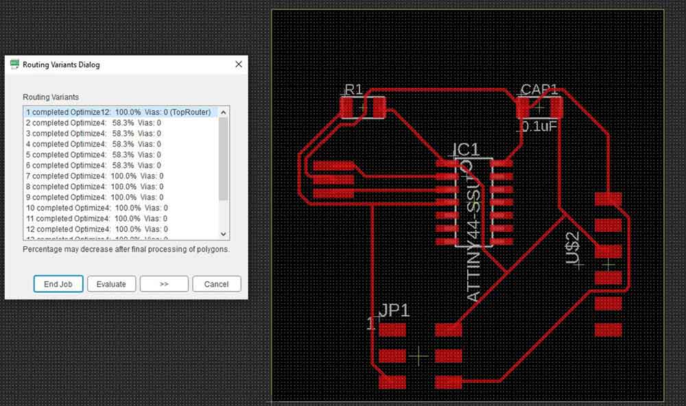
Example of AUTOROUTER on my MCU:
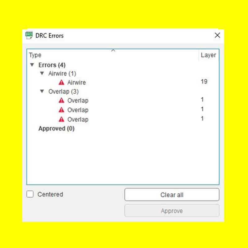
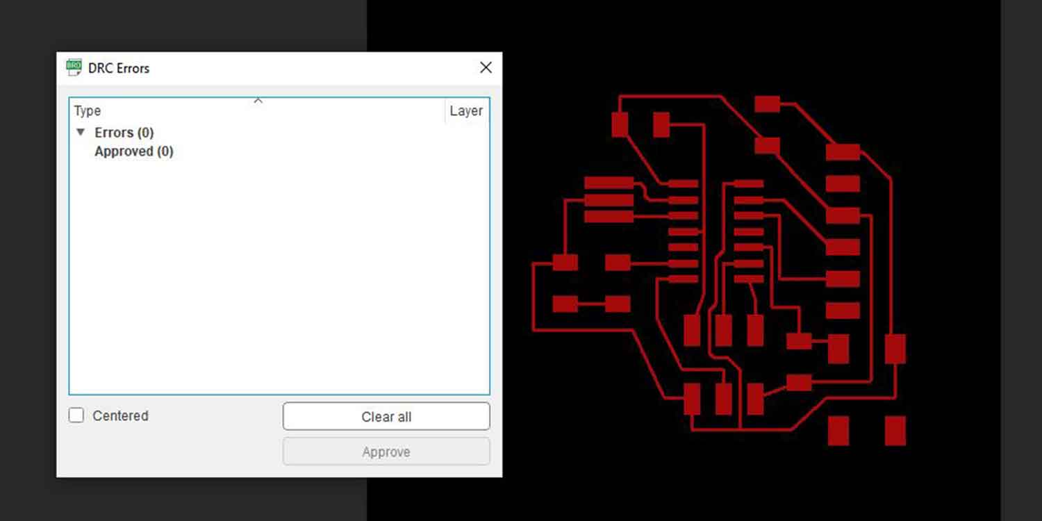
_how to run the DESIGN RULES?
Go to TOOLS>ERRORS
These will prompt a window and will show you all the erros you may have.
AIRWIRE is an error when there's no connection.
OVERLAP is when traces are overlaping.
Make sure you check this and fix any possible errors.
_how to turn off the LAYERS?
Go to VIEW>LAYERS SETTINGS
These will prompt a window, just leave TPO ACTIVE.
WHY? Because when we save this an image if we don't turn off all this layers, the tags will appear on
our board, and remember that for milling we only need the traces and nothing else.
This is my work in progress of the BOARD design:
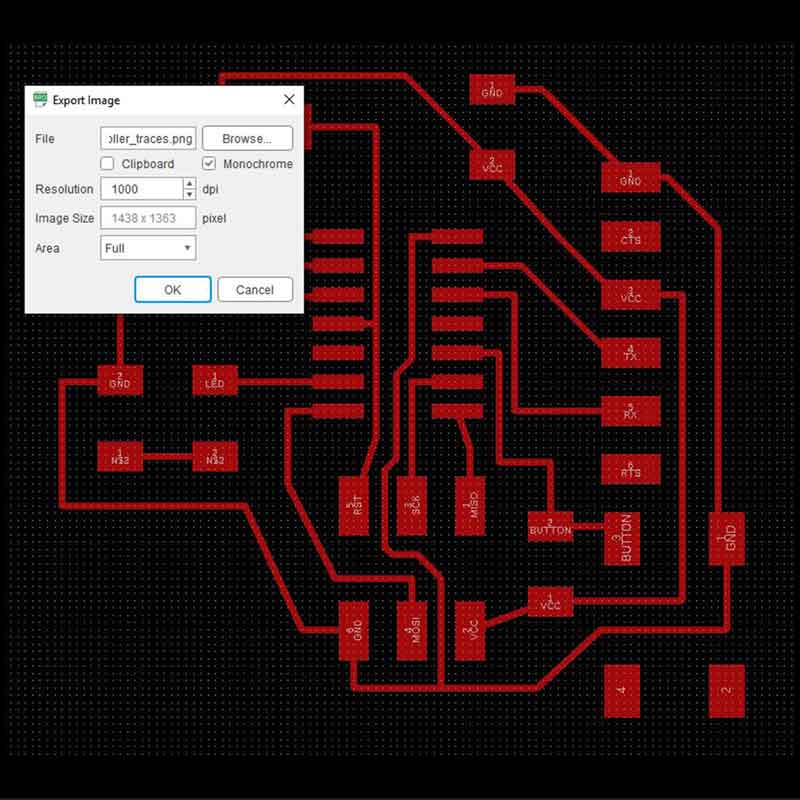
_EXPORT YOUR BOARD
After yu have run the DESIGN RULES and is good to go, export this as an image.
Go to FILE>EXPORT>IMAGE
Remember that the resolution MUST be 1000dpi, and choose MONOCHROME.
Note down the image size, so when you open it on PHOTOSHOP or any other software editing, you make sure
the size and the resolution are the same.
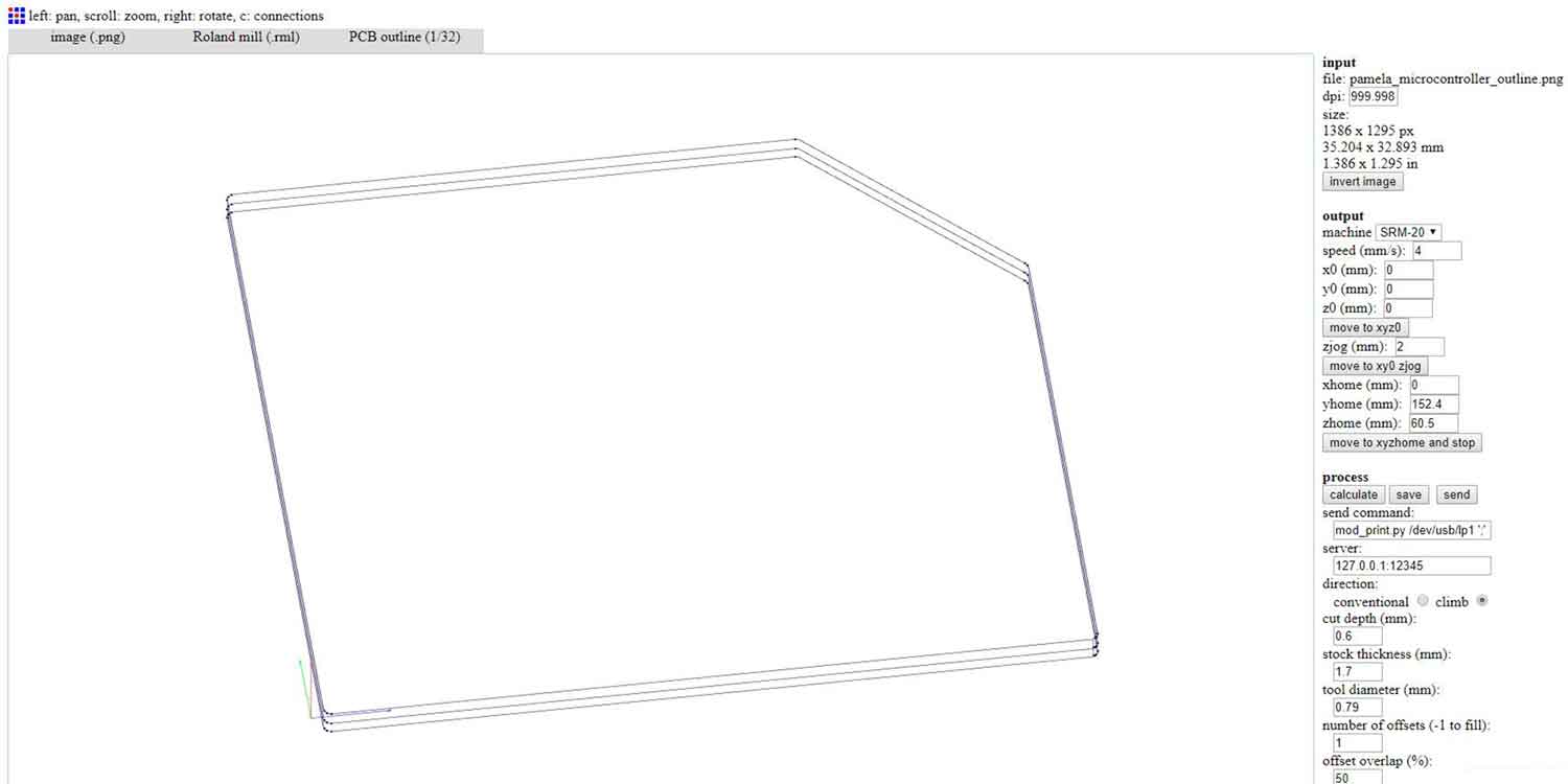
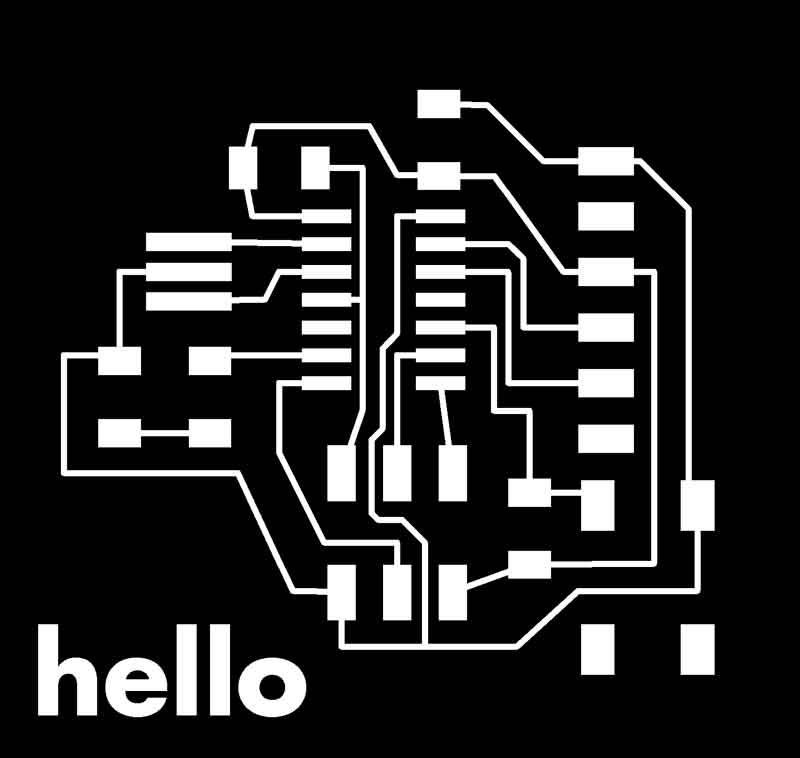
_CREATE TRACES AND OUTLINES
After having my board ready from EAGLE, I opened it on PHOTOSHOP to add the outline and some extra details:
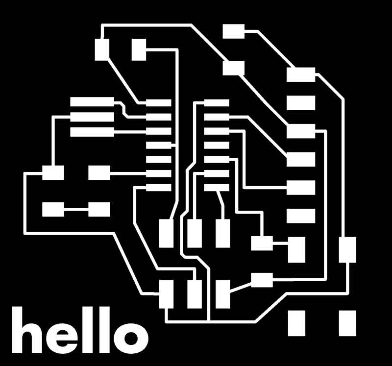
I then opened the PNG i generated into FABMODULES.
Here are both TRACES and OUTLINES files I created:
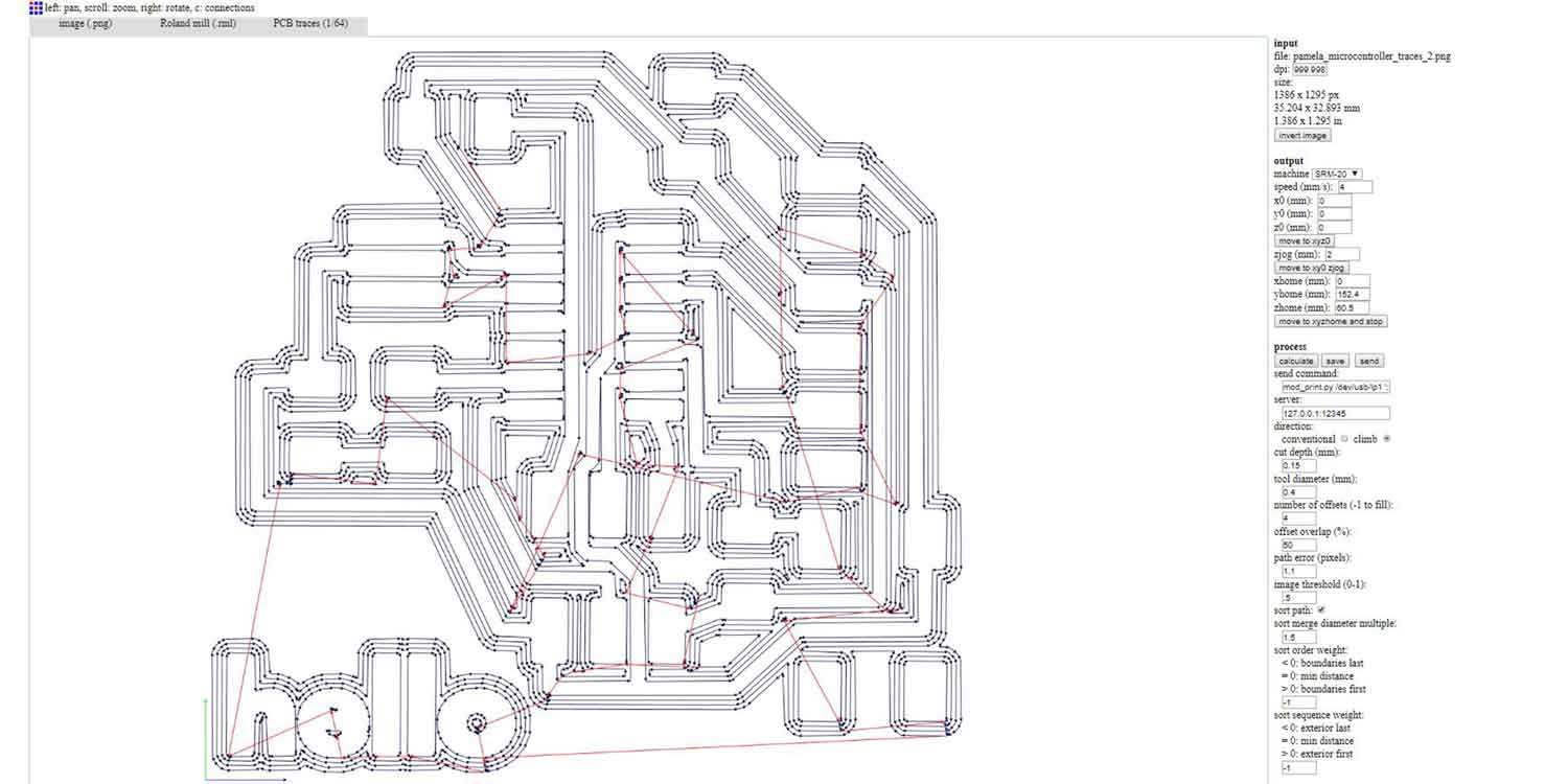
_MILLING PROCESS
_ERRORS & MISTAKES
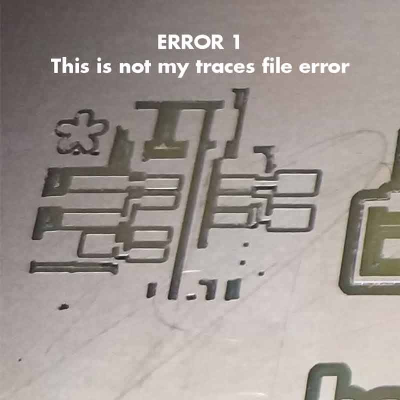
Until here it all seemed to be under control, but when I started the milling process, I had several issues...
ERROR 1 The first thing that happened to me was that after preparing the machine and setting up
the endmill, the XY and Z axis, I started the job and by mistake when I loaded my file to cut (in this
case the traces), I didn't realize that the software was choosing by default the previous work someone
else did that was on the DESKTOP, so when it started I saw the traces didn't seem to macth mines.
That's when I noticed it was not my design and it was the previous work someone did.
Unfortunately I had to waste that place on the board FR1 and I had to relocate the XY axis and restart
the job, this time I made sure it was my file.
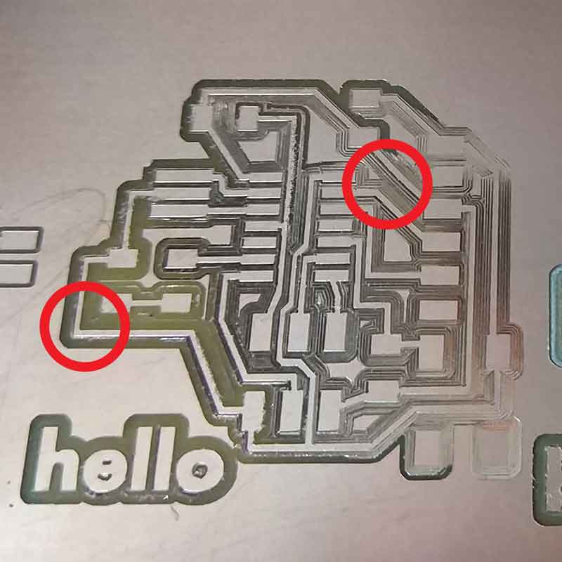
ERROR 2 After relocating X/Y/Z axis I restarted the job.
This time there was another error...
When the traces task was finished I noticed the cut between the traces was not deep enough and I also
noticed that certain areas the cut depth was clean and correct.
So I figured out the two issues, one was that the ENDMILL was probably dull. the second thing is that
maybe the FR1 board was not flat on the sacrificial layer, causing some areas to be deep and other
not.
ERROR 3 I had the idea to re-send the job but by mistake I moved the XY axis and I lost the
location of the previous task.
So I wasted that work that was already made in the FR1 board.
I learnt that if I reload my model I have to press XY to go back to origin and then I can press CUT.
ERROR 4 When I thought I was doing with the second iteration I made a mistake
After removing my model from the board, I proceed to clean it and remove with a knife the excess of
copper on the board.
But...the inevitable happened. I broke a trace with the knife, I took away a long piece of copper
accidentally.
So another wasted board, well I used it to practice my soldering so I did find a usage.
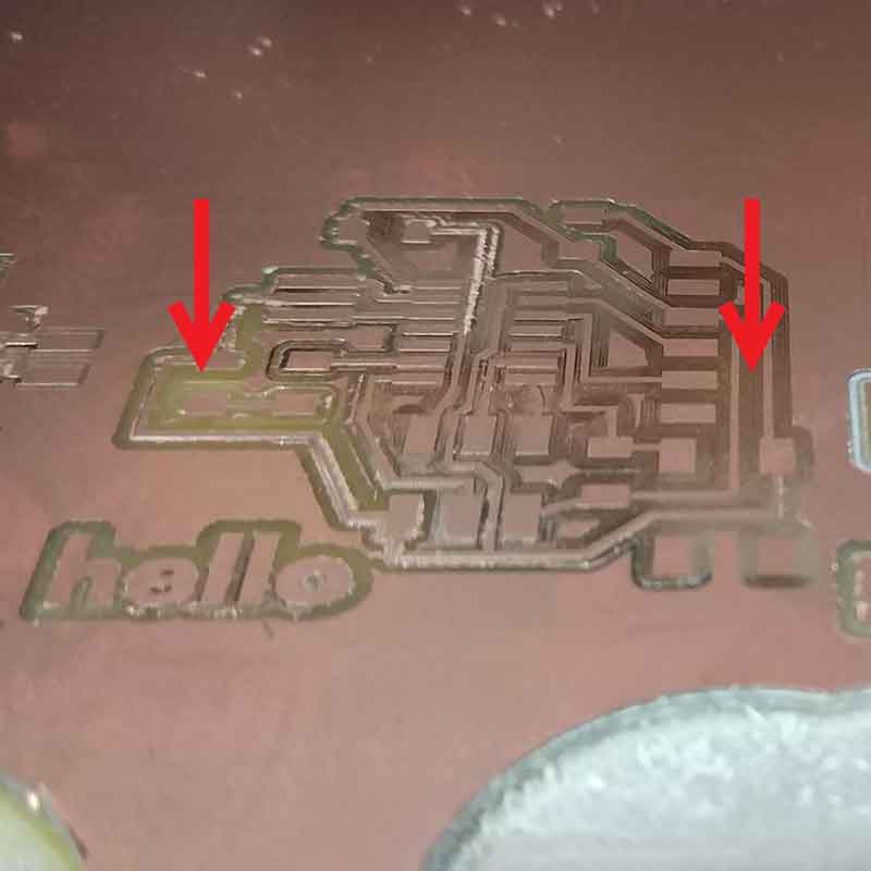
Ok, so at this point I was going to try for the third time cutting the board, but before that I decided
to modify the original board on EAGLE in order to have as less as possible copper to remove in the post
production.
So I re-arranged some components and their traces spacing.
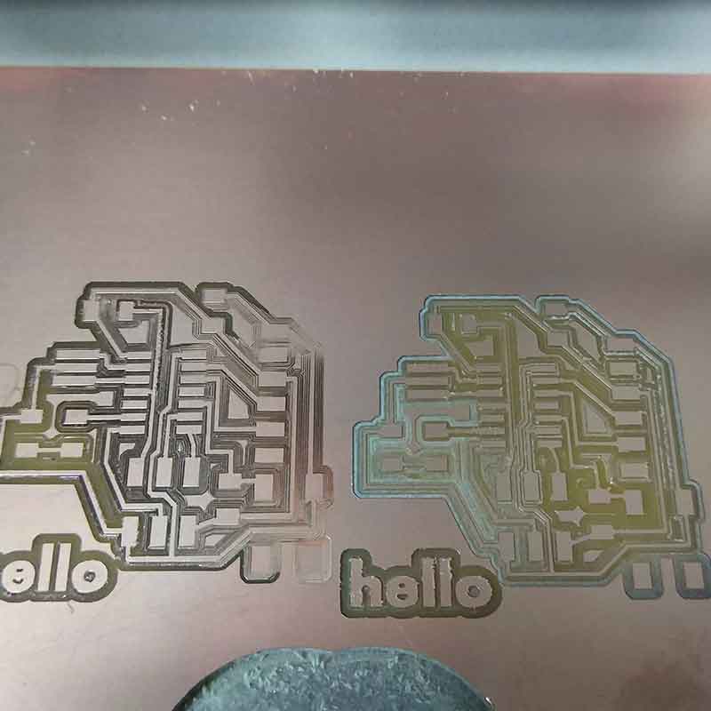
You can see the differences on the traces, the left one was the original model, the right one the new traces file:
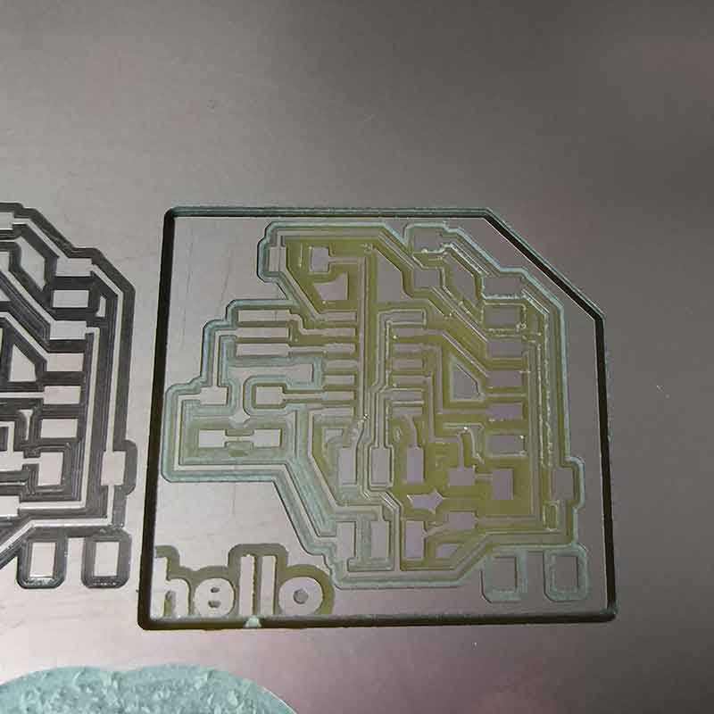
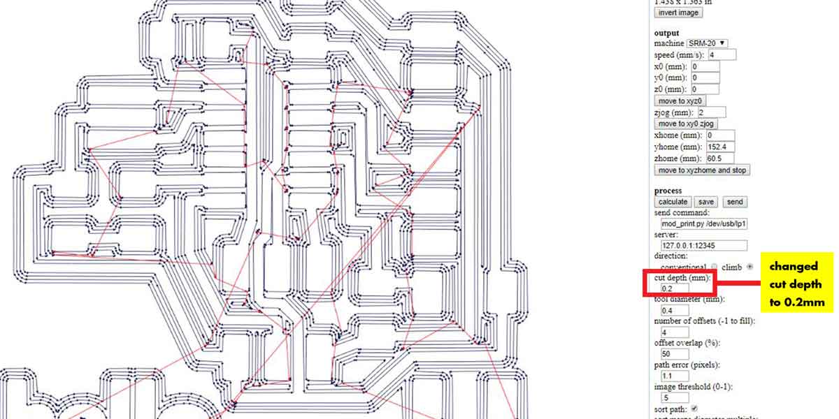
Then after learning my lesson that most of the endmills were dull, I modified the CUT DEPTH I in the .rml file by increasing the cut depth to 0.2mm.
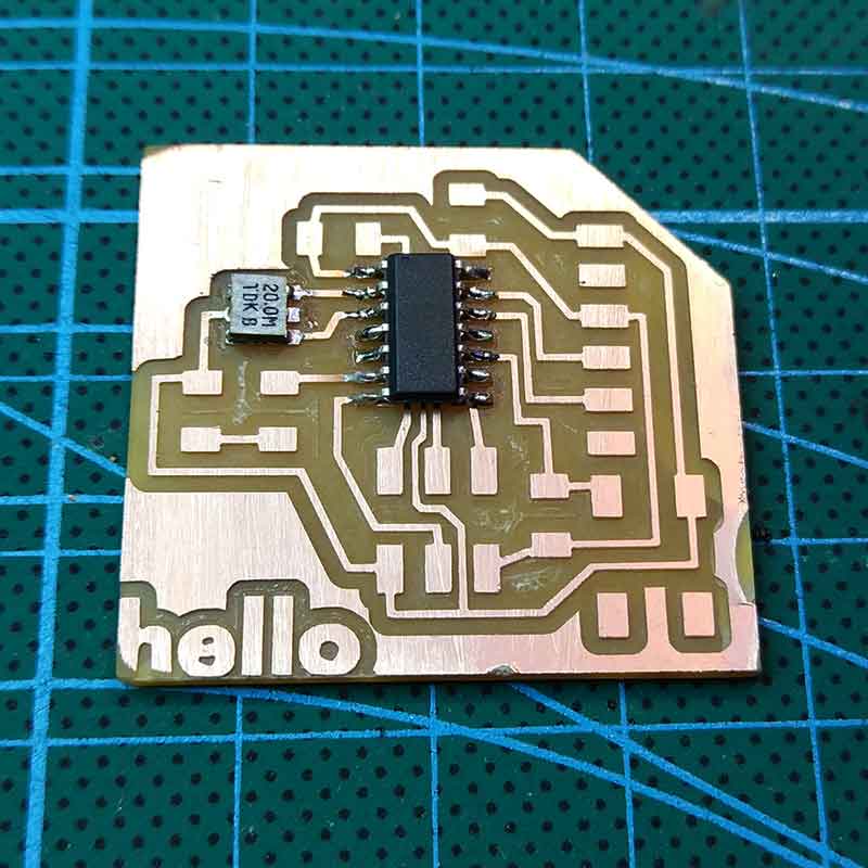
The third board was looking good!! changing the depth worked better (and also the endmill). Traces were clean and now I just had to run the OUTLINES task.
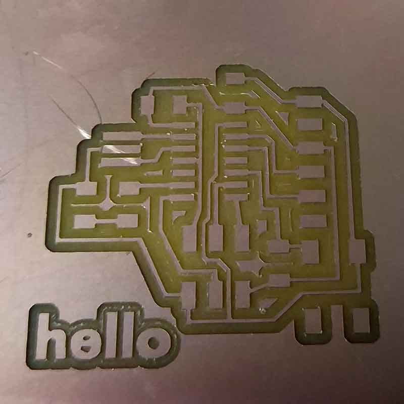
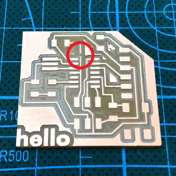
ERROR 5
But unfortunately when I removed it from the FR1 board, I realized that the OUTLINE cut was not deep
enought, meaning it didn't cut through a lot.
So when I removed my new board the edges were still un-cut, so I did afew "scars" behind when removing
it.
My guess here is that the board was definetly not flat on the sacrificial layer, so I should have either
increase the CUT DEPTH or redo the task lowering the Z axis or just changing the endmill and redoing the
OUTLINE task.
Either way it was my third iteration and it as quite late so I didn't think of doing any of the previous
things =(.
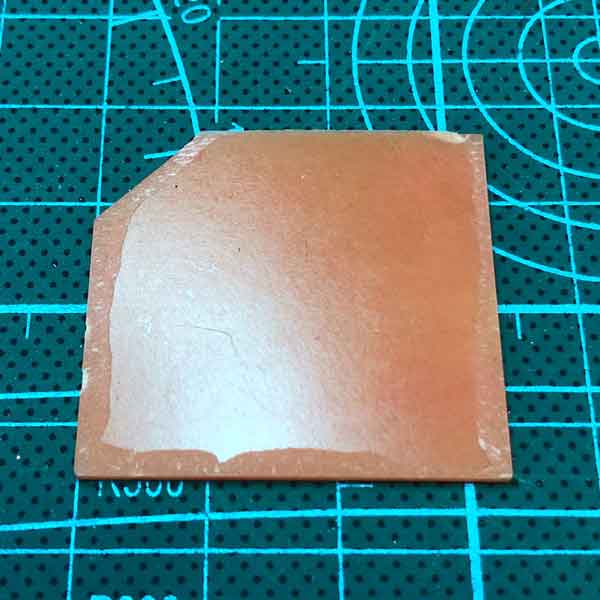
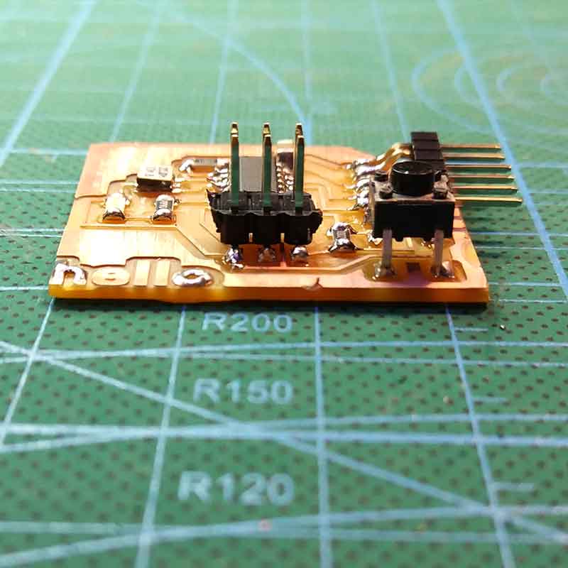
Now my board looks like Frankenstein from behind, but as I didn't want to waste material again I thought
of using this to solder the components.
After all, the copper layer is the important part on the FR1
board, and I wanted to see if it could work or not.
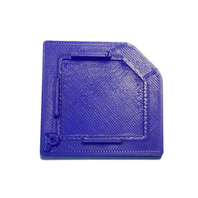
IDEAS
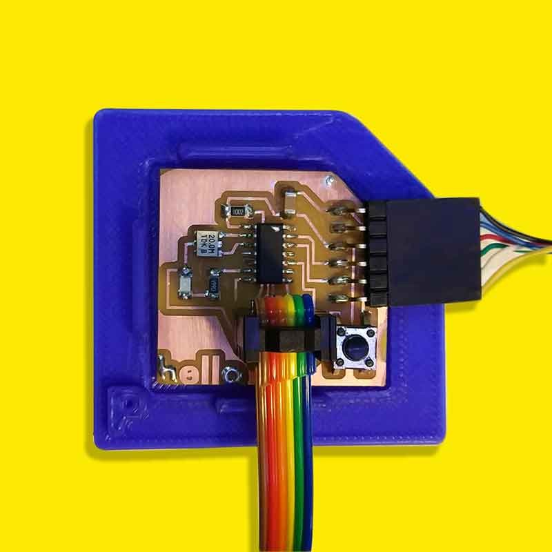
I plan to 3D print a case to cover the back of my board.
Here is the prototype I did to hold my MCU:

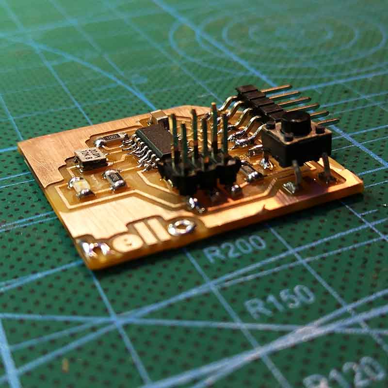
_SOLDERING THE COMPONENTS
I already mentioned above the type of components I would be using and why for this MCU, but I will do a
recap of the list:
_1 ATtiny44
_2xresistors of 10k Ohm
_1 capacitor 1uF
_1 FTDI pin
_1 SPI pin header
_1 crystal or resonator or 20MHz
_1 LED
_1 button
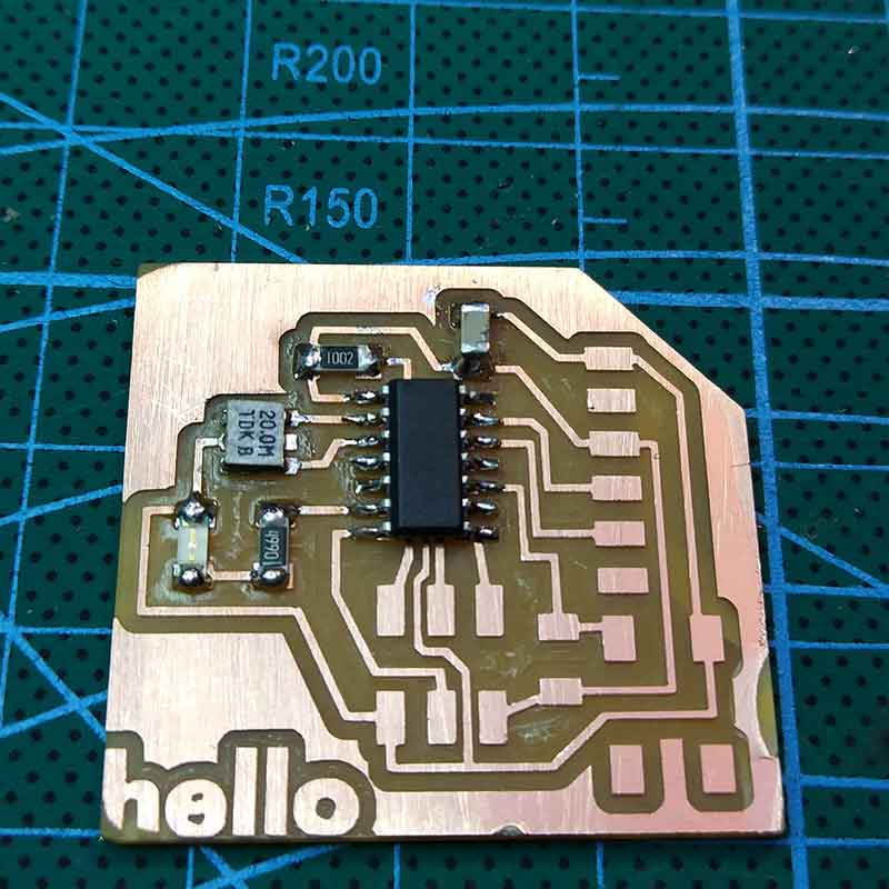
_1 resistor of 499ohm (in my calculation I did I just need a 180ohm resistor, but at the lab we only
have 100ohm and then jumps to 499ohm, although is more than needed, it should be fine)
_TIPS & TRICKS FOR THIS SOLDERING
This MCU compared to the FABISP has the traces closer and it has less space between the components, so you need more patience when soldernig it.
This is the order I followed to solder my components and some tips and tricks that were useful to me:
RESONATOR After a classmate finished with his soldering he told me that the
CRYSTAL/RESONATOR for him it was the hardest component to solder, as it only has attachment from
beneath.
So I decided I would begin from the CRYSTAL/RESONATOR. And yes it's a bit harder, but as this component
already has some soldering beneath, what worked was, placing the component on the board and then with
the iron tip heat a bit the copper trace and then the component, this would melt at least one strip of
the soldering on the resonator.
After that I added more soldering and tried to solder it as flat as possible.
I then soldered the ATtiny44, then the resistor 10k Ohm, then the capacitor (make sure you put enough soldering as this component is quite thick), then the other resistor of 499ohm, after that the LED, then the other resistor of 10kOhm.
And I left the tallest components for the end in the following order:
BUTTON The button we had was quite tall and from the legs it seemed to be more for "through
hole" component.
So I had to bend the legs of the button with tweezers and make them flat. (I advise you use some nice
thin and delicate tweezers for this task).
FTDI We only had vertical FTDI components at the lab, and we noticed that (at least on my board design and other classmates) when soldering the FTDI, it would inevitably touch the traces around it, as the pin legs are too long.
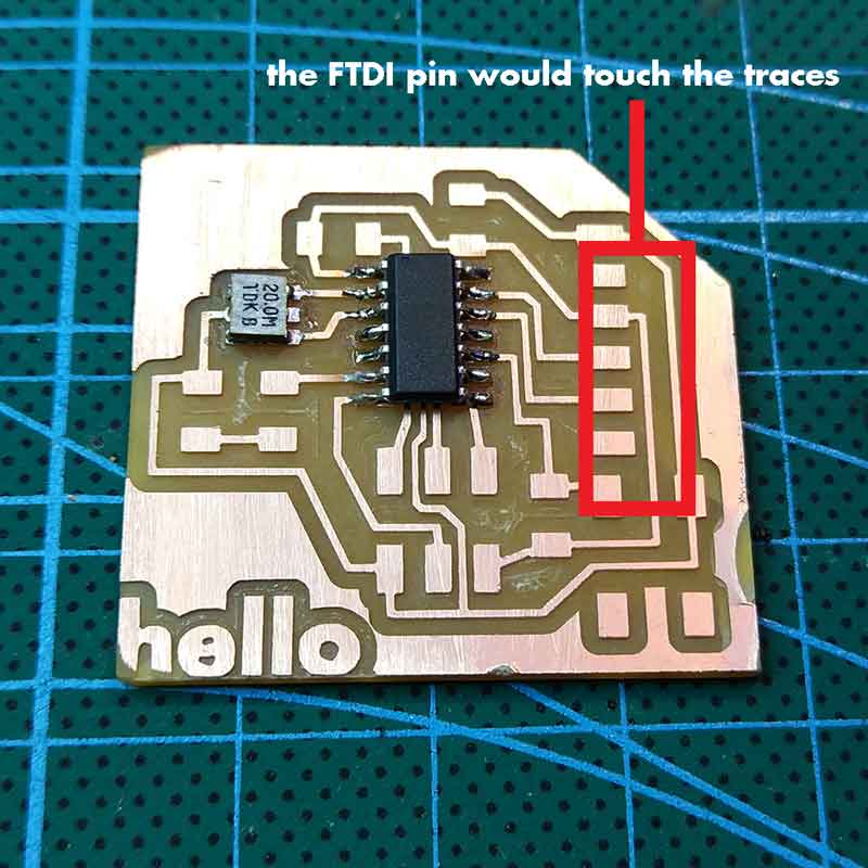
So what I did was to solder it flipped and I bent the legs of the component with some tweezers.
This would make the legs shorter and they would only touch the copper traces of their pins and not other
traces around.
I then proceed to solder the ISP pin head.
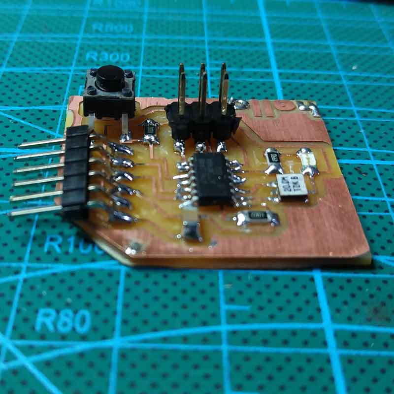
Here's the outcome of the soldering:
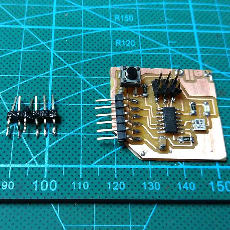
I checked all the components continutiy with the voltmeter and the soldering.
I noticed one of the legs from the FTDI pin was not touching perfectly the traces, altough there was
enough soldering, I decided to desolder this component, tweak a bit more the leg and solder it
again.
When I used the heat blower I melted the FTDI pin so I had to solder a new one, this time I carefully
bent the lengs using a better pair of tweezers.
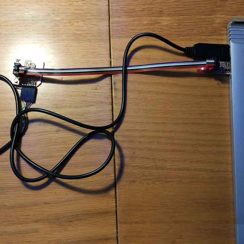
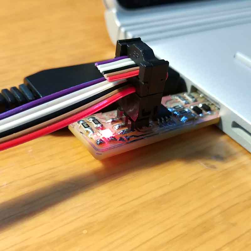
_TESTING THE ECHO HELLO BOARD
This was the most exciting part! a real conversation with my new MCU! but it was not that easy.
First thing was to check all the soldering, clean it with alcohol and checking the continuty.
After you make sure all the physical aspects work, go to your computer and install the "make" you will be
needing to program your new MCU.
You can find the files HERE in HOST COMMUNICATION and do SAVE LINK AS, or
download them directly from here:
hello.ftdi.44.echo.c
hello.ftdi.44.echo.c.make
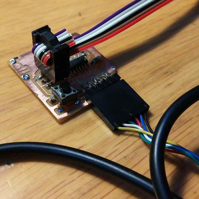
Then you have program your new MCU using an ISP, in this case I used the FABISP I did two weeks ago.
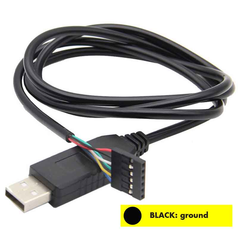
Connections are very important at this stage, and remember you will need a special cable, an FTDI USB
cable, so that you can connect the new MCU to a source of power (could be the same computer you are
using).
Make sure all the connections are correct in both cables, the ISP and the FTDI.
Once you have both the "make files" and all the connections under control, open your terminal (GitBash) and run this three commands:
make -f hello.ftdi.44.echo.c.make make -f hello.ftdi.44.echo.c.make program-usbtiny-fuses make -f hello.ftdi.44.echo.c.make program-usbtiny
On THIS LINK you can find the messages you should get when you run the above commands on GitBash.
*We noticed that the "SUDO" doesn't need to be typed if you are using Windows.
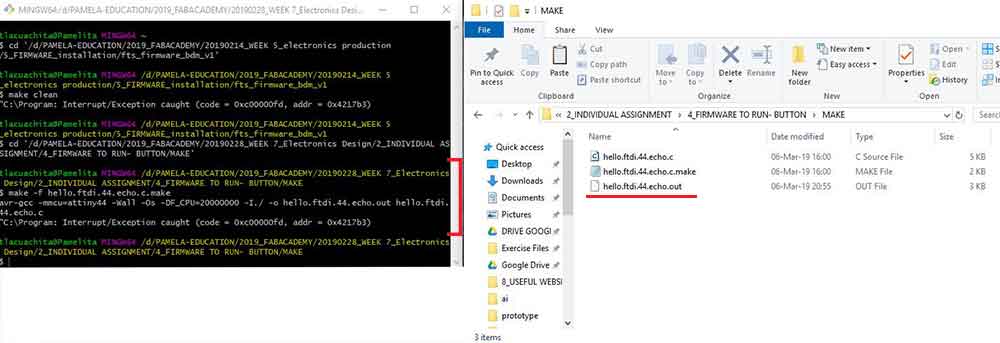
_ERROR in GITBASH "MAKE DOESN'T WORK"
I ran the commands I wrote above and...they didn't work out.
Below is a screenshot of the message I was getting at the beginning:
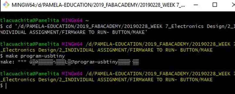
So I tried both connecting and re connecting all the cables, I cleaned my new MCU, I changed the ISP cable I tried with another FABISP that wasn't mine, but still it didn't work.
This is the message I was and still get whenever I try to run MAKE:
"C:\Program: Interrupt/Exception caught (code = 0xc00000fd, addr = 0x4217b3)"
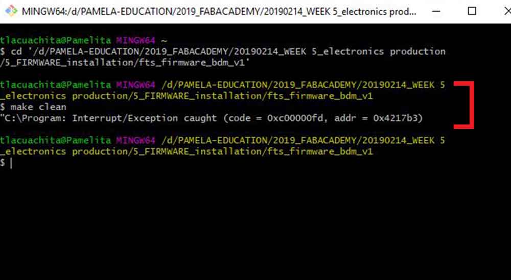
Somehow it creates an OUT file...
I kept reading and I couldn't find a solution to that error, the only thing I could find out is that maybe there is a problem with my computer, inside system properties in my environment variables, there could be a problem in the specified PATHS.
Here is a screenshot of my paths directory:
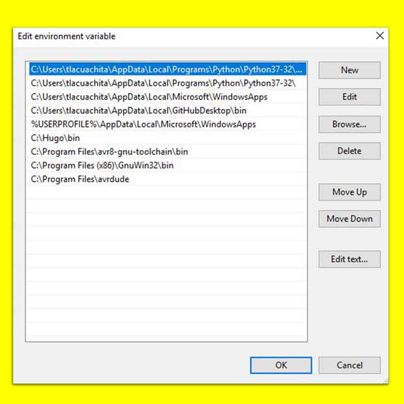
I read that sometimes the "()" could create issues on the paths, so I tried to uninstall GNU and reinstall it in my local disc C inside Program files not Program files (86), but still every time I ran MAKE command, I would get the same error shown above.
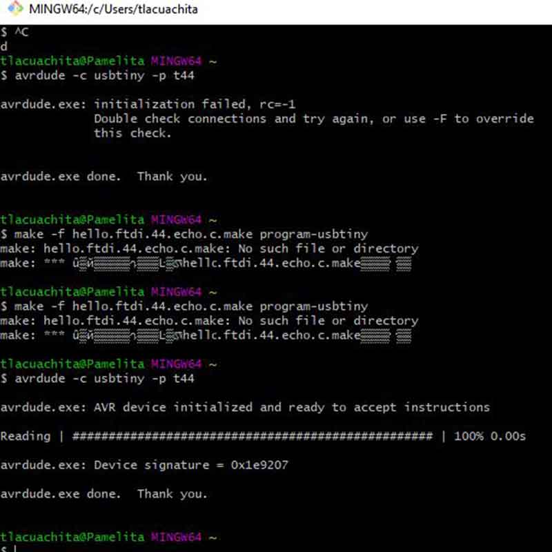
After being unable to solve this issue, I kept on reading other possible alternatives of how to program my board, and I found another student used another way for the simulation task.
I found this student's work useful (Xavi Klein). I tried running this command, it did work but then the next part where he programms it with Arduino, it didn't work out for me.
This is the command I ran:
avrdude -c usbtiny -p t44
_SUCCESSFUL OPERATION!
I thought of using another alternative, as one of my classmates was succesfull with the make and make fuses commands, I asked his FABISP borrowed to give it a try once again, I also changed both the ISP and FTDI cable and I tried it from his computer.
This time it worked!!!! here are the commands ran in GITBASH:
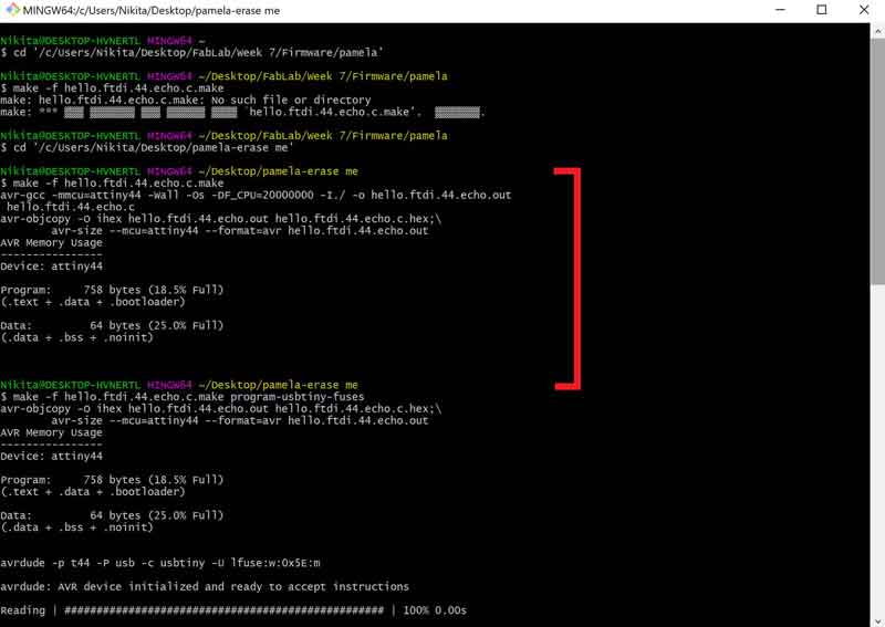
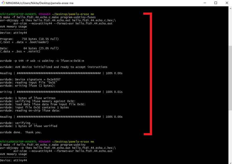
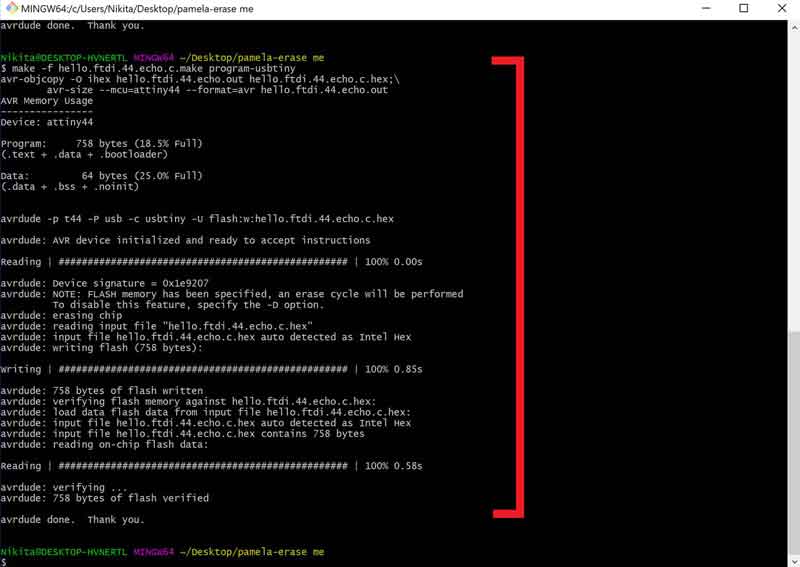
After runnig this command the new MCU is ready for programming.
I used ARDUINO to test the HELLO ECHO response.
After you download and install ARDUINO you have to do the following:
1_.JSON, go to FILE> PREFERENCES> ADDITIONAL BOARDS MANAGER URLs, and paste this link:
https://raw.githubusercontent.com/damellis/attiny/ide-1.6.x-boards-manager/package_damellis_attiny_index.json
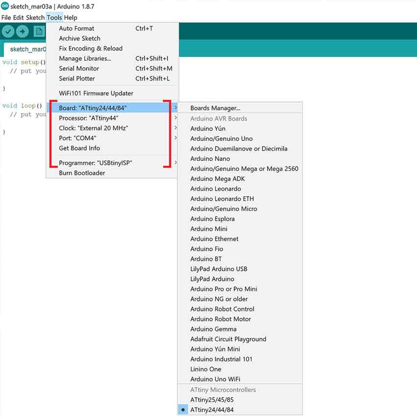
2_INSTALL ATtiny package, go to TOOLS> BOARD> BOARDS MANAGER> inside "filter your search look for attiny by David A. Mellis, click on it and it will install it automatically.
After doing this settings, you have to configure the type of board you are using inside TOOLS menu (this
configuration will depend on the type of MCU you are using and its components).
For this type of MCU you need to choose the following:
The PORT, if it doesn't appear you should install the drivers in your computer. HERE.
If you are installing at this point the COM port drivers, it's better if you close and re-open ARDUINO
once you are done.
After you choose the above settings, you have to run BURN BOOTLOADER.
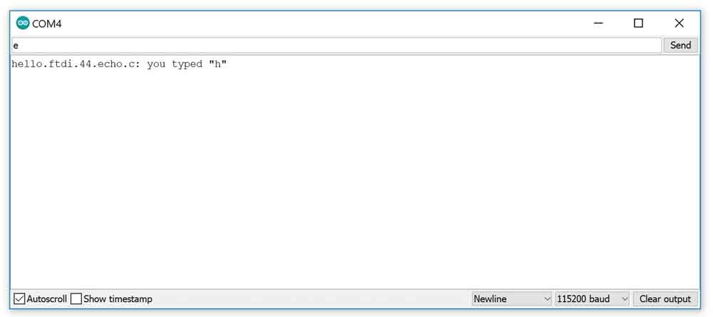
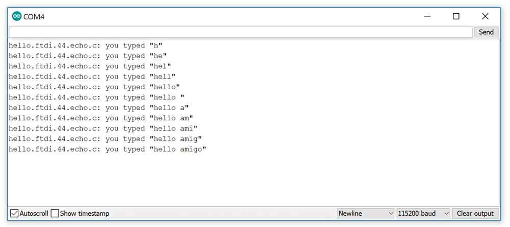
Now open TOOLS > SERIAL MONITOR, a window will be prompted, here you can start typing words, and your new MCU will reply you!!!!!!!!
And here is the most exciting converstaion I had during this week's assignment!
_NOTE
If you can't see any letters but instead you see weird signs, it's probably becuase your "baud" (it's
a unit of transmission speed equal to the number of times a signal changes state per second-source
from internet).
In this case the baud I used was 115200 bauds.
_BLINK SIMULATION
Using ARDUINO IDE I loaded a basic program to make the LEDs blink.
The video and documenation I moved it into week 9_embedded programming.
_DOWNLOAD FILES
Here you can find the files of the week, just click the link that will prompt a window to Sketchfab and proceed to dowload the files:
_EAGLE schematic
_EAGLE board
_MCU BOARD traces file PNG
_MCU BOARD outline file PNG
_MCU BOARD traces file RML
_MCU BOARD outline file RML