Designing
Summary
- Design Output Microcontroller Board
- Creat New Project & Sketch KICAD
- Import Fab Library
- Import Components
- Connect Components
- Give Compoents correct name and value
- Annotate the design
- Assign Footprint to Symbols
- Generate Netlist
- Open Pcb New
- Read in Generate netlist
- In Pcb New Set Design Rules (Setup -Design Rules)
- Rearrange Components and Make Traces
- Place your Auxillary Axis
- Plot Layers
- Flatcam
- Tool dia 0.4
- Cutz -0.1
- Travel Z 2.5
- Feed Rate 0.3
- Spindle speed 1000
- Passes 2
- Solder Output Microcontroller Board
- Programming Output Microcontroller Board
Designing
For input week I decided to make a microcontroller board using the attiny45 microcontroller and for my sensors I choose to use the phototransistor as my analogue sensor and the dht sensor for my digital input sensor.I also added the avrisp for programming my board and the 6 pin header for connecting my htdi cable to read from serial. Component list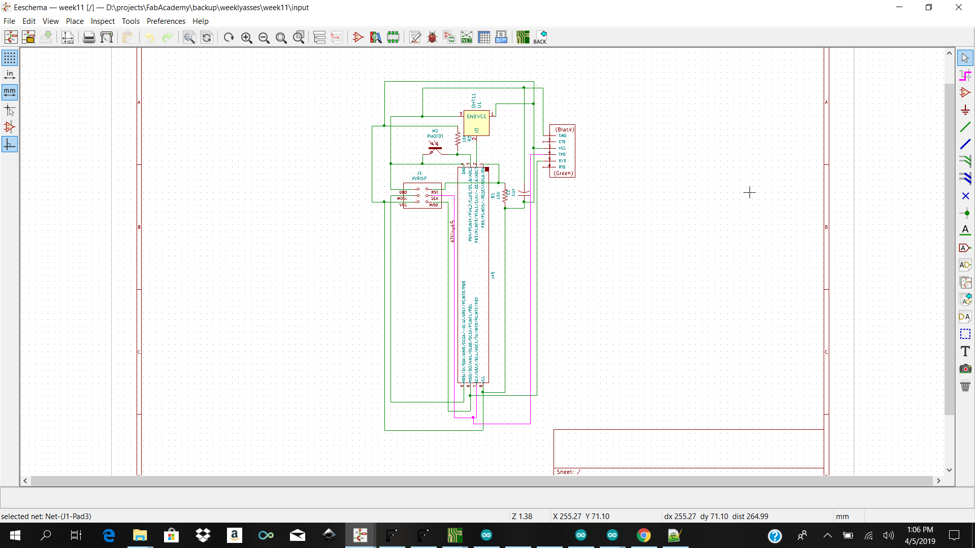 I then went ahead and started making my skematic in Kicad. I made a new project and started selecting my components from the fab library. I found most of my components from the fab library but I had to add my own library for the dht sensor. After making my schematic in kicad I went ahead and anotate to check if I had my tags labeled correctly.
After that I went ahead and selected assign footprint to pcb and added my footprint. I had an issue with my dht library which had 1 2 4 instead of 1 2 3 so I had to change the labels and save it as another library called sensor 2 then I selected that footprint for my dht sensor. I then selected on Generate netlist and imported my netlist for Pcbnew.
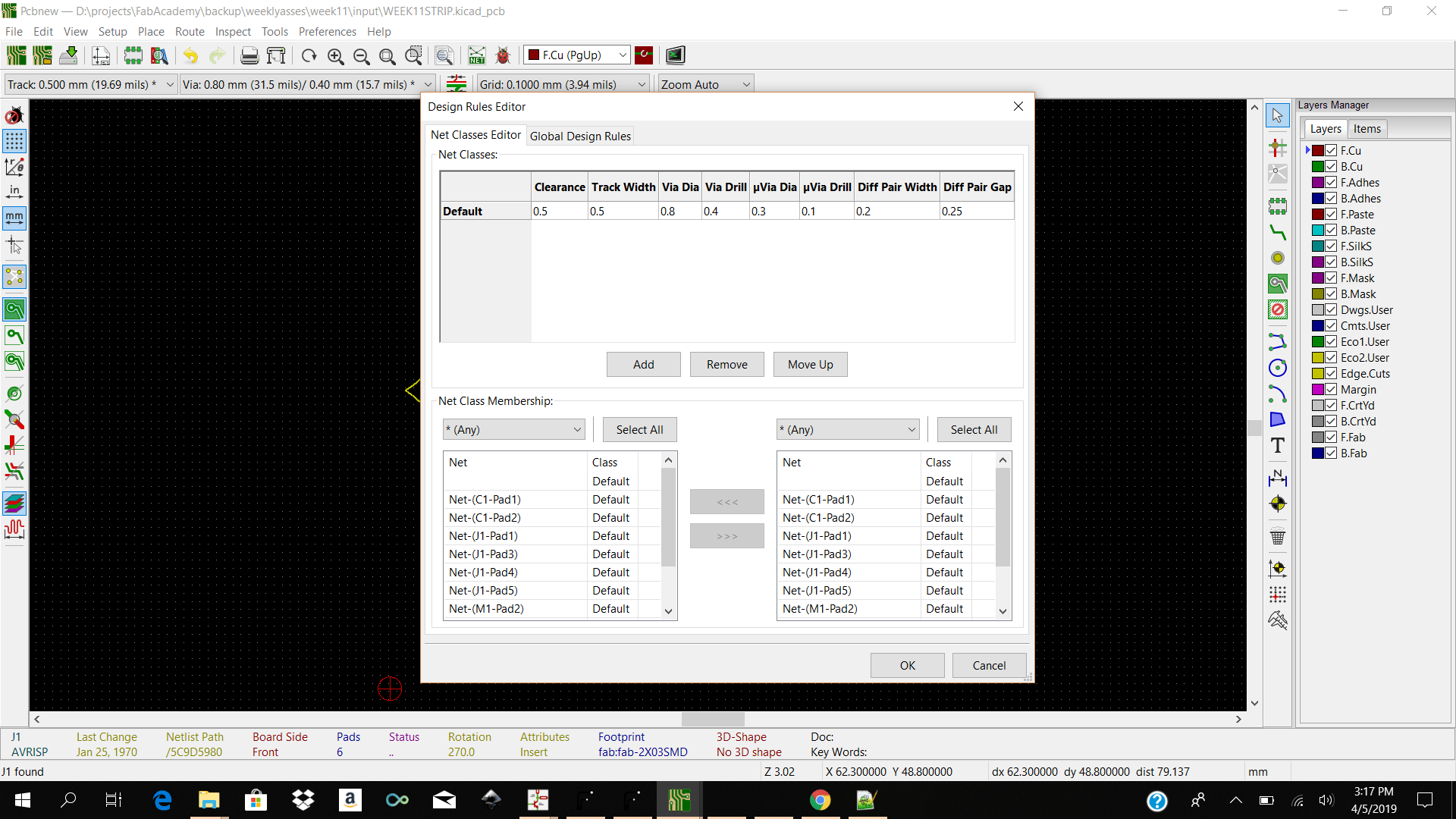
I then went ahead and choose my design rules from Setup → Design rules
My clearance was set to 0.2 and my track width was 0.35 because I was using a 0.4 mm bit for milling my pcb
I then went ahead and started making my skematic in Kicad. I made a new project and started selecting my components from the fab library. I found most of my components from the fab library but I had to add my own library for the dht sensor. After making my schematic in kicad I went ahead and anotate to check if I had my tags labeled correctly.
After that I went ahead and selected assign footprint to pcb and added my footprint. I had an issue with my dht library which had 1 2 4 instead of 1 2 3 so I had to change the labels and save it as another library called sensor 2 then I selected that footprint for my dht sensor. I then selected on Generate netlist and imported my netlist for Pcbnew.
I then went ahead and choose my design rules from Setup → Design rules
My clearance was set to 0.2 and my track width was 0.35 because I was using a 0.4 mm bit for milling my pcb
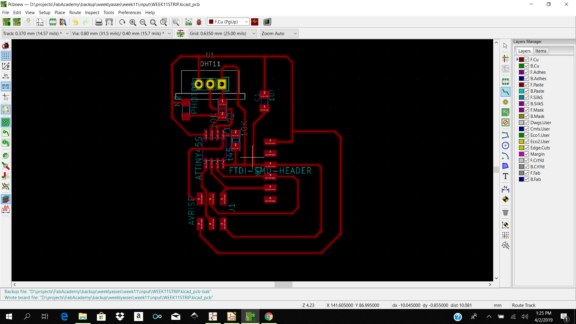
 I had a stressful time routing my board initially but with the help of my local instructor I finally got the hang of it.
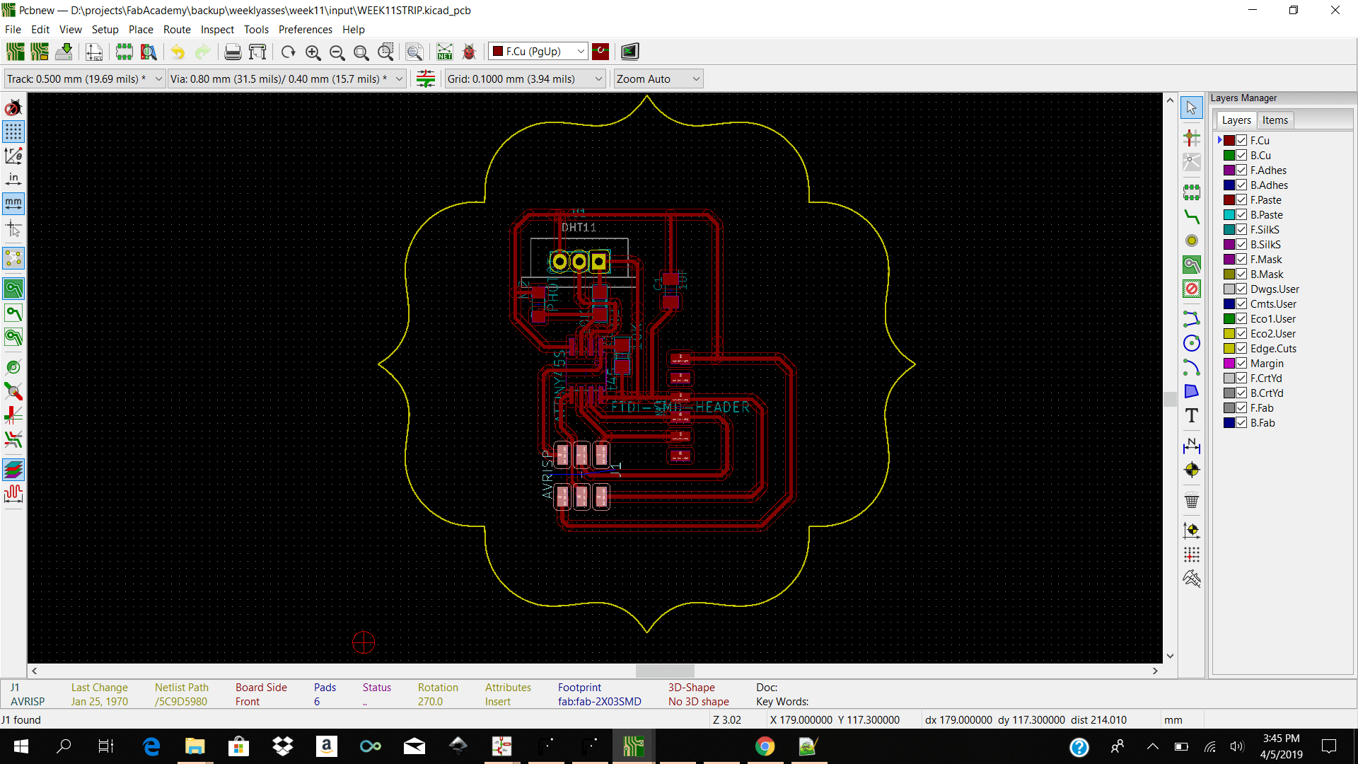
 This week I wanted to try something new with my pcb design.Since I got the hang of working with kicad I decided to add a custom edge cut to my board.
I found a silhouette png which I liked from the internet I downloaded it and open it using Inkscape I then bittrace it using inkscape and resize it then export it as dxf. I then imported that dxf into librecad select the object and select explode to explode the traces.
I then saved my file from librecad to dxf and imported it as edgecut into kicad.The reason why I had to do so many steps is because when just bitracing my image in inkscape and importing it into kicad kicad does not detect all the lines.
This week I wanted to try something new with my pcb design.Since I got the hang of working with kicad I decided to add a custom edge cut to my board.
I found a silhouette png which I liked from the internet I downloaded it and open it using Inkscape I then bittrace it using inkscape and resize it then export it as dxf. I then imported that dxf into librecad select the object and select explode to explode the traces.
I then saved my file from librecad to dxf and imported it as edgecut into kicad.The reason why I had to do so many steps is because when just bitracing my image in inkscape and importing it into kicad kicad does not detect all the lines.
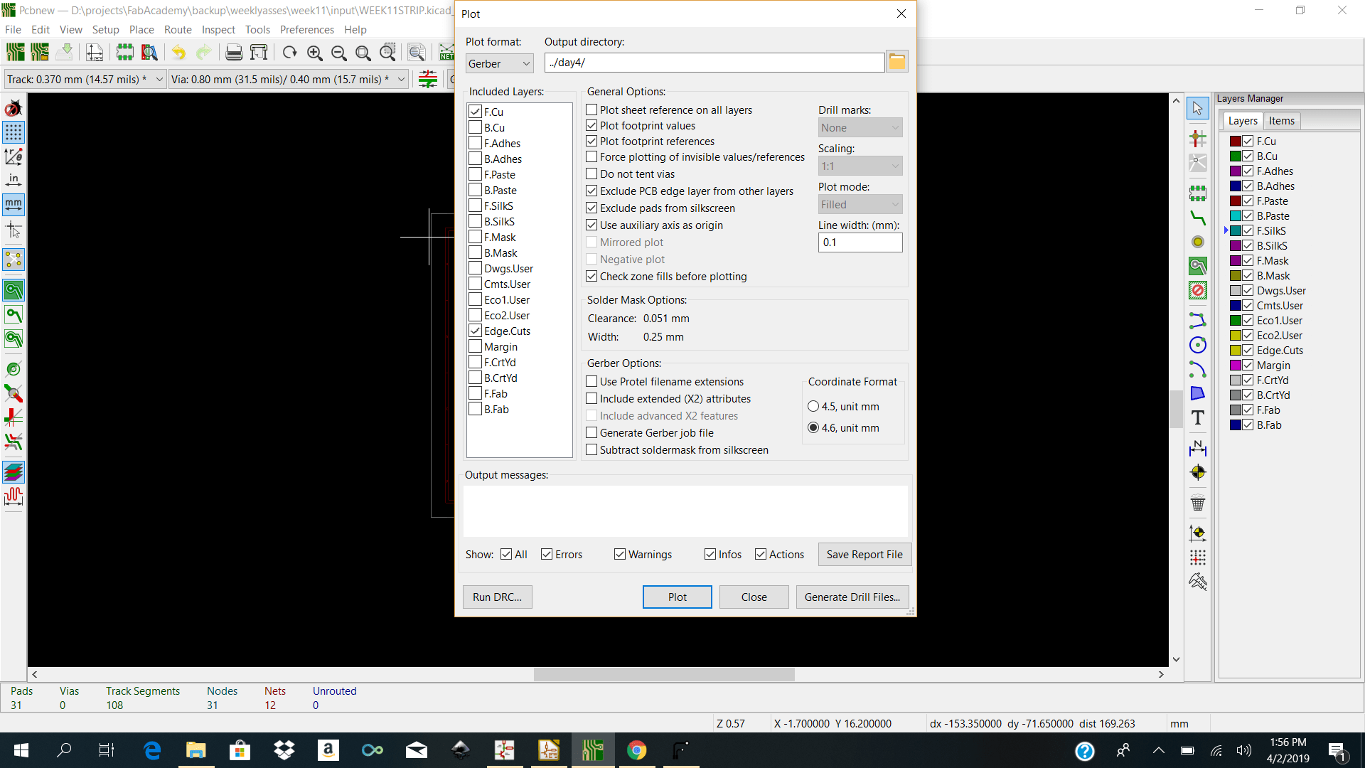
 After importing my edge cut into kicad I then determined my auxillary origin using the place the auxiliary origin icon and went ahead and plot my layers. When plotting I checked off front and edge cut and if i wanted to get the file for making the holes in my pcb for the dht sensor I needed to select generate drill file. I did not want to make the hole in my pcb so I did not select generate drill files.
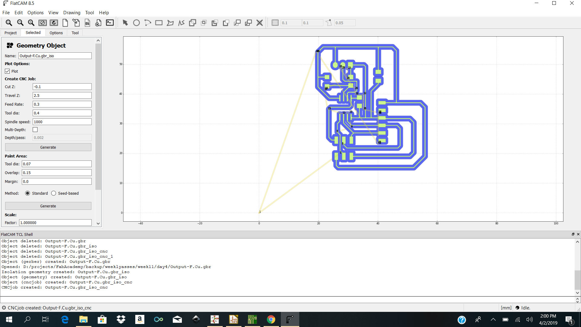
 After generating my gerber files I then went ahead and open flatcam to add my parameters.
For the front cut I selected
Tool dia - 0.4
Passes -2
Cut Z -0.1
Travel Z- 2.5
Feed Rate 0.3
Spindle speed 1000
After generating my gerber files I then went ahead and open flatcam to add my parameters.
For the front cut I selected
Tool dia - 0.4
Passes -2
Cut Z -0.1
Travel Z- 2.5
Feed Rate 0.3
Spindle speed 1000
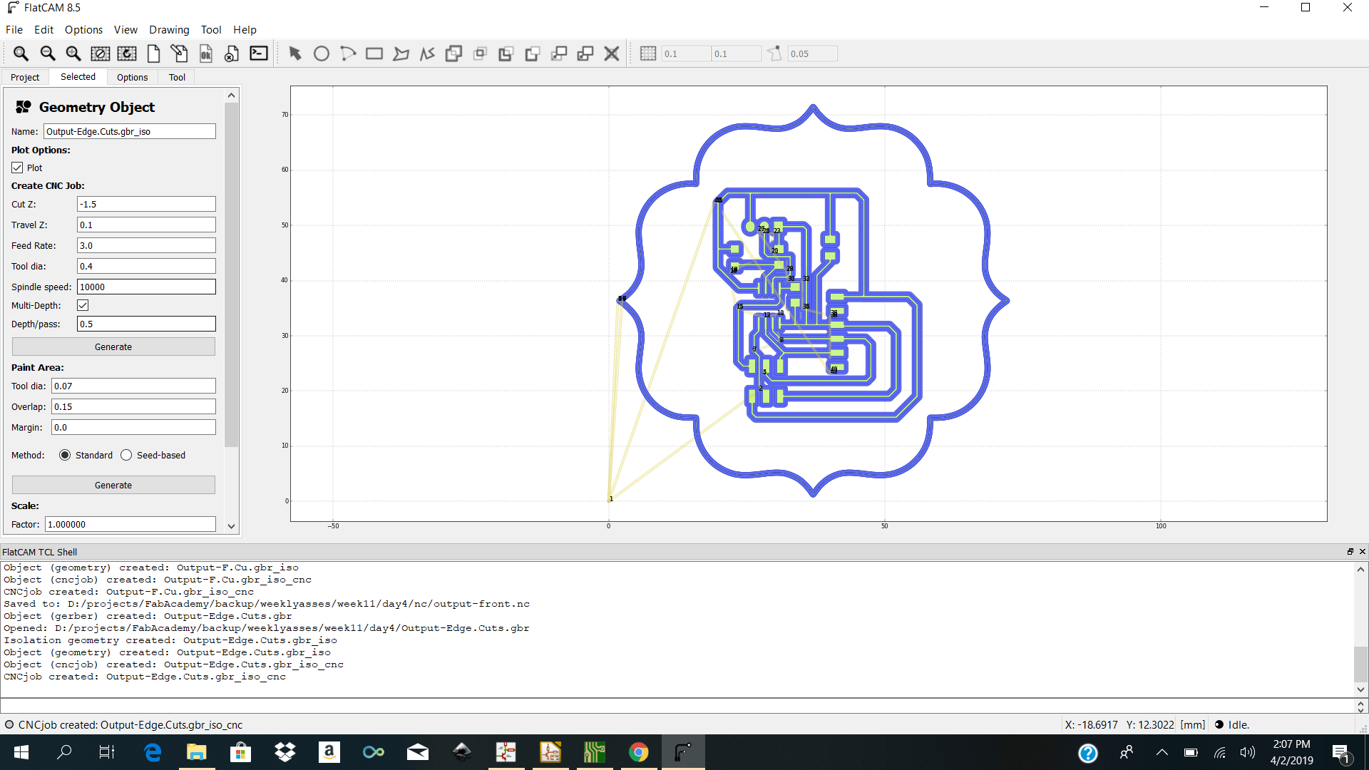
 Edge Cut
Tool dia - 0.4
Passes -1
Cut Z - -1.5
Travel Z- 0.1
Feed Rate 3.0
Spindle speed 10000
Multip dept checked
Depth/Passes 0.5
Edge Cut
Tool dia - 0.4
Passes -1
Cut Z - -1.5
Travel Z- 0.1
Feed Rate 3.0
Spindle speed 10000
Multip dept checked
Depth/Passes 0.5
 I then went ahead and generated my nc files for importing into winpc nc to control the stepcraft to cut the pcb.
Machining
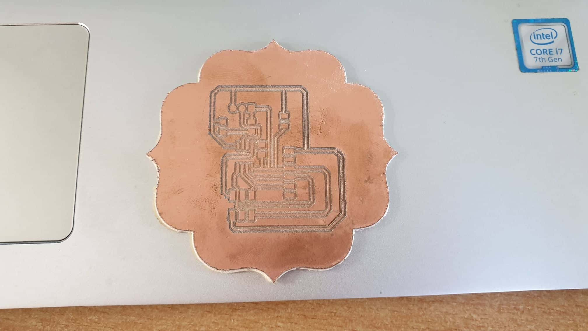
I then went and physically placed my copper plate onto the stepcraft base plate using double sided tape and imported my front cut.nc file into winpcnc. The parameters I had to keep in changer were add under Parameters Origin of coordinates Misc.parameters Zero point Import Formats Invert z axis I then went ahead and jog the mill to my preferred x y and z positions. After I double checked that my x y and z positions were good I clicked on start and milled my board out.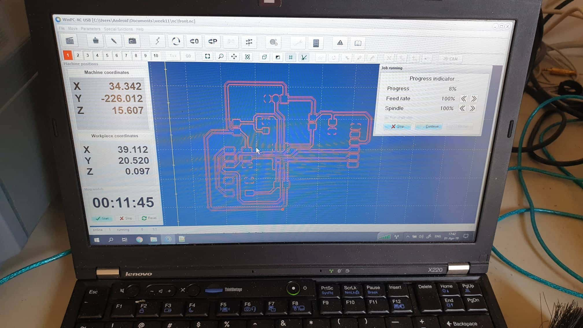 note: the image above is a screenshot of my previous trial of my board not the final version I forgot to make a screenshot of the final board. Below is the final board when finished cutting.
When my front cut was finished I did the same for my edge cut.I uploaded my edgecut.nc file then made my zero position was correct and press start.
note: the image above is a screenshot of my previous trial of my board not the final version I forgot to make a screenshot of the final board. Below is the final board when finished cutting.
When my front cut was finished I did the same for my edge cut.I uploaded my edgecut.nc file then made my zero position was correct and press start.
Soldering
Soldering
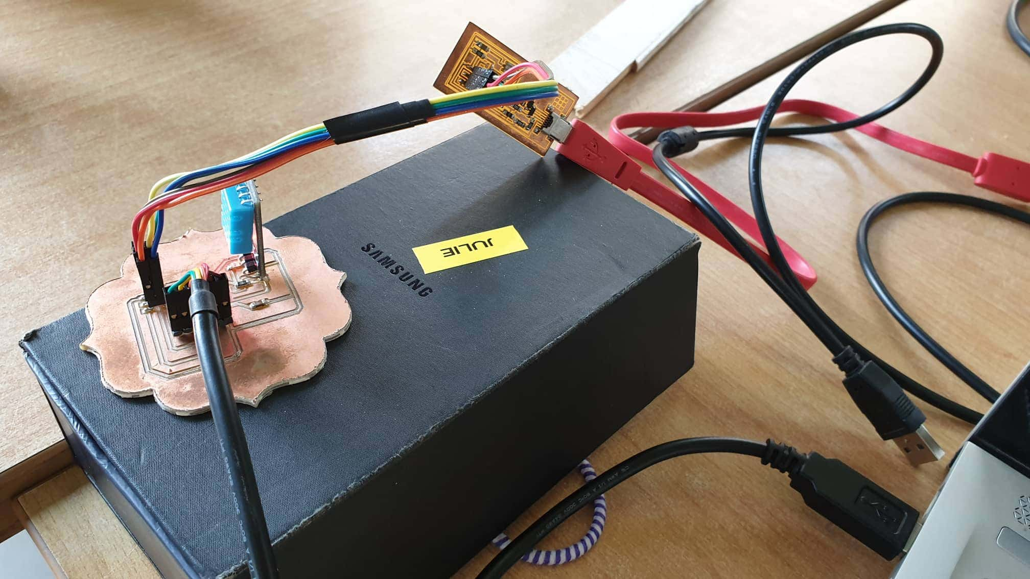
After I got my pcb milled I took the multimeter and checked my connections if all that needs to be connected is connected and all the does not need to be connected is not. I was so happy that all the connections were good. I then went ahead and gathered my smd components and sensors and soldered my board. Some things I had to keep in when soldering my pcb was that the phototransistor green connection was not the connection for gnd like the led instead it was the opposite.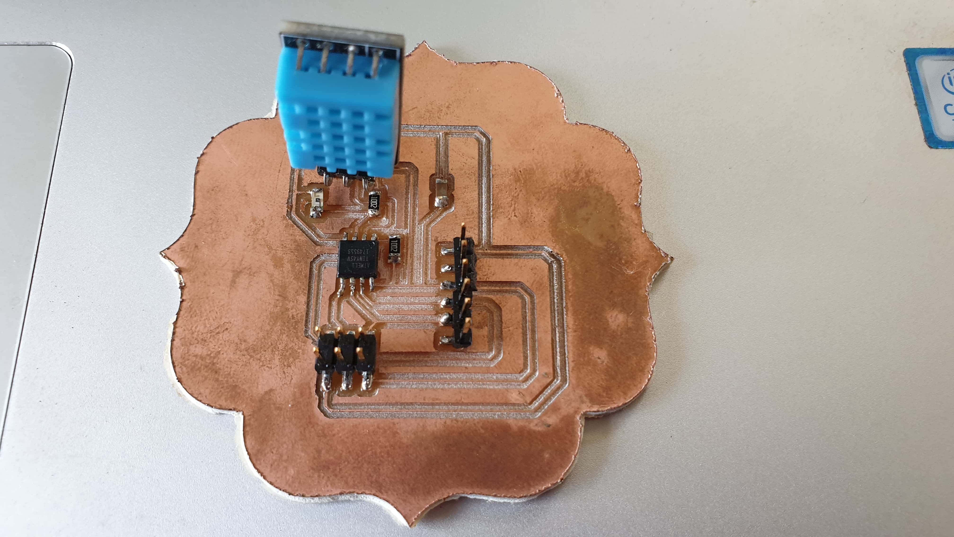
Programming
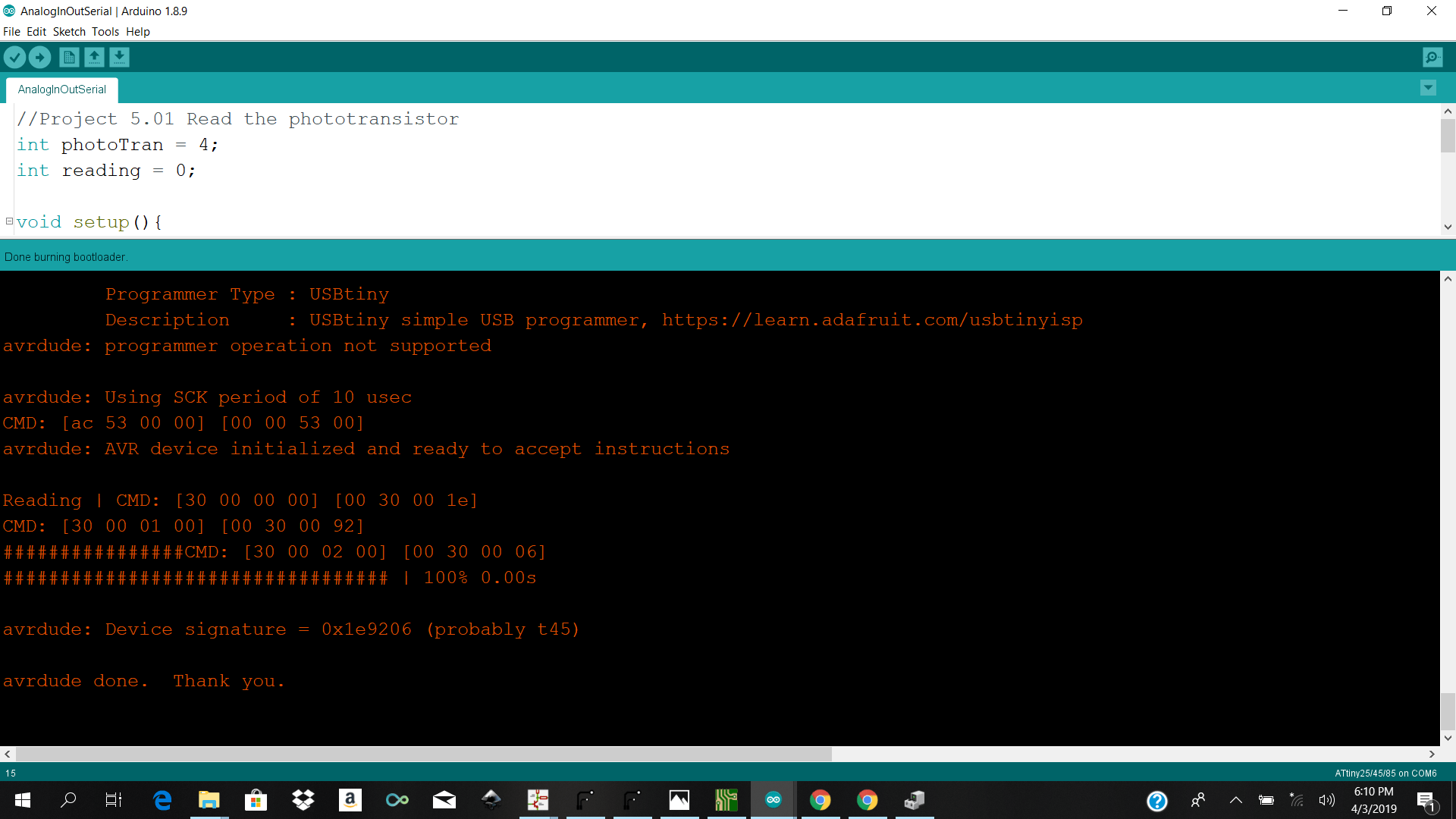
After soldering my board I went ahead and programmed it. The first thing which I had to do was to connect my input board to my fab isp and connect the fab isp to my computer and burn the bootloader using the arduino ide. I had already have the attiny core library installed from the previous week so I selected the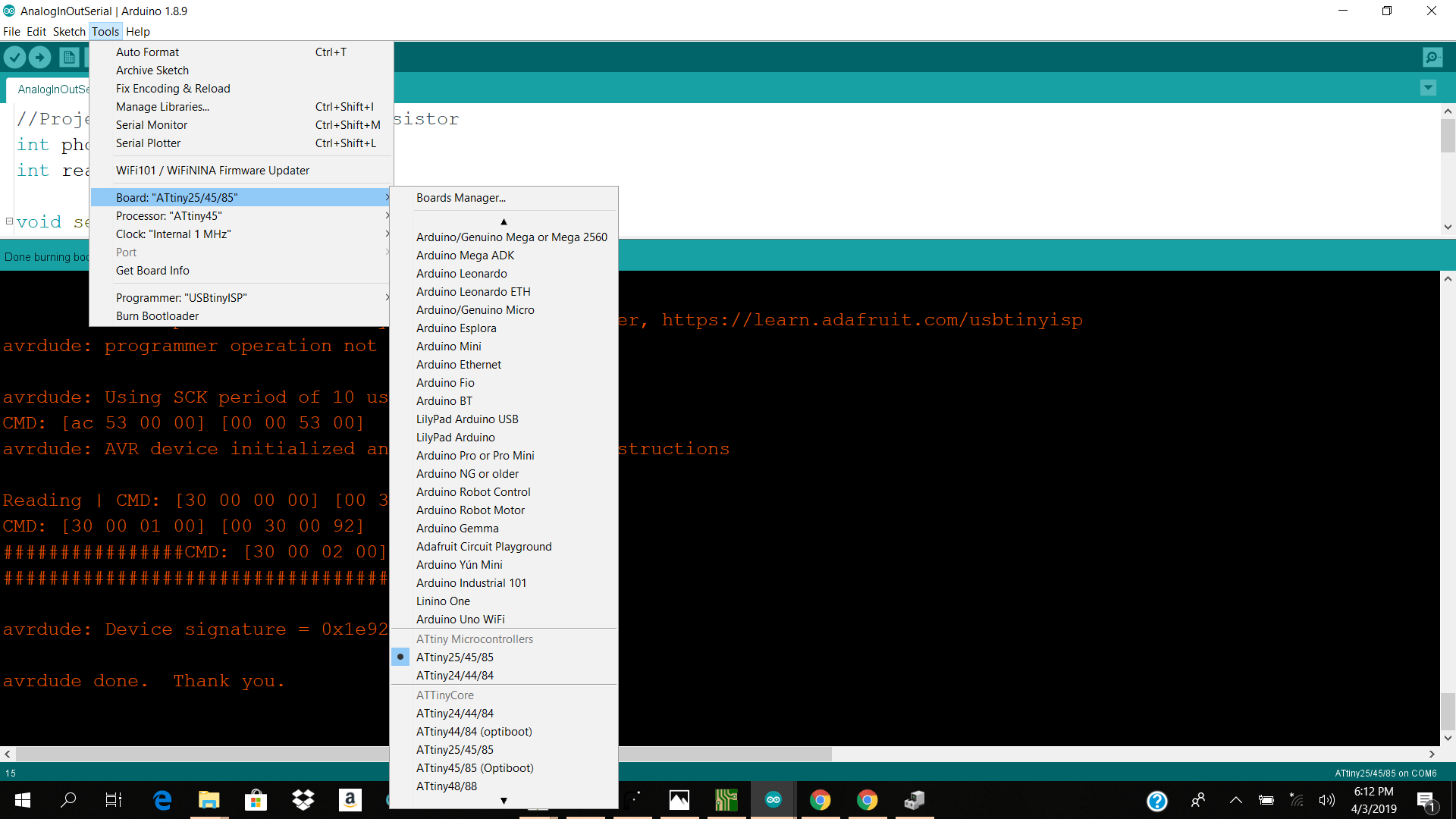
 I then went ahead and wrote a program to read from my phototransistor and send the reading over serial. So this took me a while. I had to do a few tests until I realized that I needed to swap my rx with my tx in my code then it started to work . So alittle about my code
I started off by importing the software serial library to speak to my attiny hardware serial. I then defined my rx and tx pin (reverse the pin num rx goes to tx n tx to rx).
I defined my Analog input pin that the phototransistor is attached to which was 2
I called softwareserial myserial you can give it your own name. I then made rx pin an input pin and tx an output pin and started the serial on baudrate 2400 waited for 5 seconds then started the loop.
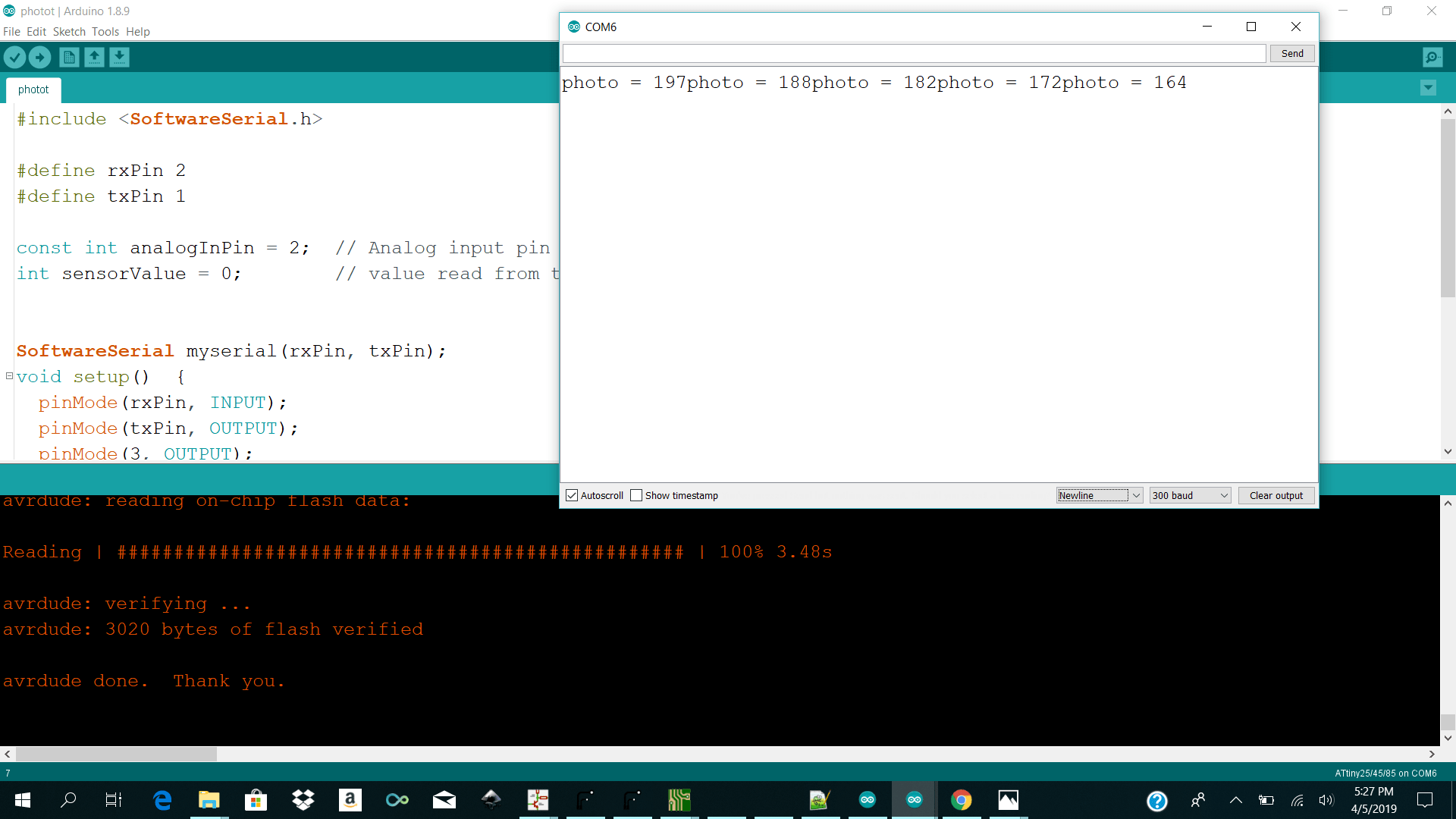
In the loop I read from the Phototransistor and send it over serial and write it to serial monitor. As you can see it worked!
I had to disconnect my fab isp and connect my ftdi cable to my pc it showed up on Com6 and open serial monitor on arduino ide and saw my reading.
One strange thing which happened which I havnt figured out yet was why when I program my serial to start at baudrate 2400 and open baudrate 2400 on arduino ide it did not work only when I open baudrate 300 on arduino ide it worked.
I then went ahead and wrote a program to read from my phototransistor and send the reading over serial. So this took me a while. I had to do a few tests until I realized that I needed to swap my rx with my tx in my code then it started to work . So alittle about my code
I started off by importing the software serial library to speak to my attiny hardware serial. I then defined my rx and tx pin (reverse the pin num rx goes to tx n tx to rx).
I defined my Analog input pin that the phototransistor is attached to which was 2
I called softwareserial myserial you can give it your own name. I then made rx pin an input pin and tx an output pin and started the serial on baudrate 2400 waited for 5 seconds then started the loop.
In the loop I read from the Phototransistor and send it over serial and write it to serial monitor. As you can see it worked!
I had to disconnect my fab isp and connect my ftdi cable to my pc it showed up on Com6 and open serial monitor on arduino ide and saw my reading.
One strange thing which happened which I havnt figured out yet was why when I program my serial to start at baudrate 2400 and open baudrate 2400 on arduino ide it did not work only when I open baudrate 300 on arduino ide it worked.
 The next step for me to do is to program my dht sensor I have tried a few examples but I still have not goten it to work because when I tried to use my dht and phototransistor together on my attiny 45 I get a message which says memory is my memory is almost full. I am persuming that I do not have enough flash memory for my code.
I am still working on that.
I am concluding that I did get my phototransistor analog sensor to work only the digital dht to go.
The next step for me to do is to program my dht sensor I have tried a few examples but I still have not goten it to work because when I tried to use my dht and phototransistor together on my attiny 45 I get a message which says memory is my memory is almost full. I am persuming that I do not have enough flash memory for my code.
I am still working on that.
I am concluding that I did get my phototransistor analog sensor to work only the digital dht to go.
Download Links Here
Kicad Sketch Zip
Kicad Gerber Files
input-nc files / front and edge cut
Phototransistor Arduino Ide Code
Contact Us
Where To Find Us
Paramaribo Suriname
Ethnalaan
50..