“When Moore’s Law (everything digital gets faster, cheaper , and smaller at an exponential rate) and Technology joined together, an explosive force was unleashed that changed the very nature of innovation, relocating ir from the center (governments and big companies) to the edges (a twenty-three-year-old punk rock musician and circuit-board geek living in Osaka, Japan).” - Joi Ito
Electronics Design
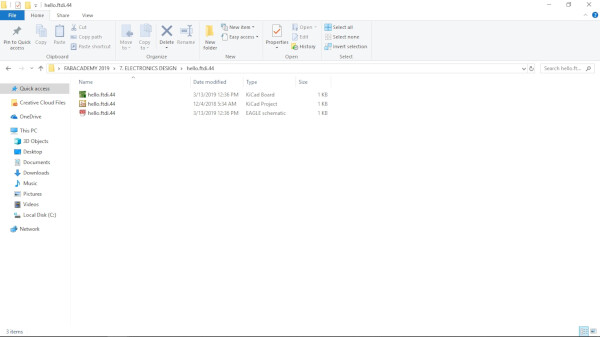
This week I'll first replicate the design of the hello.ftdi.44 board and then remix it to add some extra components. For this assignment I'm planning to use kiCAD to do the electronic design, as is opensource and I want to explore it. I have used Eagle before, so if everything fails with kiCAD, I'll use to make the design.
KiCAD
First I created a new project File > New > Project.
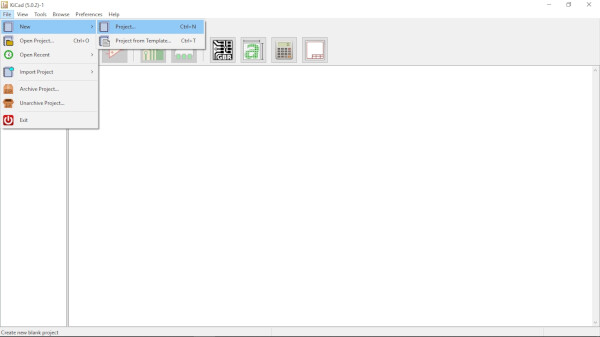
This will create a folder, where you select, which contains:
- KiCAD board file
- KiCAD project file
- KiCAD schematic file
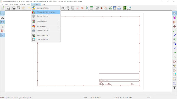
I found this FabAcademy documentation by Emanuele Goldoni that shows how to import the Fab library.
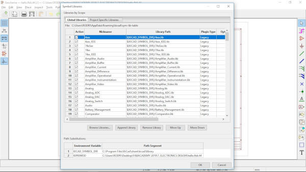
- Open Eeschema, the schematic layout editor, the first big button (As Emanuele sayed).
- Preferences > Manage Symbol Libraries
- Browse Libraries, select the fab lib file on your computer.
- Click OK
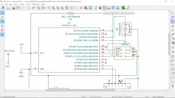
I started using the function in the third symbol on the right (that's the symbol of an OpAmp!), that let's you place components or symbols on your workspace. When you select where you want to place the component, it opens a window. I always typed "fab" to see all the components of the fab library.
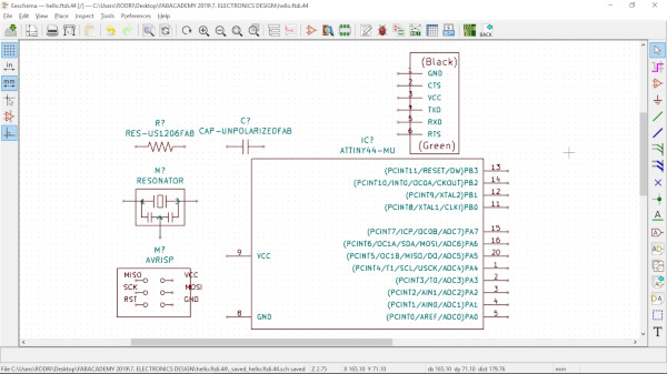
After droping some components I found that there's three versions of the ATTiny44 available:
- ATTINY44-MU
- ATTINY44-SSU
- ATTINY44-PU
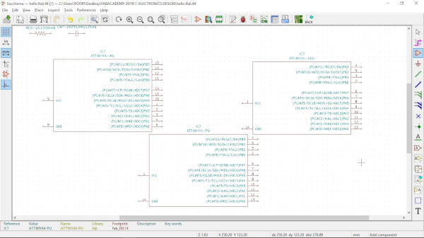
I noticed that the SSU and the PU had the same pinout arrengement, but the MU version was diferent. I chose to use the ATTINY44-MU as it has the same pinout as the one Emanuele used on his documentation.
Also I was a little bit confused about the crystal, because the one that appeared on my library only had two pins. I found that the component RESONATOR was the one used in the tutorial, and it has three pins as the hello.ftdi.44 board I'm replicating, so I'll use that instead of the crystal.
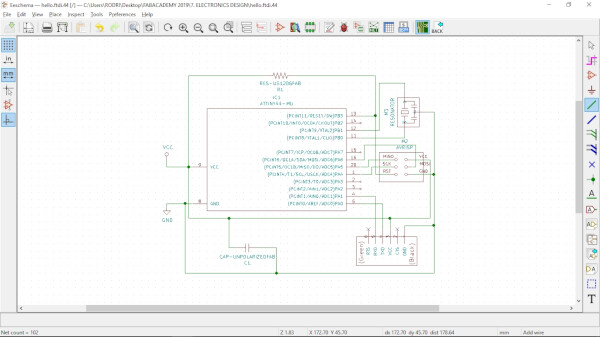
After droping all the components on the worktable I used the Place Wire (fifth symbol on the right) to connect the components.
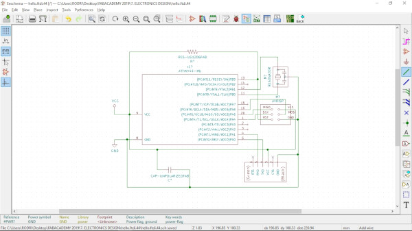
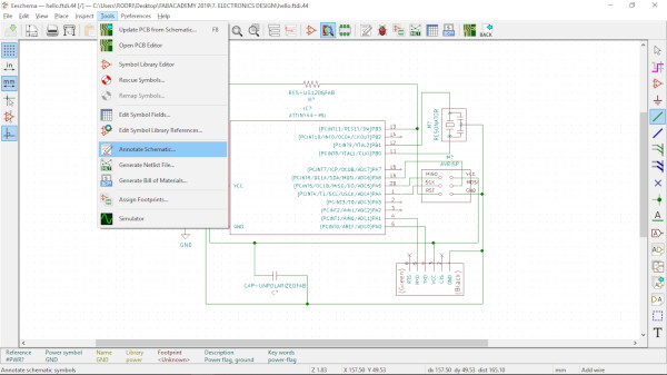
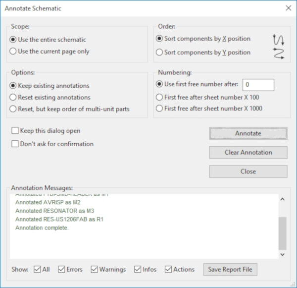
After doing that, I used the function Annotate Schematic to automatically number the different components over the schematic. Before doing that the components would show something like M?, R?, and after running the function it showed M1, R1, R2. So if you have different resistors, capacitors or any other component, you can now have a number asigned to each one.
- Tools > Annotate Schematic
- Click on the Annotate button.
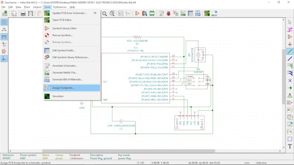
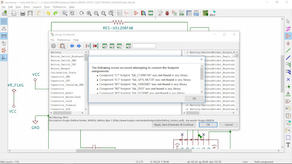
I ran the function Assign Footprints located:
- Tools > Assign Footprints
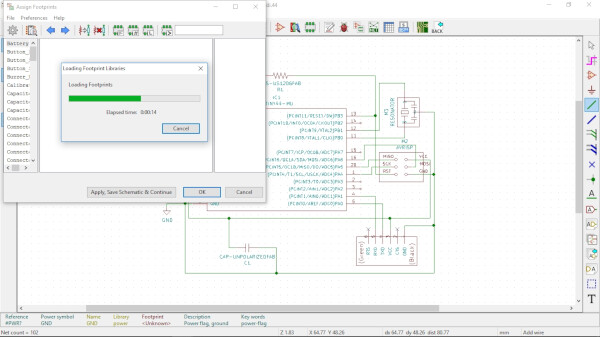
- A window opened and waited until the bar completely finished (it took aroun 1 min 25 seconds).
- Clicked Yes on the Confirmation window
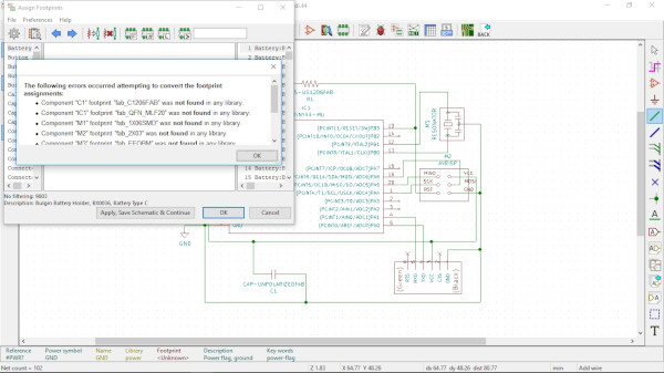
- A message of error appeared, showing that there was a few errors attempting to convert the footprint and I'll have to do it manually. I clicked OK
- Clicked Apply, Save Schematic & Continue
- Clicked OK
- IGNORING THAT MESSAGE WAS A TERRIBLE MISTAKE that I fixed later in the documentation.
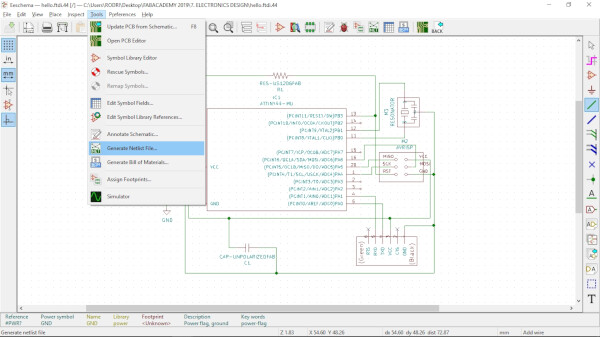
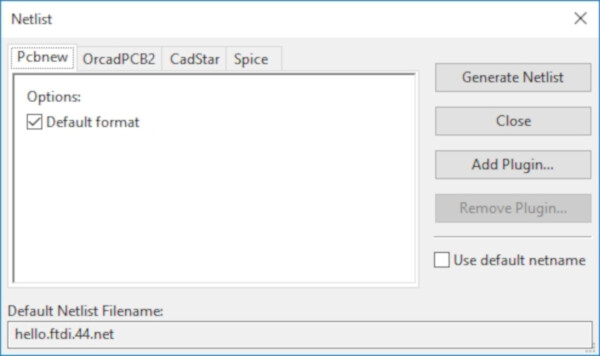
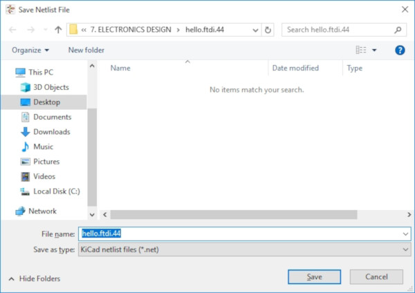
Then to Generate the Netlist File:
- Tools > Generate Netlist File
- Clicked on Generate Netlist button.
- Save file.
Click on the green circuit button at the top of the window (Run Pcbnew to layout printed circuit board). A new window opened
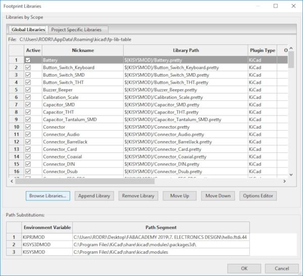
On the tutorial of Emanuele, he showed and improved version of the FabAcademy Library, so I'll use his file. I followed this instructions for the footprint Libraries for the PCB:
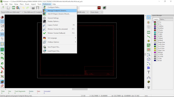
- Preferences > Manage Footprint Libraries
- On the open window, click on Browse Libraries.
- Select the folder of "fab.pretty". You can download it here or at the end of the page. LINK FILE!
- Click OK.
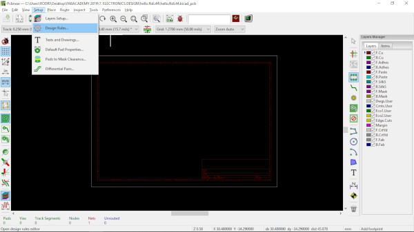
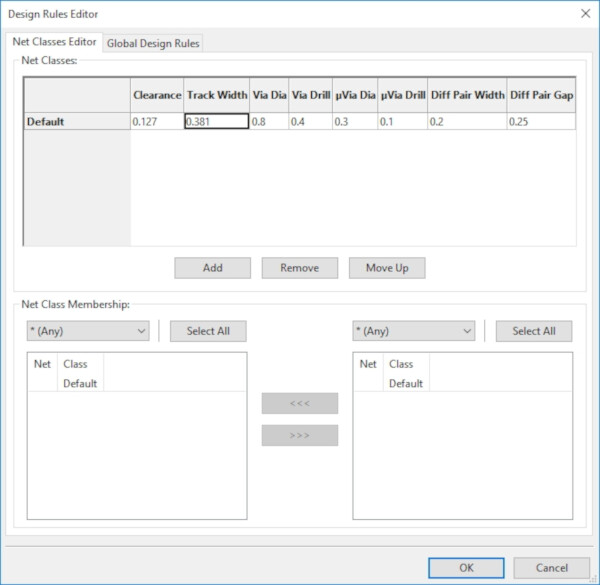
Setting the design rules:
- Setup > Design Rules
- Clearance: 0.127 mm = 5 mils
- Track Width: 0.381 mm = 15 mils
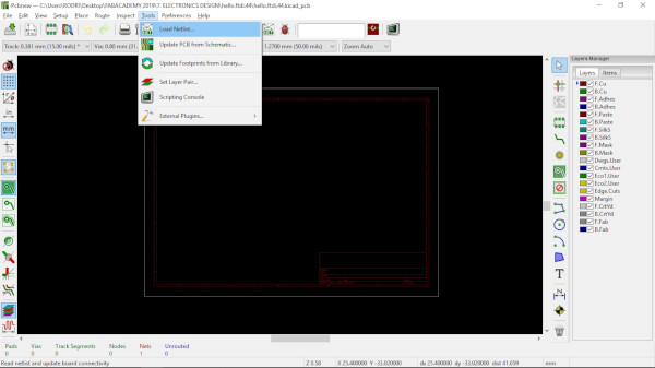
To place the components on the workspace:
- Tools > Load Netlist...
- The Netlist file I created was already linked in the window, so I clicked Read Current Netlist.
- Multiple errors showed on the window. I closed the window.
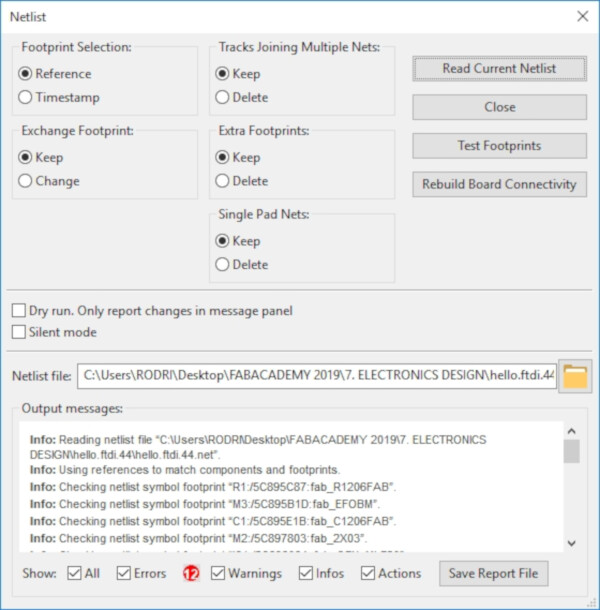
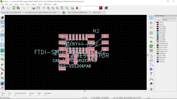
I don't know if anything changed with I just did. I clicked on the workspace and a window Choose Footprint appeared. I typed "fab" to see if anything came out. There's a few components but I didn't find the ATTiny44, so I'm thinking something went wrong when I first tried to import the footprints and the netlist.
I came back to the schematic, and selected:
- Inspect > Electrical Rules Checker
- Select Run
This showed a lot of places where there was no connection. So I redraw them to see if then I can generate properly the Netlist File. Almost every connection problem was resolved by doing this, except the power ones (VCC and GND) which I found pretty strange. So I read the Getting Started with KiCAD file linked in the FabAcademy archive, that thankfully has a section explaining this (page 18).
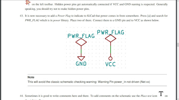
I inserted other pair of VCC and GND symbols and connected them to Power Flags. Still the Electrical Rules Checker gave me errors. After a few hours trying to solve this, rearrenging the wires, deleting and reinserting components and moving the VCC and GND components, still didn't work, but I don't think it has to do with the software not finding the components when I clicked on Load Netlist, so I returned a few steps back and I'm going to ignore that for a while and try to solve the missing components problem.
Researching the problem on Google ("kicad missing components"), I reached this video about CvPcb, that is a tool to link the schematic symbols to the PCB footprints. The forums I checked refered to this step to solution the missing components problem.
In the schematic, there is a button on the upper bar that says "Assign PCB footprints to schematic symbols". I clicked and a new window opened. This window looks familiar... It was the same one I ignored a few steps back and caused all of this trouble!
So from the list of missing components that is showing in the window, I selected the component and assigned to one of the right column. I'm selecting the ones of the fab.pretty librarie to see if it works.
To see how the components footprints looks like, I clicked on the second button on the upper bar (View selected footprint).
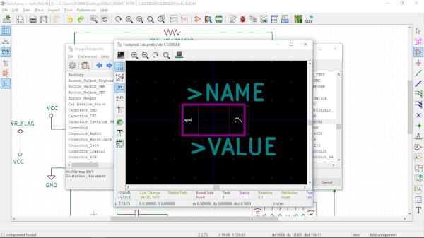
When assigning a component to the ATTiny, I noticed that the shape was a square with pads in every side, and that's not how the real component looks like. So it was possible that I selected a wrong type of ATTiny44. Researching a little bit, the SMD components that we have physicaly, with the pads on the sides, appear as SOIC components, so I have to switch the component ATTINY44-MU (square shape) to the ATTINY44-SSU (the right one with the pads to the sides). Doing this means I'll have to reconnect the wires.
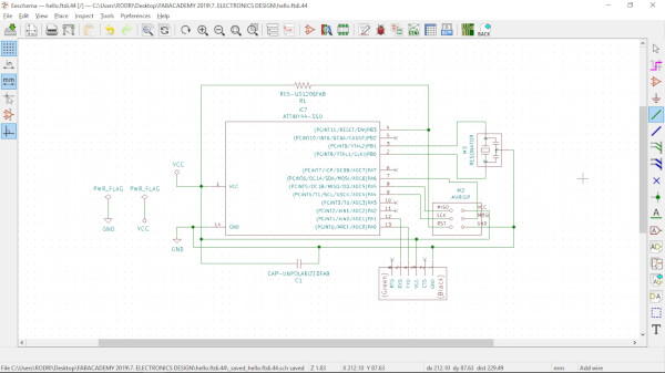
After finishing reconnecting I had to run Tools > Annotate Schematic again to assign a nomber to the new ATTiny component.
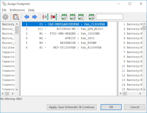
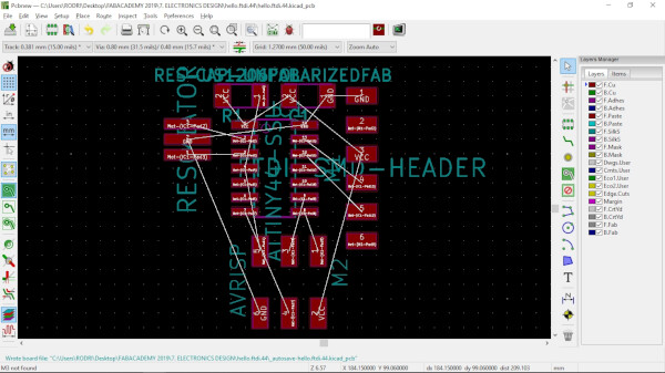
Then, clicked the button to convert Schematic symbols into PCB footprints, and select one by one the components that aren't recongized. Here's a list of the assigned components:
- C1 - CAP-UNPOLARIZEDFAB : fab_C1206FAB > fab.pretty:fab-C1206FAB
- IC1 - ATTINY44-SSU : fab_SOIC14 > fab.pretty:fab-SOIC14
- M1 - FTDI-SMD-HEADER : fab_1X06SMD > fab.pretty:fab-1X06SMD
- M2 - AVRISP : fab_2X03 > fab.pretty:fab-2X03SMD
- M3 - RESONATOR : fab_EFOBM > fab.pretty:fab-EFOBM
- R1 - RES-US1206FAB : fab_R1206FAB > fab.pretty:fab-R1206FAB
After doing this I generated the Netlist again. Then in the Pcbnew window I loaded the Netlist.
It finally worked!
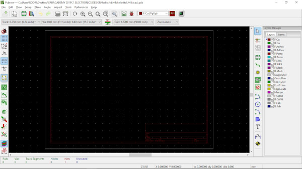
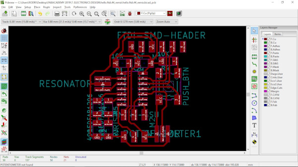
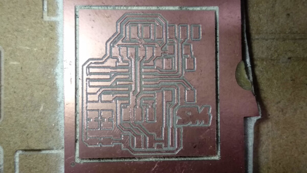
I rearrange the components to look like the reference board.
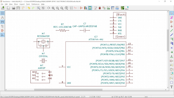
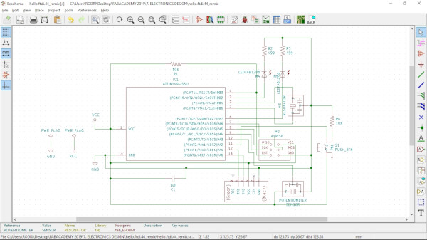
Now the fun part is to add some new components into the existing board, and then fabricate it. For that I used this image and this reference to connect the components in the available pins of the ATTiny44.
Repeating the same process as before:
- Place new components.
- Wire them to the respective ATTiny44 pins, GND and VCC.
- Run Tools > Annotate Schematic
- Run Tools > Assign Footprints, select the respective ones.
- Run Tools > Generate Netlist File
- Open the PCB Editor
- Run Tools > Load Netlist. Select
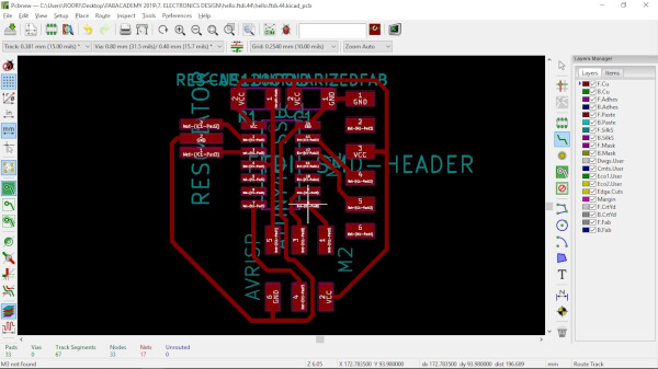
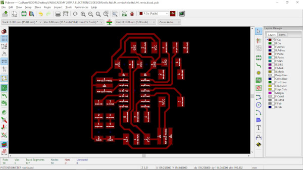
I rearrenged the components. The most difficult part this time was to connect the VCC and GND of the new added components. My workflow was order the same components as the original board first. Then added the new components were I think they're going to be better. I had to draw and erase the tracks many times figuring out the best way to connect them. At then end I had this:
After this I wanted to give the board an interesting shape of the profile. I did this:
- Export the board as a SVG
Drawing the outline
To do this I used Inkscape. First I opened the SGV into Inkscape.
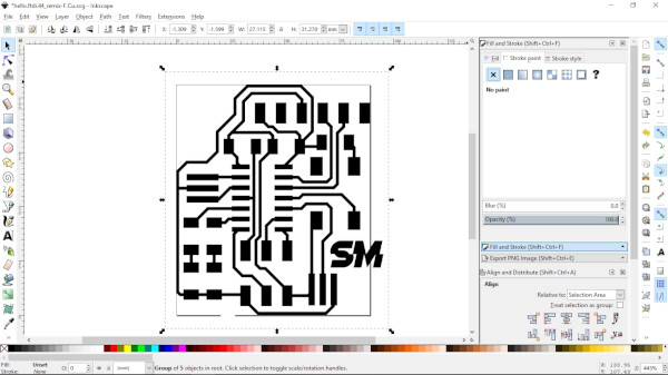
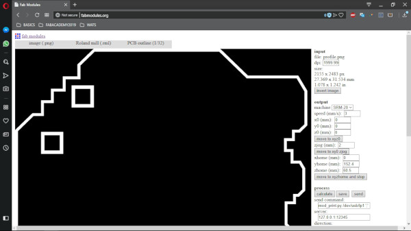
I added a symbol SM (for SpaceMonkey) and draw the outline using the bezier tool.
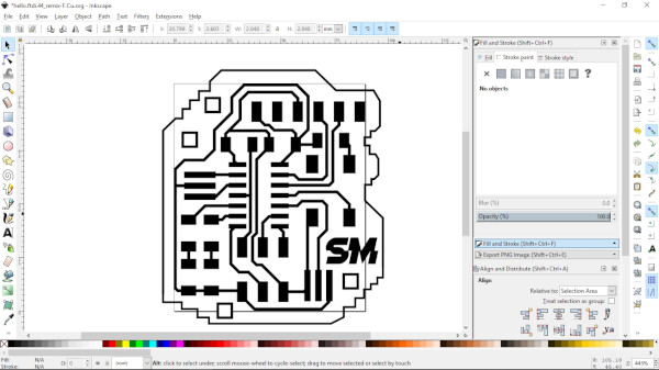
I exported the traces and the profile as separated png files, with 2000 dpi.
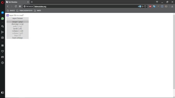
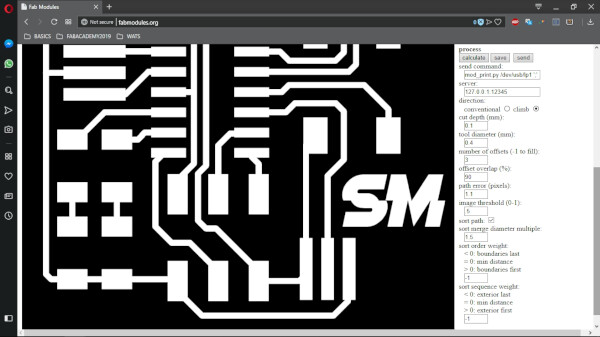
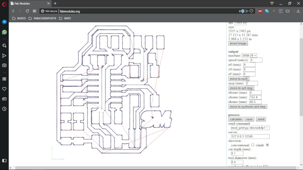
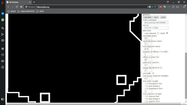
FabModules
To fabricate the board I used FabModules.
I generated the .rml file for the Roland SRM-20. First I did the traces file.
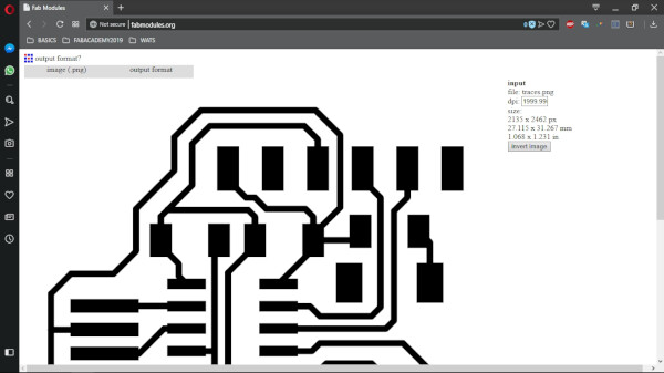
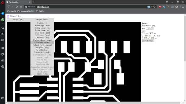
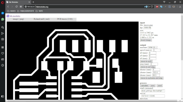
Then I generated the profile file.
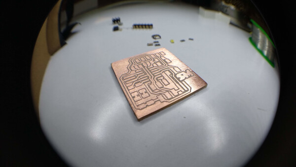
Fabricating the board
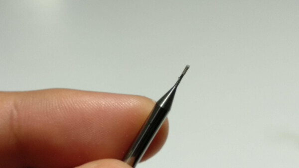
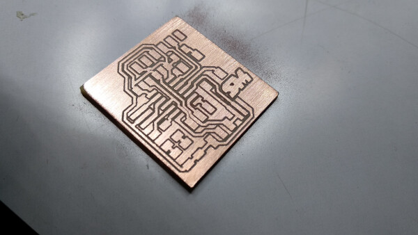
I used the Roland SRM-20 that we have in the lab to mill the board. I used a 1/64" mill bit for the traces and a 1/32" mill bit for the profile of the board.
To control the Roland, I used VPanel.
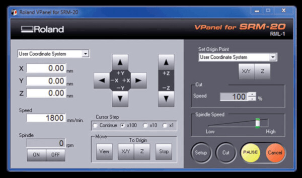
The milling of the traces went okay, but at the profile cut it completely destroyed the board. After analising what the FabModules did with the profile, it seems that the shape generated an offset.
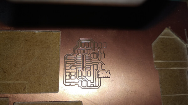
I generated a simpler profile, just a plain rectangle.
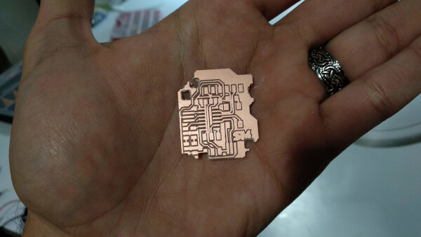
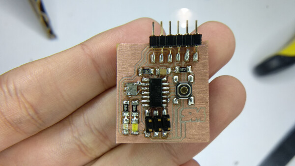
I then soldered all the components to the board.
As you can see in the video, I has trouble soldering the resonator (the last component), so what I did was soldering the three pads, and then heating the component with the iron tip until the solder joints.
Files
- Hello board traces .png
- Hello board profile .png
- Hello board Schematic .sch (KiCAD)
- Hello board PCB .kicad_pcb (KiCAD)
- Hello board KiCAD Project .pro (KiCAD)