7. Electronics design
February 20
Assignments
group assignment: group project: use the test equipment in your lab to observe the operation of a microcontroller circuit board.
individual project: redraw the echo hello-world board, add (at least) a button and LED (with current-limiting resistor) check the design rules, make it, and test it extra credit: simulate the operation.
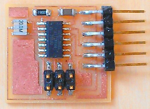
Hope to get sommething close to this:
individual assignment (under
Summary
We have tested the microcontroller circuit in operation using the oscilloscope and the multimeter.
Doing online zapping I found out that the ATmega328 or ATtiny44, are simple to hack: see article of Sergei P. Skorobogatov, bottom of the page, https://www.cl.cam.ac.uk/~sps32/mcu_lock.html.
I also scroll a lecture about how chips work, and what is inside, by Ken Sirriff at the 2016 Hackaday SuperConference.
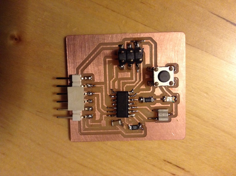
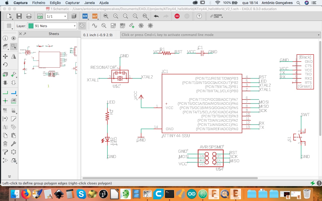
The I get into EAGLE and start to built a step by step intro to it. The steps are listed bellow. The result was this one:
Todo
- Just for fun, the Zeptobars blog shows pic inside an ATmega8, an ATtiny13A, or a ATtiny4.
- What’s inside an IC? Ken Sirriff lecture here, at the 2016 Hackaday SuperConference
- What’s inside an IC, part II? Getting insine your inner chip
- Issue about EAGLE Fab.lbr
- Voltage measuring
- Arduino pins that oscilate (float): put vimeo video!?
- Circuits Simulation
Work done
The work group was done after the individual was accomplished.
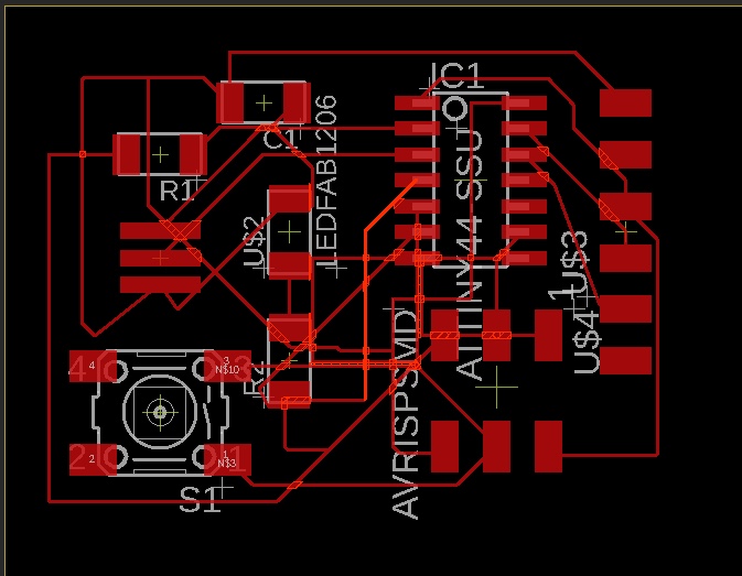
In this individual work, I want to add to the PCB we are suppose to built, a water sensor and a led. The idea is this to be used as security sensor at my boat project, that is, if the hull is flooded a CO2 solenoid valve acts to inflate a balloon.
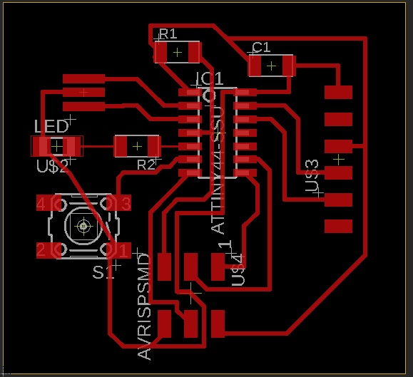
So, i’m going to use EAGLE to make this PCB sketch:

I reviewed the week 7 lecture in order to plan the week work.
What’s inside an IC? By Ken Sirriff lecture here, at the 2016 Hackaday SuperConference
Time line description of the former video in order to have a better mental model of a processor:
- 5:10 video, ALU
- 5:58, MOS transistors
- 6:40, MOS transistors sensitive to electrostatics explained
- 7:10, PIOS, why to not use that word?
- 7:16, NAND gate
- 8:25, PULLUP resistor, is what?
- 9:01, NOR gate
- 9:48, a single gate his five!
- 10:57, Sinclair Scientific calculator, 1974
- 12:15, Simulator calculator, http://www.righto.com/2013/08/reverse-engineering-and-simulating.html
- 14:01, Intel memory, 1970: 512 bits, half a tweet
- 15:08, wait for the bit, sequential
- 15:46, 555 timer
- 16:00, bypolar transistors theoretically and real!
- 16:45, real NPN transistor
- 17:20, real PNP transistor
- 17:53, 555 timer, or read it here; for the CMOS version of it, here
- 18:44, simulation here
- 18:57, 741 opamp
- 20:37, current mirror
- 21:18, resistors are to “expensive” inside a chip
- 21:30, Bizzards to “clone” currents
- 22:12, 7805 voltage regulator
- 24:31, how to photograph this?
- 26:02, How to get to the die?
- 26:36, die photos: here, here and here
- 27:24, chisel
- 28:12, Intel 8008
- 29:10, thank you very much
Material list
| Electronic Parts | Characteristics | Notes |
|---|---|---|
| ATtiny44 | ||
| LED | ||
| Wires | two | water sensor |
| ISP | 6 pins | Header for in circuit programing |
| Capacitor | 1 microF | Filter capacitor |
| Resistors | 0.5K | Voltage divider to protect the LED |
| Resistors | 10K | PullUp for reset |
| Ressonator | 20 MHz | No need, just for the processor to be faster |
| FTDI []^1 | 6 pins | Header to USB connections |
| Switch OMRON | 6MM_SWITCH | Connect to I/O port B or A, all have internal pull-up resistors |
| UV index sensor |
[]^1
Step 1: design it
I started to watch Eagle tutorials to get started with the basic steps.
In the middle I run into ATtiny44 datasheet and looking into the pins functions, I found this image of former Fab Academy Student, 2018, Aby Michael:

Then I follow this steps:
- Open a NEW project, on the menu or at the control pannel: go to “file”->”new” and click on “E project”, I called ” ATtiny44_fab2019_antonio”: all the files will stay in the same directory; OR, in your left pannel, click on Projects to open projects directory and right click on the folder projects to create a NEW one;
- (optional) Verify your folder project directory: go to “options” and click on “directories”;
- (optional) verify that your project name has a green dot, saying its your open project;
- right click on the project name and choose New schematic;
- If you need to install a library: save your library file with the extension .lbr, like fab.lbr, in your computer folder;
Fab Academy 2019 availabe library here
- Click on the menu: file -> new -> library
- Click on the left up button open;
- Browse your .lbr file;
Don’t forget to, in the library manager window to press use;
- Click on the save button, to save the library you choose.
- more here
- (optional) What libraries are available? Awnser here;
- (Optional) Installing new lybraries: learn here
NOTE: important concepts: device, footprint, 3D packege and symbol;
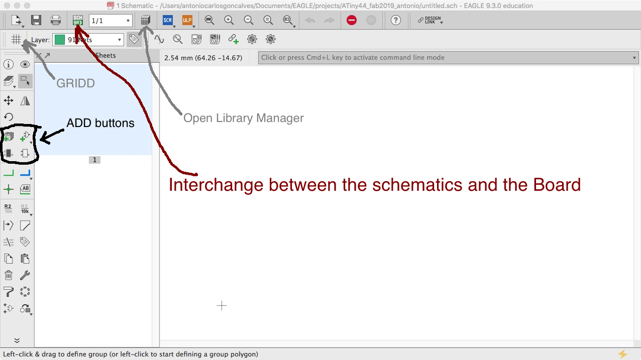
- You can see the board if you, at the schematic file of your project, click on the icon Generate/switch to board, just in the left, bellow the menu.
NOTE: if the down left corner button is GREEN, your board is connected to the schematic in real time. Meaning, if you change one of the files, they will change to.
Very important Basic Commands for the beginner: 1:30 of this video
- (Optional) schematic learning here
Eagle menu
-
look at the you material list (up on this screen) and Add components: really complicated! (Eagle Tutorial)
-
(optional) If your library doesn’t showed, open library manager; browse the library you want and click on use.
-
(optional) For other unity, click on GRID and select the one you want;
-
Define connections
-
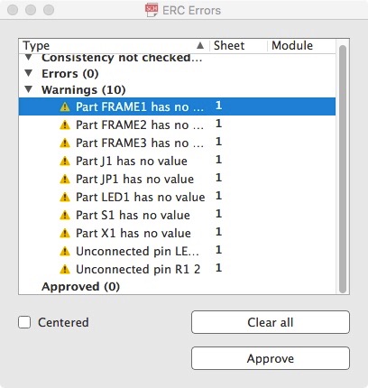
Run ERC to find errors if EAGLE can’t generate the board;
My first board errors
- (if too many errors) Restart: sorry! ;)
(my first) so wrong!
- (second attempt) At this type, my tutor, Filipe, tells me to go another away: label every pin and follow exactly the design proposed To learn how to labell using EAGLE just follow this video at 2:50.
-
Switch to board by clicking on the tool switch between BRD/SCH (see the picture above: step 14);
-
Make the routes: automatically or by hand: trial and error.
Very HARD job!!!
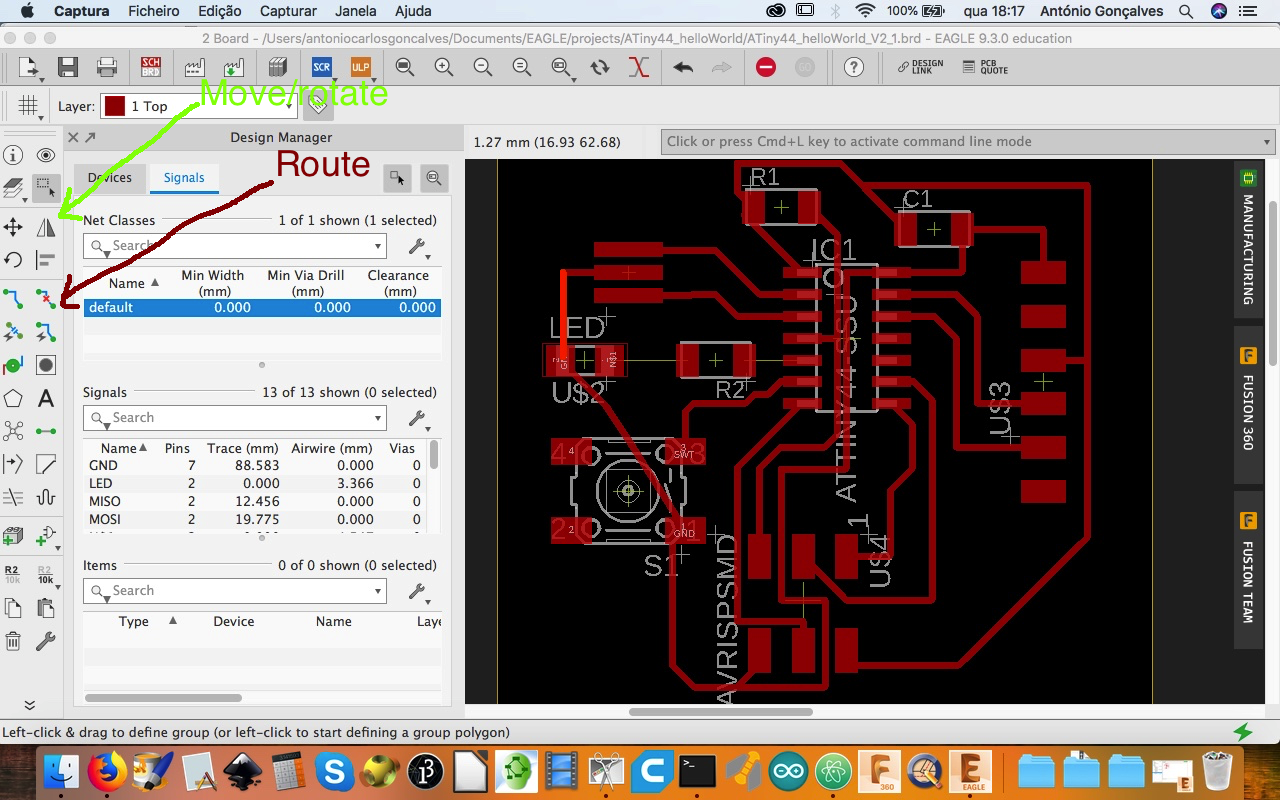
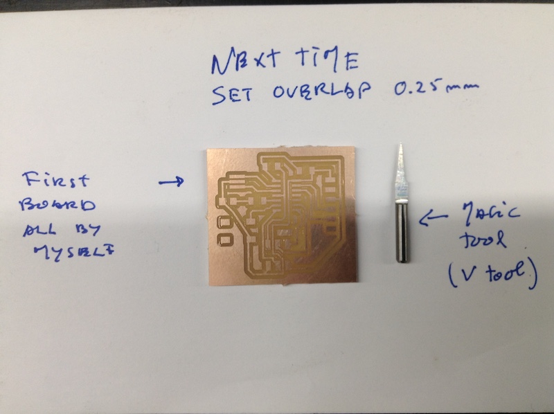
- After ajusting it, increasing the route width to 0.4 mm (choose your own width at the left menu, where you can find the “width”: click on it after you scroll all the way: step 1 here, the outcame:

Note
You need also to choose the space in between the routes, at least 0.3 mm: change it using the ALT button + drag the route with the left mouse button.
Step 2: make it
At this point press Manufacturing (the top icon with the factury form and the green arrow) to save the board in DXF: procedure of week 05: eletronics production.
The second try. The first one I forgot yo drqw same routes and perhaps the reference (0,0,0) was not correct:
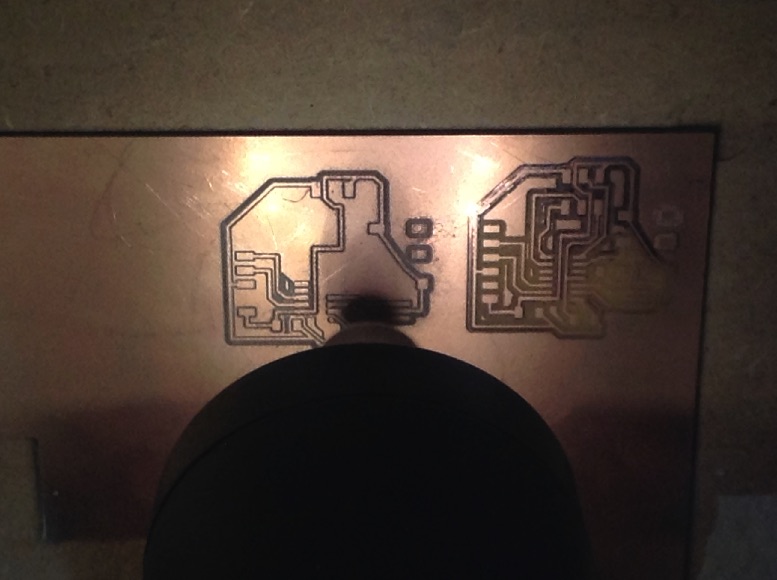
The third try. It seems better but some of the paths are two close. Let’s see in the testing.
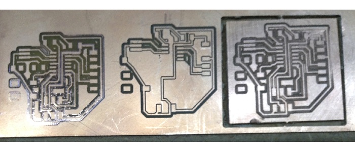
A closer look it looks nice:
Debugging.
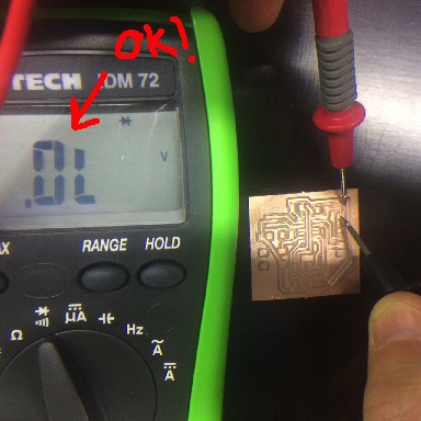
Testing the conductivity? OK!!! Not only the other paths are correct as well as the problematic ones, by hyphotesis, are correct. Very good. I’m starting to be confident in using the milling machine. I also tested the 5V pins with the multimeter.
Did I do sommething wrong? Catch the diferences!? (see step 24)
The third try: not bad!
Note
Same usefull tips: https://www.autodesk.com/products/eagle/blog/top-10-pcb-routing-tips-beginners/

Result
Step 3: test it
Use the Neil_Gershenfeld program to see if the board is working, this is available here.
To install averdude on Mac I follow this page Install avrdude on Mac OSX
Test it with IDE Arduino… done!
Test it with C programing… not yet!
Step 4: simulate it
I will try to use the Proteus like Jose Fuenzalida did here at 3D Experience Lab, Boston.
Work group
We measure the frequency and the change in a pin floating. We found for the frequency:
Wave time Period (T) 2 x 10^-6 s, which means a f = ½ x 10^-6 s = 50 KHz. The wave amplitude pk to pk, 100 mV or 296 mV.
(include pic about voltage measuring)
Measure voltages on the pins: I confirmed it, we found 5 V. Debugging was a major issue in order to get starting to program the board. We did define the same strategy as with the ISP:
- Found the 5 V
- Testing shorts and conductivity
- Remove small copper parts
- Clean ans washe the board: I did it twice:
Danger
Its not danger but my pcb didn’t make the serial connection to show at the serial monitor: it always showed an error. The error was quite simple: WRONG pin!
TX - pin 12 RX - pin 11