#Week 07 / Electronics Design
Step 1) Board Schematic and Layout design.
Step 1.1) KiCad
For PCB prototyping I chose KICAD, It’s free and also you can download all libraries for Digikey products. Also, it has a Schematic Capture, PCB Layout, and 3D Viewer.
Schematic Capture)
Schematic capture is efficient, with all the tools you can expect for such a task. The interface focuses on productivity. There are no complexity limits, as large designs can be divided into hierarchical subsheets. Various export options are available (PDF, SVG, HPGL, Postscript).
Electrical Rules Check)
The electrical rules check (ERC) automatically verifies your schematic connections. It checks for output pin conflicts, missing drivers and unconnected pins.
Exports netlists in formats such as)
Bill Of Materials)
BOM generation is extensible via Python scripts or XSLT, which allows many configurable formats.
Integrated libraries)
KiCad comes bundled with a vast library of symbols, footprints, and matching 3D models. They are community maintained so they never stop improving.
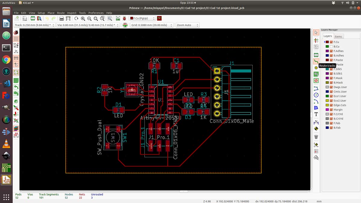
Push and shove router)
This modern tool will help you lay out your board faster. As you draw your track, it pushes forward traces that are in the way. If that is not possible, your track will be rerouted around obstacles. The push and shove router will make sure that your DRC constraints are respected.
Length tuning)
Tune trace lengths for high-speed designs with the dedicated tool.
3DViewer Features
When laying out your PCB, you can instantly inspect your design in an interactive 3D view. Rotate and pan around to inspect details easier than with a 2D display.
Step 1.2) Create a new project.
For a new project go to “File->New->Project” it will open the schematics window.
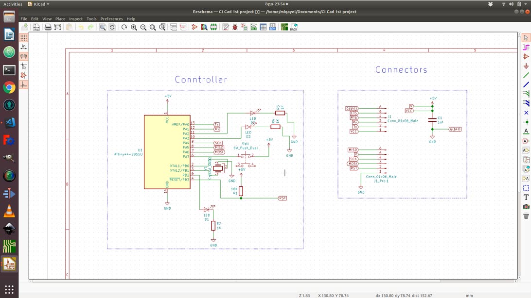
Step 1.3) Schematic .
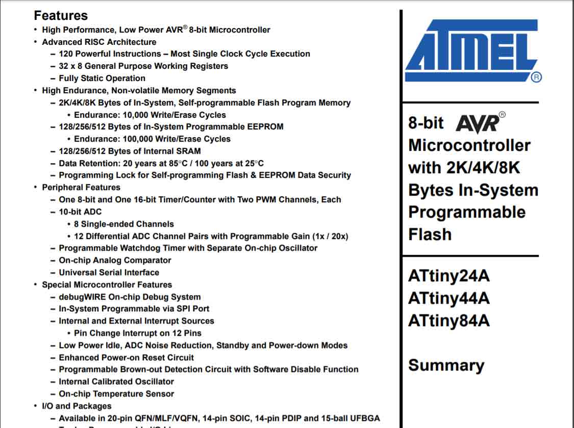
For schematics design at first, you need to understand what is the function of your board and decide which controller you must use for your project. In my case board must turn on the light whenever I push button or do some effects. The controller that I used is Attiny44A. Choosing the right controller is very important because the schematics start from the controller. Before starting sketching your board schematics you must look at your controller datasheet.
The important thing to look at in datasheet)
Features)
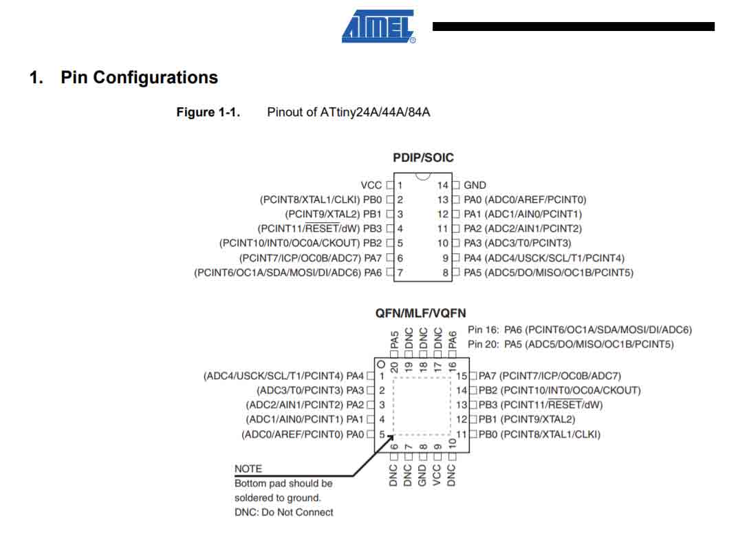
Pin Configurations)
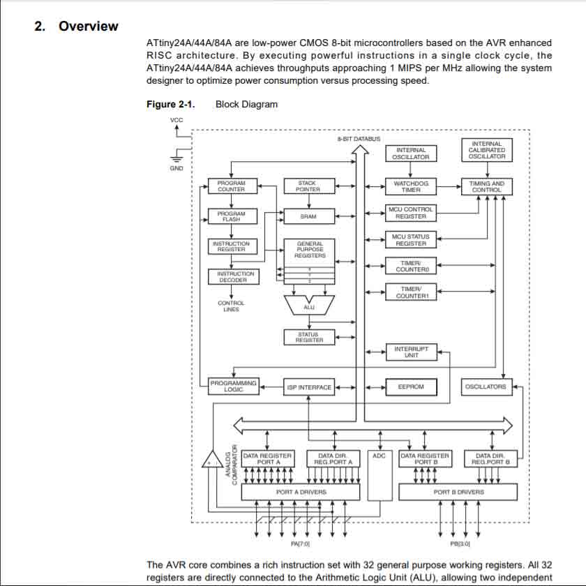
Block Diagram of the controller)
Here you can see all functional parts off your controller . For example, the ALU block is responsible for counting, GENERAL PURPOSE REGISTERS is for saving and sending the data.
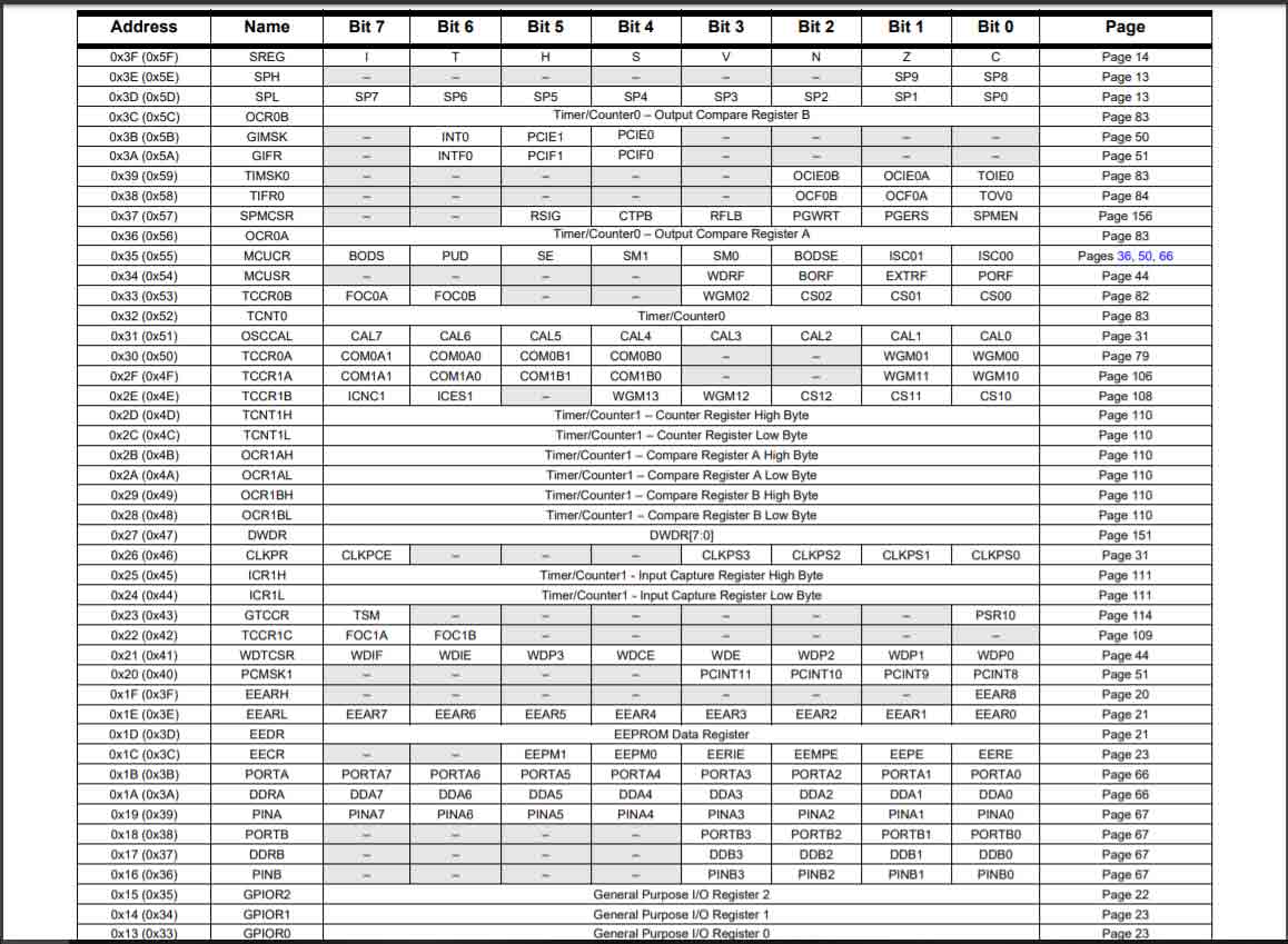
Register Summary)
Here you can see all register. The registers are for storing information and transferring it.
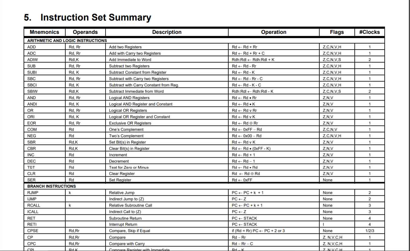
Instruction Set Summary)
This is the basic commands for programming you board in the low level of programming language such as assembler.
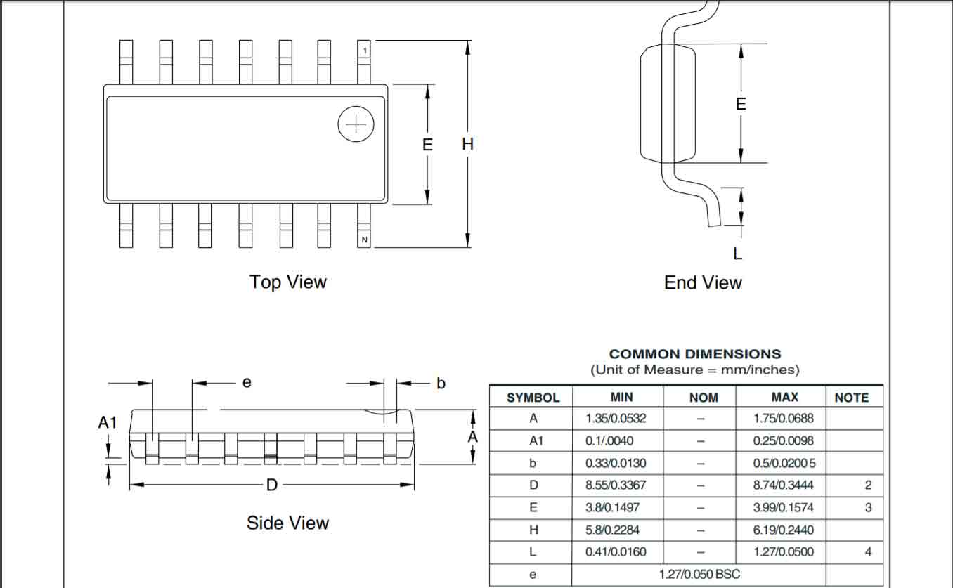
Packaging Information )
For our board we use 14S1 package size.
Step 1.4) The components.
You must choose the components with their footprint and value. You can name the pins, and by naming them you can connect them without lines. For my board I need
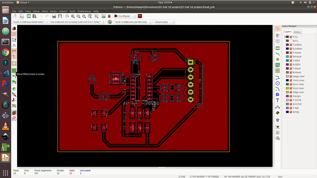
Step 1.5) Layout design.
For layout design, I used these tools.
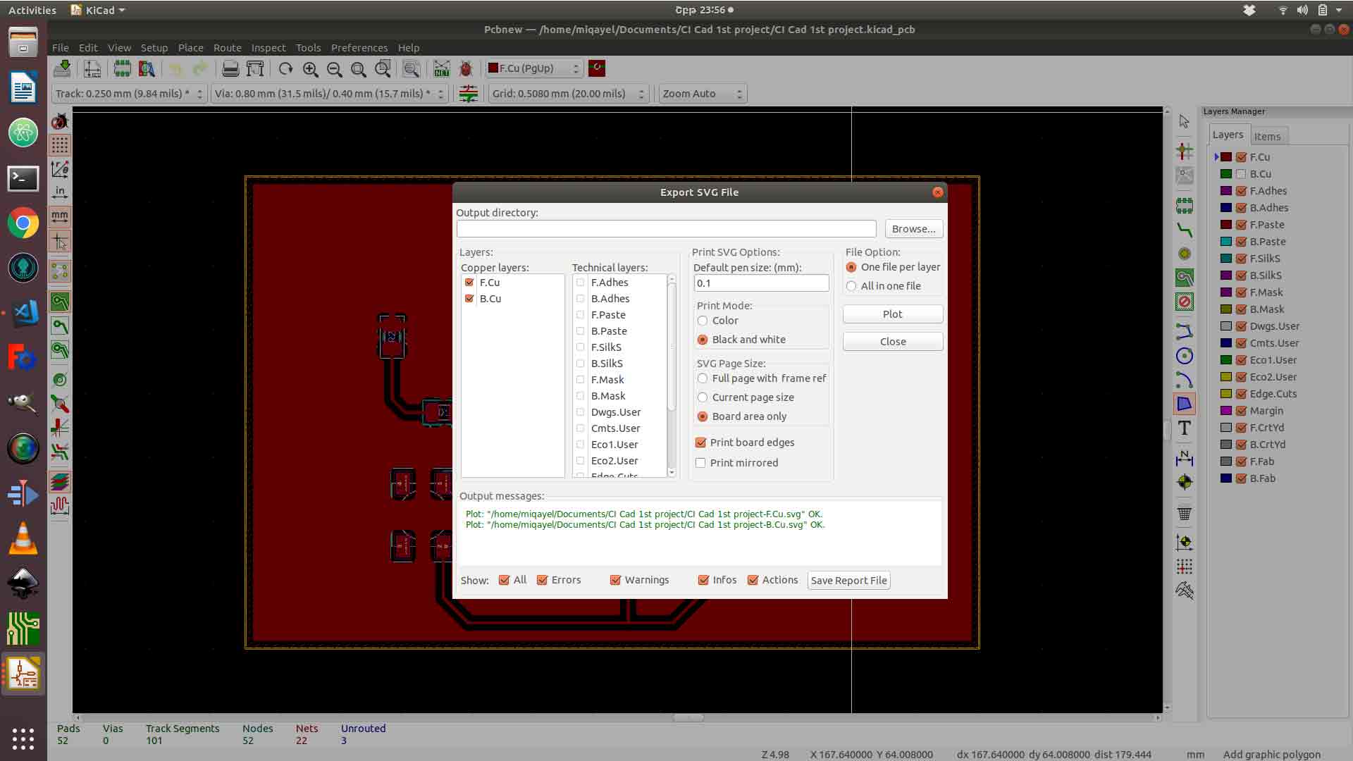
Step 1.6) Exporting
You can export your PCB layout in Gerber file format, but I exported it as SVG because “Fabmodules “ support SVG file format. Also, I make 3 images for my PCD manufacturing by using Inkscape.
Step 2) Setting up Fab Modules.
Step2.1) Upload image
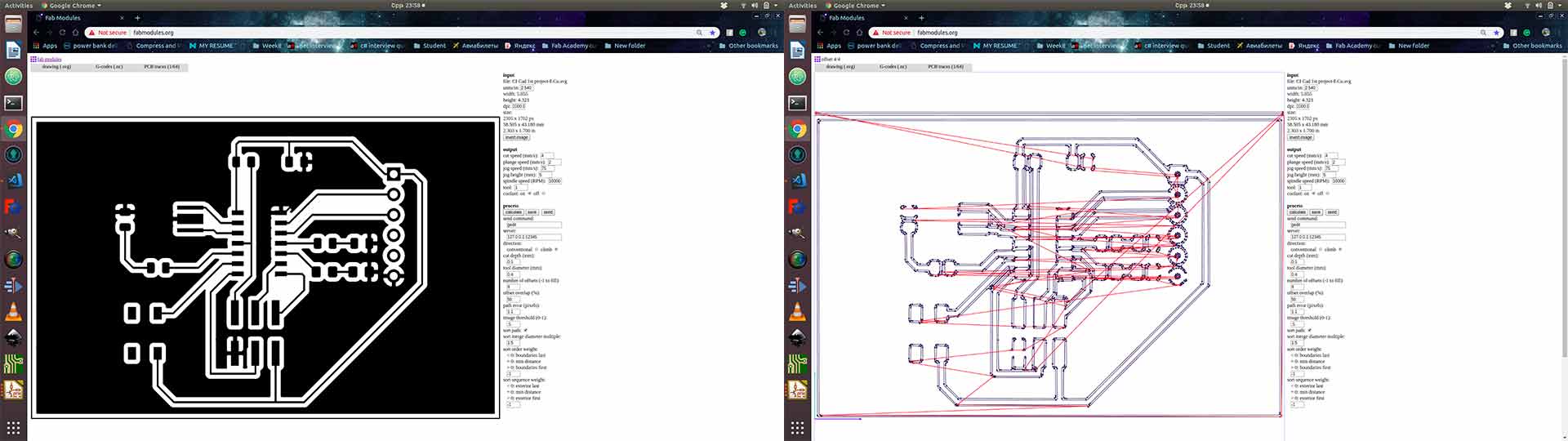
Step2.2) Choose output format (G code .nc)
Step2.3) Choose milling bit.
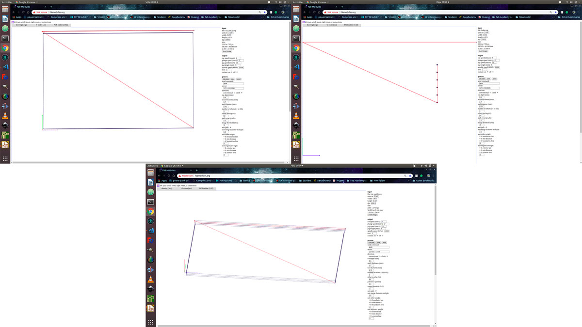
Sep 2.4) Calculate.
Step 2.5) Save.
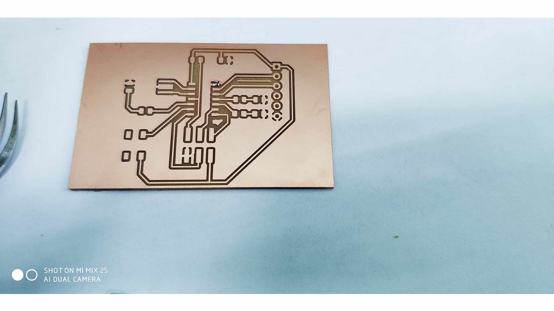
Step 3) PCB manufacturing.
The process of PCB manufacturing is described on week5.
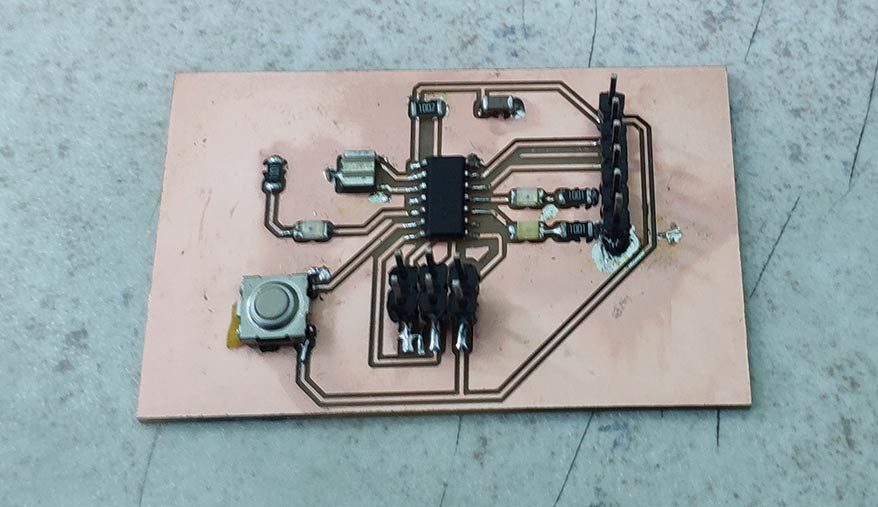
Step 4) Soldering.
The process of soldering is described on week5.