Electronics production
Introduction
Assignement for this week is• group assignment: characterize the design rules for your PCB production process
• individual assignment: make an in-circuit programmer by milling the PCB, program it, then optionally try other PCB processes.
During this week we will learn tecniques of making PCBs, soldering electronic components and programming them.
PCB (Printed circuit board)
Printed circuit boards are used in all but the simplest electronic products. PCBs can be single-sided (one copper layer), double-sided (two copper layers on both sides of one substrate layer), or multi-layer (outer and inner layers of copper, alternating with layers of substrate). Multi-layer PCBs allow for much higher component density, because circuit traces on the inner layers would otherwise take up surface space between components. The rise in popularity of multilayer PCBs with more than two, and especially with more than four, copper planes was concurrent with the adoption of surface mount technology. However, multilayer PCBs make repair, analysis, and field modification of circuits much more difficult and usually impractical. A basic PCB consists of a flat sheet of insulating material and a layer of copper foil, laminated to the substrate. Chemical etchingdivides the copper into separate conducting lines called tracks or circuit traces, pads for connections, vias to pass connections between layers of copper, and features such as solid conductive areas for electromagnetic shielding or other purposes. The tracks function as wires fixed in place, and are insulated from each other by air and the board substrate material. The surface of a PCB may have a coating that protects the copper from corrosion and reduces the chances of solder shorts between traces or undesired electrical contact with stray bare wires. For its function in helping to prevent solder shorts, the coating is called solder resist or solder mask. A printed circuit board can have multiple copper layers. A two-layer board has copper on both sides; multi layer boards sandwich additional copper layers between layers of insulating material. Conductors on different layers are connected with vias, which are copper-plated holes that function as electrical tunnels through the insulating substrate. Through-hole component leads sometimes also effectively function as vias. After two-layer PCBs, the next step up is usually four-layer. Often two layers are dedicated as power supply and ground planes, and the other two are used for signal wiring between components. "Through hole" components are mounted by their wire leads passing through the board and soldered to traces on the other side. "Surface mount" components are attached by their leads to copper traces on the same side of the board. A board may use both methods for mounting components. PCBs with only through-hole mounted components are now uncommon. Surface mounting is used for transistors, diodes, IC chips, resistors and capacitors. Through-hole mounting may be used for some large components such as electrolytic capacitors and connectors.
PCB design
• Schematic capture through an electronic design automation tool.• Card dimensions and template are decided based on required circuitry and case of the PCB.
• The positions of the components and heat sinks are determined.
• Layer stack of the PCB is decided, with one to tens of layers depending on complexity. Ground and power planes are decided. A power plane is the counterpart to a ground plane and behaves as an AC signal ground while providing DC power to the circuits mounted on the PCB. Signal interconnections are traced on signal planes. Signal planes can be on the outer as well as inner layers. For optimal electromagnetic interface performance high frequency signals are routed in internal layers between power or ground planes.
• Line impedance is determined using dielectric layer thickness, routing copper thickness and trace-width. Trace separation is also taken into account in case of differential signals. Microstrip, stripline or dual stripline can be used to route signals.
• Components are placed. Thermal considerations and geometry are taken into account. Vertical interconnect access and lands are marked.
• Signal traces are routed. Electronic design automation tools usually create clearances and connections in power and ground planes automatically.
• Gerber files are generated for manufacturing.
Copper patterning
The first step is to replicate the pattern in the fabricator's CAM system on a protective mask on the copper foil PCB layers. Subsequent etching removes the unwanted copper. (Alternatively, a conductive ink can be ink-jetted on a blank (non-conductive) board. This technique is also used in the manufacture of hybrid circuits.)First of all I took user manual of Srm-20 milling machine and started learning how operate it.
• Silk screen printing uses etch-resistant inks to create the protective mask.
• Photoengraving uses a photomask and developer to selectively remove a UV-sensitive photoresist coating and thus create a photoresist mask. Direct imaging techniques are sometimes used for high-resolution requirements. Experiments were made with thermal resist.
• PCB milling uses a two or three-axis mechanical milling system to mill away the copper foil from the substrate. A PCB milling machine (referred to as a 'PCB Prototyper') operates in a similar way to a plotter, receiving commands from the host software that control the position of the milling head in the x, y, and (if relevant) z axis.
• Laser resist ablation Spray black paint onto copper clad laminate, place into CNC laser plotter. The laser raster-scans the PCB and ablates (vaporizes) the paint where no resist is wanted.
•Laser etching The copper may be removed directly by a CNC laser. Like PCB milling above this is used mainly for prototyping. The method chosen depends on the number of boards to be produced and the required resolution. I will mill the PCB by Srm-20 machine.
 Fab ISP (In system programmer) is designed in fab lab and it is another version of an AVR programmer.
I should do the following actions:
• set up the machine for milling process
• prepare files for milling, I will use fab modules
• cut the board
• solder components
• programm the board
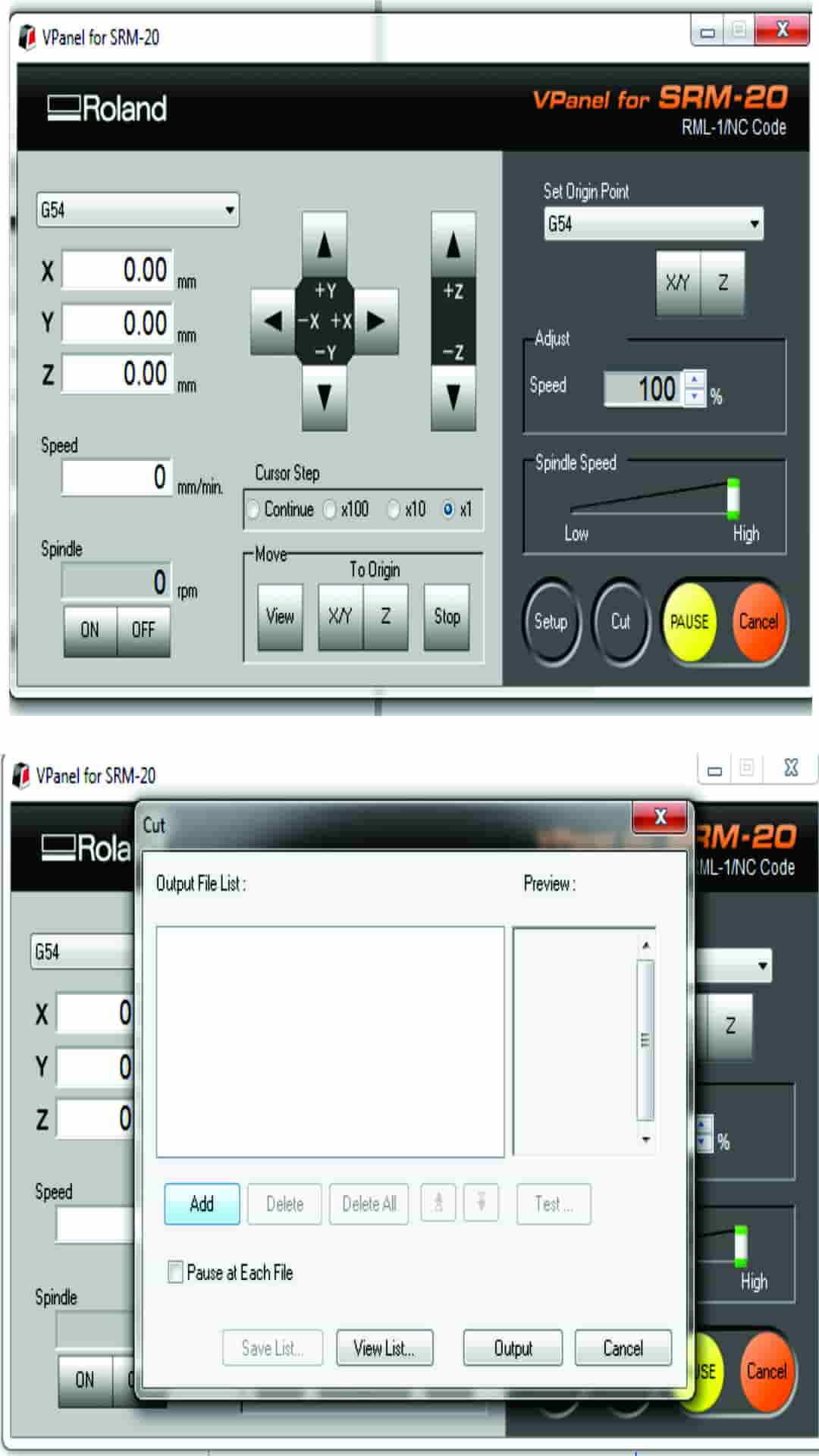
Setting up
• Turn on the machine• Put the material in the machine, fixed it with double sided stick
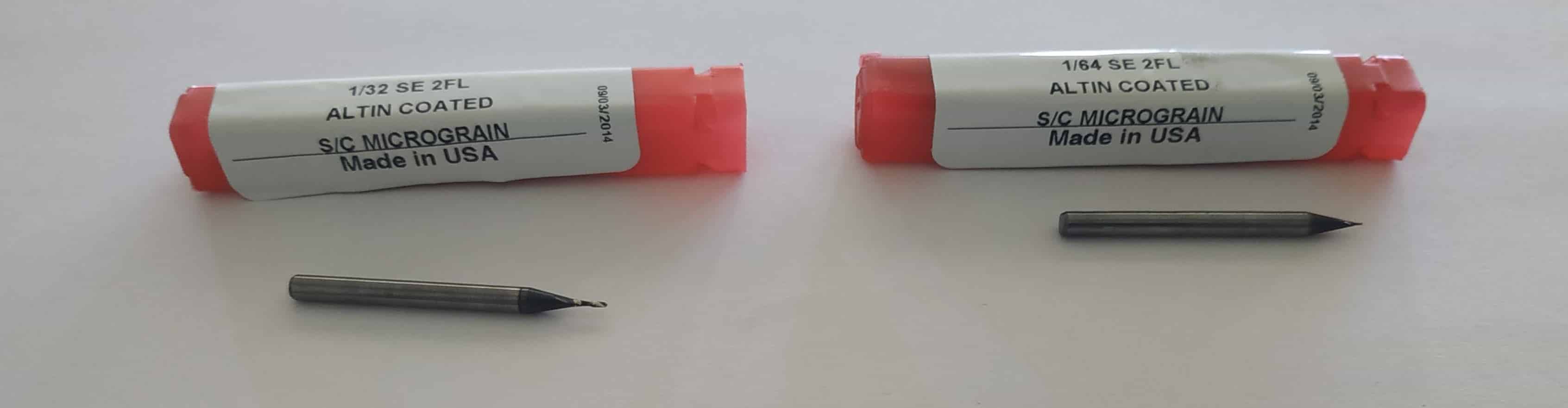
• Attached end mill 1/64 for milling traces
• Opened fab modules and upload my files there, then saved
• Setted the origin point chose"[Machine Coordinate System" in our case will use "G54" and "G55" that's the first 2 of 6 Work Coordinate Systems. During this process I used Vpanel pointers "right" "left" "up" "down"
Picture of endmills I used (1/64 and 1/32)
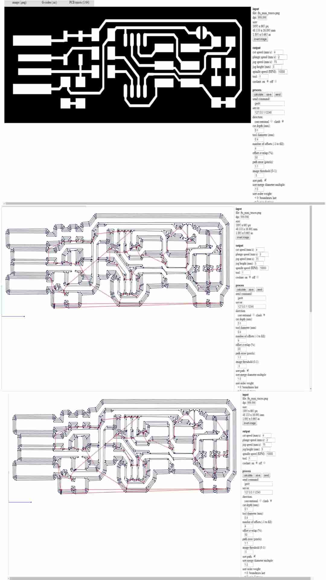
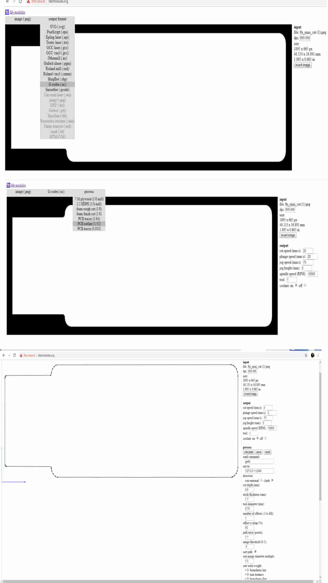
• Went back to fab modules and chose image "png"- Gcode "nc"-PCB traces "1/64" - "selected calculate" - "save"
Fab Isp traces
Fab Isp cut out
• Opened "cut" on vpanel and chose the cut file "Fab Isp traces" and start cutting
• When the traces were cut I repeat the process in fab modules for cuting out the the board, but that time I chose PCB traces "1/32"
• Cut out the board and cleaned up.
But after cleaning up the board I found out that the milling process had been failed, as parly the board was not milleed properly So I had to mill it again and set the "x,y,z" points again. The second try was successful.
Soldering
I have never soldered smd componets before, that's why I was very excited to do it.• Turned on soldering iron
• Selected the componets
I used the following components
• ATtiny45
• 1k resistors
• 499om resistors
• 49om resistors
• 3.3v zener diodes
• LED
• 100nF capacitor
• 2x3 pin header
• Started soldering of course I did many miastakes and demaged my fingers
• Cut another one board, as I demaged the first during soldering process. This process I repeated 3 times. The copper surface was striped.
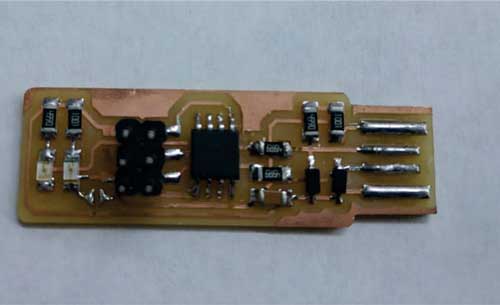
• Finally I soldered all components
Now the board is ready
Programming
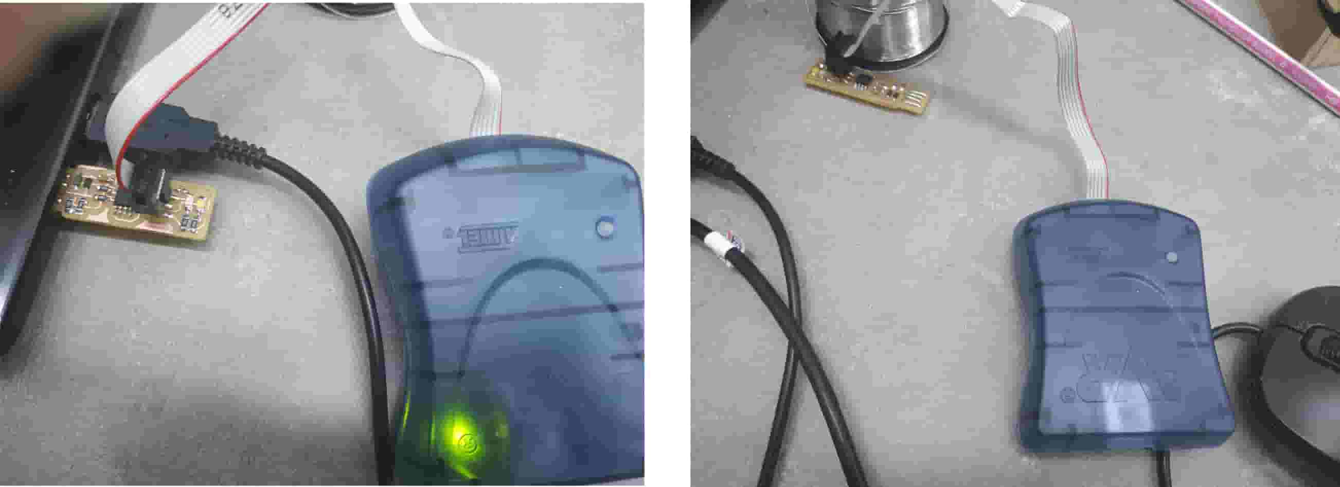
• Connected AVR programmer• Opened the terminal
• Wrote the command "sudo apt install avrdude gcc-avr avr-libc make"
• Downloaded firmware source code file
• Extracted firmware files
• Cd to the folder and write "make" command
• Then updated "makefile" with USB name, for that, run "gedit" in terminal, opened makefile in the firmware folder, edited the name "usbtiny" to "avrisp2". Finally saved the file
• Ran command "make flash"
• Ran "makefuses"
• Removed AVR and Attiny45 board, and pluged in Attiny45 board again
• Ran "lsusb comman", it showed ".Bus 001 Device 009: ID 1781:0c9f Multiple Vendors USBtiny"
Then removed AVR and TinyISP from system and insert it again in USB port, and my ISP did not work. I checked all connections by multyeter and foun odut that the controller did not work. I had to cut and solder the board again and this time I soldered it by lower temperature. Repeated all actiones described above and my ISP worked.
Conclusion
During this week I learned a lot of new things about• SRM-20 machine operation and milling
• Endmills, I read a lot of about different type of them
• PCB design
• Soldering SMD components
• Programmers and programming
And got painful injuries during soldering and learned about safety norms․
I needed to have Fab ISP in properly working condition as I would use it during next week for programming electronics board.