Electronics Production
Assignment
group assignment:
characterize the specifications of your PCB production process
individual assignment:
make an in-circuit programmer by milling the PCB, then optionally trying other processes
Group Assignment
For my part of the group assignment, I've researched the physical restraints and optimal settings for milling PCB's with our machines here at the lab.
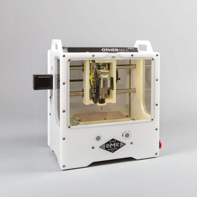
We have four OtherMill Pro's. The specifications as listed by the manufacturer are below:
260 × 254 × 324 mm
324 × 305 × 327 mm
140 × 114 × 40.6 mm
140 × 114 × 34.3 mm
7.62 kg
and 6061 aluminum
0.000125 in (0.003175 mm) microstepping
1,500 mm/min
25 microns
1,500 mm/min
200–240 V AC, 2 A
50/60 Hz
4–43 °C
Otherplan Classic
Windows 7 or higher
64-bit operating system required
Graphics card with OpenGL ES 2.0 support
Gerber RS-274X (.gtl and .grb)
G-Code (.nc and .tap)
SVG (.svg)
3.5 mm
0.25 mm
Regular
Double-sided
Maple
Brass
Aluminum, 6061
PVC
Acrylic
Delrin
For now all we are concerned with is milling pcb's, so we'll take a closer look at the recommended speeds and feeds. These are the default settings in the OtherPlan software:
Tool: 1/8" flat end mill
Feed rate: 14.173 in/min (360 mm/min)
Plunge rate: 1.81 in/min (30 mm/min)
Spindle speed: 12,000 RPM
Max pass depth: 0.005" (0.13 mm)
Tool: 1/16" flat end mill
Feed rate: 14.173 in/min (360 mm/min)
Plunge rate: 1.81 in/min (30 mm/min)
Spindle speed: 12,000 RPM
Max pass depth: 0.005" (0.13 mm)
Tool: 1/32" flat end mill
Feed rate: 14.173 in/min (360 mm/min)
Plunge rate: 1.81 in/min (30 mm/min)
Spindle speed: 12,000 RPM
Max pass depth: 0.006" (0.15 mm)
Tool: 1/64" flat end mill
Feed rate: 5.669 in/min (144 mm/min)
Plunge rate: 0.472 in/min (12 mm/min)
Spindle speed: 12,000 RPM
Max pass depth: 0.002" (0.05 mm)
Tool: 1/100" flat end mill
Feed rate: 5.669 in/min (144 mm/min)
Plunge rate: 0.472 in/min (12 mm/min)
Spindle speed: 12,000 RPM
Max pass depth: 0.002" (0.05 mm)
But if we look a little further, we find there is a way to create custom tools with specific speeds and feeds used when importing .brd or .grb files. The recommended "Advanced Speeds and Feeds" are as follows, from Bantam:
Tool: 1/8" flat end mill
Feed rate: 59 in/min (1500 mm/min)
Plunge rate: 15 in/min (381 mm/min)
Spindle speed: 16,400 RPM
Max pass depth: 0.006" (0.15 mm)
Tool: 1/16" flat end mill
Feed rate: 59 in/min (1500 mm/min)
Plunge rate: 15 in/min (381 mm/min)
Spindle speed: 16,400 RPM
Max pass depth: 0.006" (0.15 mm)
Tool: 1/32" flat end mill
Feed rate: 59 in/min (1500 mm/min)
Plunge rate: 15 in/min (381 mm/min)
Spindle speed: 16,400 RPM
Max pass depth: 0.006" (0.15 mm)
Tool: 1/64" flat end mill
Feed rate: 15 in/min (381 mm/min)
Plunge rate: 15 in/min (381 mm/min)
Spindle speed: 16,400 RPM
Max pass depth: 0.006" (0.05 mm)
Tool: 1/100" flat end mill
Feed rate: 8 in/min (203 mm/min)
Plunge rate: 5 in/min (127 mm/min)
Spindle speed: 16,400 RPM
Max pass depth: 0.002" (0.05 mm)
Design Rule List
Below are the Design Rule Considerations provided by Bantam tools.
The Othermill Pro and Bantam Tools Desktop PCB Milling Machine have the same design rules.
- Minimum trace width: 6 mil for Othermill Pro, 10 mil for Othermill
- Minimum trace spacing: 6 mil for Othermill Pro, 10 mil for Othermill
- Minimum via/pad annular ring thickness: 6 mil for Othermill Pro, 10 mil for Othermill
- Minimum drill size: 16 mil (or smaller with non-standard bits)
- Minimum SMD pad size: 6 mil for Othermill Pro, 10 mil for Othermill
- Polygon isolation value: 1 mil larger than the largest tool you want to use
- Route traces to through-hole pins on the bottom side only (holes are not plated)
- Slotted/oval holes are not supported
Spacing Between Traces and Components
When designing circuit boards to mill on the Bantam Tools Desktop PCB Milling Machine, Othermill, or Othermill Pro, it’s important to consider the distance between each element of your board because the spacing between elements dictates the size of the tool you’ll need to mill them.
For example, if you’d like to use a 1/32" Flat End Mill, your traces, pads, vias, etc. need to be greater than 0.03125" apart. You can use smaller tools, like a 1/64" or 1/100" Flat End Mill, which will allow you to place objects closer together. However, the trade-off is that smaller tools take longer.
The same holds true for vias and through holes — the inner diameter of each hole needs to be larger than the tool you’re planning to use to drill it. If you’re unsure as to whether some elements are too close together, you can test it by importing your files into the software and seeing how it looks.
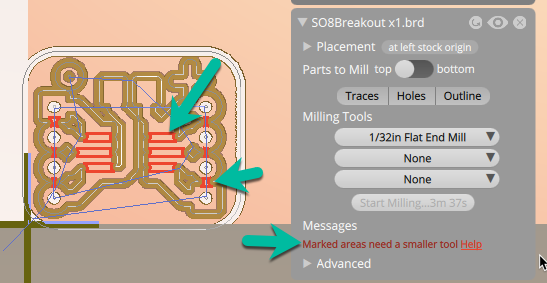
The spacing between traces is too small for the chosen end mill.

By selecting a smaller tool, now the chosen end mill can fit in the spacing.
If you’ll be using surface-mount (SMD) components, the pads need to have enough space between them for the tool to fit. Check the list of millable packages in the Surface-Mount Package Compatibility Guide to make sure the package you want to use can be milled.
If your package isn’t listed, you can determine if it can be milled in one of two ways.
1. You can test if it will work by loading your .brd file or Gerber files into our software, selecting a cutting tool, and looking to see if there are red warnings lines. The red warning lines indicate that the design feature is too small to be milled with the currently selected cutting tools. Try selecting a PCB Engraving Bit 0.003", a 1/32" Flat End Mill, and a 1/64" Flat End Mill. If you don't see red warning lines, then the package can successfully be milled!
2. Find the diagram showing the dimensions of the package you want to use. Find the smallest pad size, and find the smallest space between features. If this smallest size is 0.006" or larger then the package can be milled with the Bantam Tools Desktop PCB Milling Machine and Othermill Pro. If the smallest size is 0.010" or larger then the package can be milled with the Othermill.
Keep in mind that when milling features under 0.010" it's important to use follow a precise workflow, which includes using high-strength double-sided tape, the high-precision collet set, using digital calipers to measure PCB blank thickness, and using sharp end mills.
Vias
If your board has vias (electrical connections between the front and back of the board), you’ll need to create a connection between them by hand when you solder the board. For this reason, we recommend minimizing the number of vias and through-hole connections you use in your board.
The simplest way to connect a via is to put a short piece of wire through the via hole and solder both ends, but you can also use via eyelets (aka rivets), which sit neatly in the holes as you solder them. Just make sure your eyelets fit your holes. A third option, which is often the fastest, is to take a long piece of tinned wire and thread it through all the vias in your board. Then solder all the vias and snip off the excess wire.
PCB software autorouters will often use through-hole pins as vias. This presents a problem when you use components that can’t be soldered easily on both sides of the board, such as pin headers. To avoid this issue, draw polygons in the Restrict layers over the areas you want the autorouter to avoid. In EAGLE, for example, these are the tRestrict (41), bRestrict (42), and vRestrict (43) layers.
Ground/Power Planes
If your file is designed with a ground or power plane, check to make sure that your polygon isolation value is set to at least the width of the smallest tool you’re going to use on the milling machine. If the isolation is set to zero, which is often the default in PCB design software, the tool will not fit between the ground/power plane and the traces. If your design allows for it, setting the polygon isolation to the width of your largest tool will greatly speed up the milling process. For example, if your design has a few tiny features that need to be milled with a 1/100" tool, but most of the other features can be milled with a 1/32" tool, setting your polygon isolation to 0.032" instead of 0.011" will allow you to use a 1/32" tool for most of the board, which is much faster than using a 1/100" for the whole board.
Trace Width
The minimum trace width we suggest is 6 mils (0.006") for the Bantam Tools Desktop PCB Milling Machine and Othermill Pro, 10 mils (0.010") for Othermill because thinner traces are more likely to delaminate from the board. We suggest using the widest traces your design can support.
Likewise, annular rings for through holes and vias should be at least 6 mils for Bantam Tools Desktop PCB Milling Machine and Othermill Pro, 10 mils for Othermill (outer diameter minus inner diameter).
Slotted/Oval Holes Not Supported
The software doesn’t support the G85 command which is used to make slotted/oval holes. If you need a slot, make a row of overlapping holes that are a few thousandths of an inch larger than the tool and overlap by about half their diameter (i.e. for a 1/32" (0.031") tool, make a row of 0.033" holes, with centers spaced 0.016" apart).
Ways to Increase Milling Speed
Larger end mills mill faster than smaller ones, so you can increase milling speed by spacing out your components, traces, and holes such that they can all be milled or drilled by a 1/32" or larger end mill.
Minimize the use of 1/64" and 1/100" End Mills by using rounded corners instead of angles. The software takes time to mill the innermost angle, where a 1/32" can’t reach, which is helpful in some situations but not here. The corner radius needs to be larger than 0.03125" for this to work with a 1/32” End Mill.
Still want to go faster? Check out our Custom Tool Library guide to learn how to change the feeds and speeds.
DRC (Design Rule Check) Files
If you’ve never used DRC files, they help you find layout-related problems with your board, such as components or traces that are too close together.
There are currently DRC files for EAGLE, which you can download from the EAGLE page.
Final Thoughts On PCB Design Rules
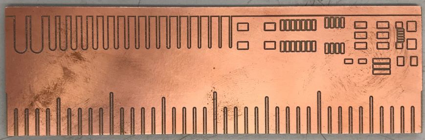
While a 6mm trace can in theory be made on the othermill. I've found that traces that small often break and delaminate from the substrate. The minimum reliable trace size seems to be 10. I've found 12 mil to give a little extra room for mistakes, but still be small enough to fit between most pads.
In addition to designing traces no smaller than 10 mil, I've found that the 80 degree engravig bit has given the cleanest and most reliable traces (no fuzzy copper on the edge of traces) and allowed for the smallest features to be milled.
For vias, I've found a drill pattern with the 1/64" endmill to work well so that I can use thin wire to stitch the two sides of the board together
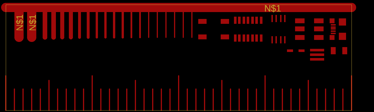
I put together this ruler to test the design rules from Bantam Tools.
The milling bit is an 80 degree metal engraving bit.
Cutting depth set to .15mm and there is a .2mm trace offset
Individual Assignment
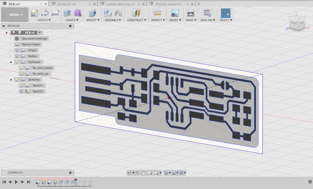
So I've built a lot of things, but I have no experience making circuit boards. I know EagleCAD is the autodesk's specific PCB design, CAD, and CAM software. I downloaded it and watched a couple tutorials but am still a little overwhelmed by the program and my lack of electronics knowledge, so I opted for just using other methods to get this board milled. A PNG file of the traces and board outline was all Brian's tutorial provided. I realized that I could probably trace the image in Inkscape and import the SVG to Fusion, but I wanted to trace it by hand in Fusion, to get a little more experience with the program.
UPDATE: Using FabModules was definitely the easiest, quickest way to get g.code for the PCB mill. That process is outlined further down the page.
Tracing
The calibrate feature for images in Fusion is very convenient and easy to use. I found references for the lead spacing on the ATiny45 that's specefied as well as for the spacing on the USB pads. I calibrated the canvas using the ATiny spacing and confirmed that scaling by measuring the USB pad spacing. Everything was within a couple thousands of a millimeter, well within tolerance.
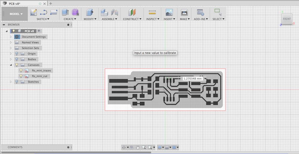
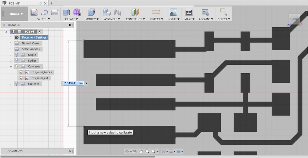
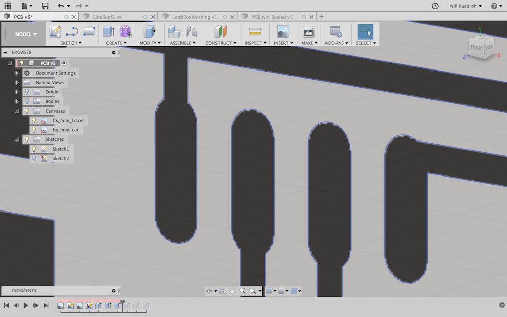
I really like the "smart snapping" in the Fusion sketch environment. It made the tracing a bearable experience. Once a few corners and lines have been layed out, most other geometry is in line with previously placed geometry and the snaps make the process intuitive and the drawing very regular.
Below is a short screen recording of the smart snapping that made sketching in Fusion so bearable. I would have recorded more of the process, but screen recording and running Fusion at the same time on my computer made things unbearably slow.
Modeling/CAM
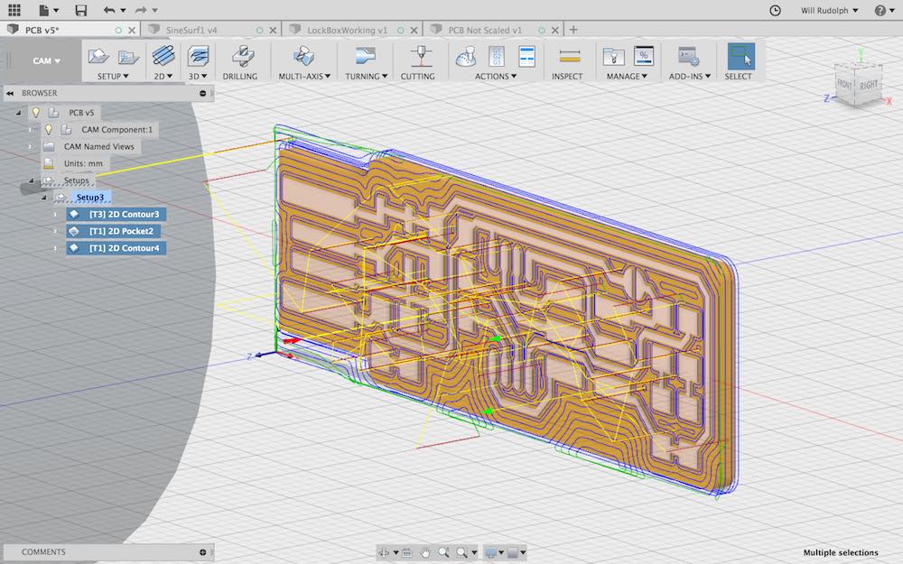
I was thinking about 3D printing some kind of case for this board, so I figured I'd model everthing to size from the beginnning. That way I can also simulate all the milling in Fusion and make sure nothing will go awry. I think you could also just make the toolpaths from the sketches, but I've been frustrated trying to do that in Fusion before.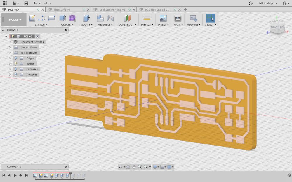
For the correct speeds and feeds in Fusion, I used the advanced feed rates for the 1/64" and the 1/32" endmills, making sure to secure the material very well and make sure everything was level.
Using FabModules
This made the process a lot more simple and streamlined. Took a little time to get used to navigating. Had luck with fabmodules.org not with mods.cba.mit.edu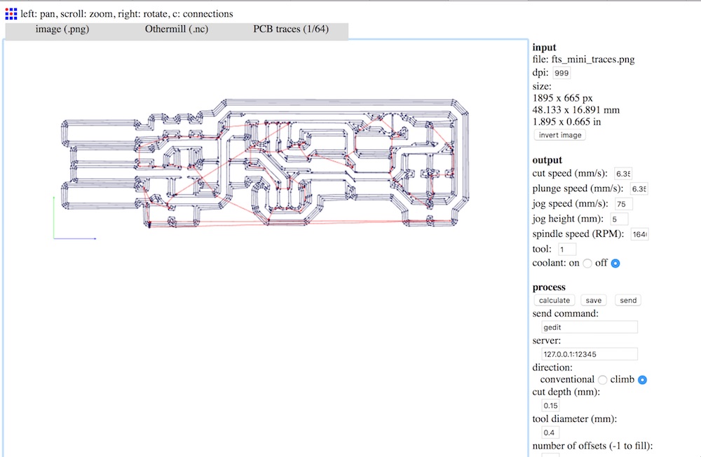
Milling
So our Lab's equipment for producing PCB's is the OtherMill Pro, a small desktop multipurpose CNC's with the required resolution for milling circuits. We have one sided FR-1 boards that seem to measure about 1.55 mm thick, 1.65-1.7 mm with double sided tape applied. We have 1/64th, 1/32nd, 1/16th, and 1/8th two-flute, flat-bottomed, carbide endmills available for these machines.
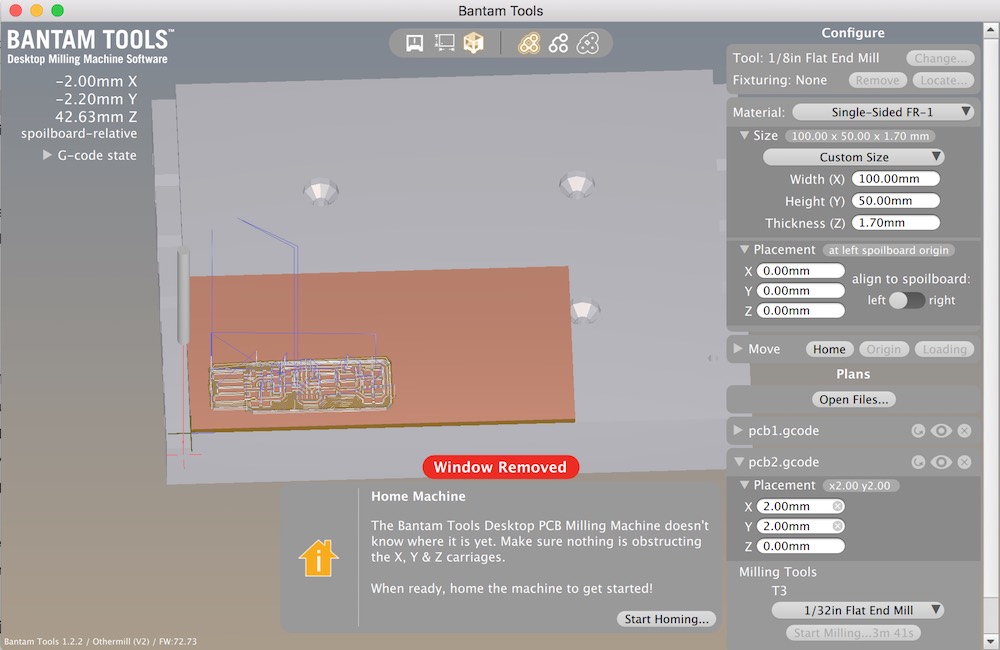
Othermill's proprietary software, Otherplan is quite intuitive and easy to use.
First, I began by entering the stock thickness, (including the thickness of any tape or attachment material) 1.7 mm. The xy size of the material is not essential to have exact for our purposes, I set it to 50 x 100 mm. This is such a small board, I'm going to use scraps of old pieces of FR-1 to mill. Otherplan very nicely shows a 3D rendering of the milling table with the stock shown at the size that is entered. Then when we load our .nc or .gcode files and choose a milling bit, the toolpaths and stock removed are simulated and shown on the material. This is very handy for confirming that everything looks as it should in our file. Homing the machine, changing out and locating new bits is as easy as following prompts from the OtherPlan software.
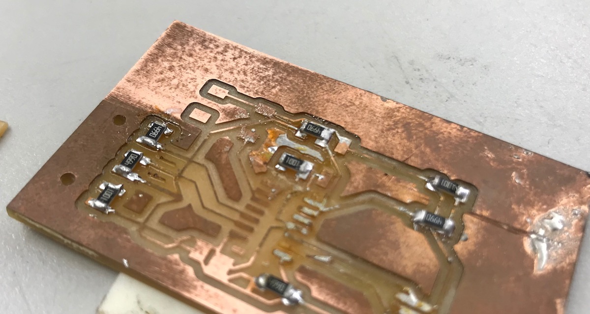
Though FabModules made generating the .gcode from the .png much easier, it limited my ability to alter toolpaths, and since I already had PCB modeled in Fusion, I figured I'd go with the toolpaths I created, rather than those generated by FabModules. Partly because we only had two 1/64th inch endmills left and I was the first to mill, so I didn't want to risk breaking anything. Taking that into account, I only ran a single tracing path with the 1/64th inch bit. For the rest of the stock I removed with a 1/32 bit. I just pocketed the remaining area to remove all of the copper. I havent seen any other boards that do this. I assume one ususally only mills around the traces simply to save time and cut down on tool wear. Finally, for the final outline cutout, I used a 1/16th inch endmill.
I was a little terrified starting the milling process I didn't want to break any endmills and we were already low on them. I though everything would go to plan, I had watched the simulation run in fusion, double checked all my measurments, double checked all my input values, and finally started the file for the traces. The first plunge was an anxious moment, but once the bit started milling everything looked like it was going well. After a few more moves and plunges I became comfortable with the macine running at the set speeds and feeds. The sound was quite nice (in the sense that I heard no undue vibration, chattering, straining, just smooth cutting. All the traces looked like the appropriate size, tiny. I switched out the 1/64th inch bit for the 1/32nd and continued on to run the next file that would clear out the remaining copper. Finally, I switched out for the 1/16th inch endmill to cut the board outline. I wanted to run through the process once more to get further aquainted with PCB work and to make a second board in case of catastrophic failure of the first. One thing I noticed while running the files on the first board is that if the board were cutout first, it would eliminate some of the material that was being cut by the 1/32nd bit. I figured less tool wear on the tiny bit would be better. Everything went smoothly again. I was so wrapped up in the excitement of the process and things going well that I did not take any photos or videos of the milling process.
Soldering
So I enjoy very detailed craft work and figured surface mount soldering would be a nice exercise in such work. I found this video (below) that gives a very nice overview of the principals and practices of soldering. It's a little dated, no surface mount parts, but does a very good job of explaining what good and bad solder joints look like and how to achieve them.
I got so concentrated and focused soldering that I forgot to take any videos or pictures along the way again. I kept in mind a lot of advice I've gotten over the years concerning detailed handwork:
-keep breathing calmly
-perform the actions taking the most concentration/stillness as you breathe out
-Keep a light grip on the your tools (soldering iron and tweezers), just enough to hold something and no more
-Move the workpiece constantly to find the best location and approach
-Check your work as you go
-Check your work when you're done
-Walk away, come back, and check your work once more with fresh eyes
I added the last piece of advice after I realized while looking at a picture of my board that I had completely missed solder on one pad. For very small detailed work such as this, looking at a photograph was incredibly helpful to check out things up close. The missing solder really jumps out in the last photo.
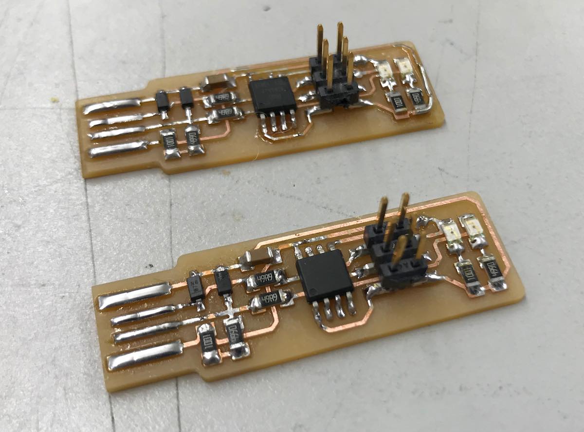
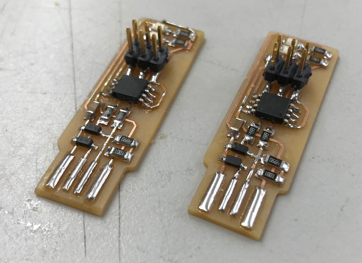
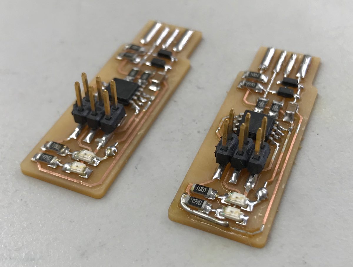
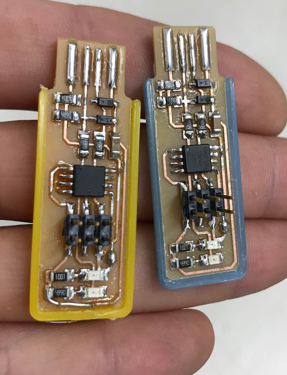
So I made two boards, assuming I'd make some mistakes while soldering, but surprisingly, the first one came out better than the second. Since I already had the fusion model, I quickly extruded a couple sketch elements to make a simple "case" and had a .stl ready to 3D print. With the cases attached, the boards fit snugly into a usb port. If you'd like to make your own, the .stl is included in this weeks files linked below.
Programming A Board
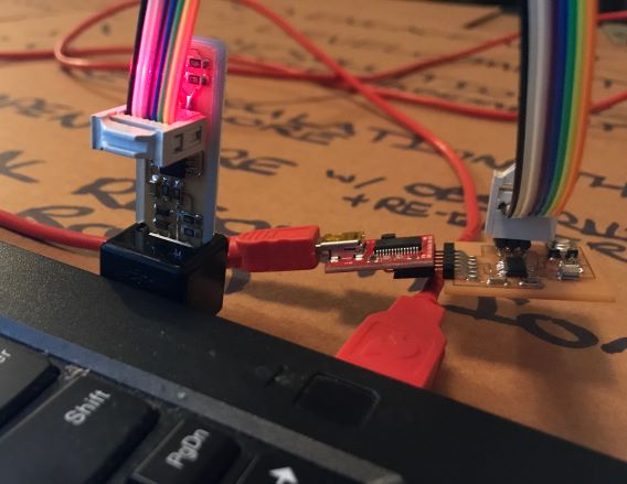
So I missed documenting the original flashing of my usbtiny programmer, but it is still in use, and I figured I'd show how to flash another microcontroller with it using the same techniques. The process is well documented in Brian's aforementioned page, but I'll show how I did it.
        Windows PowerShell
Copyright (C) Microsoft Corporation. All rights reserved.

Try the new cross-platform PowerShell https://aka.ms/pscore6

PS C:\Users\will.rudolph> cd .\Desktop\Blink\
PS C:\Users\will.rudolph\Desktop\Blink> make
avr-objcopy -O ihex blink.out blink.c.hex
avr-size --mcu=attiny44 --format=avr blink.out
AVR Memory Usage
----------------
Device: attiny44

Program:     684 bytes (16.7% Full)
(.text + .data + .bootloader)

Data:         18 bytes (7.0% Full)
(.data + .bss + .noinit)


PS C:\Users\will.rudolph\Desktop\Blink> make program-usbtiny
avr-objcopy -O ihex blink.out blink.c.hex
avr-size --mcu=attiny44 --format=avr blink.out
AVR Memory Usage
----------------
Device: attiny44

Program:     684 bytes (16.7% Full)
(.text + .data + .bootloader)

Data:         18 bytes (7.0% Full)
(.data + .bss + .noinit)


avrdude -p t44 -P usb -c usbtiny -U flash:w:blink.c.hex

avrdude: AVR device initialized and ready to accept instructions

Reading | ################################################## | 100% 0.06s

avrdude: Device signature = 0x1e9207
avrdude: NOTE: FLASH memory has been specified, an erase cycle will be performed
         To disable this feature, specify the -D option.
avrdude: erasing chip
avrdude: reading input file "blink.c.hex"
avrdude: input file blink.c.hex auto detected as Intel Hex
avrdude: writing flash (684 bytes):

Writing | ################################################## | 100% 1.27s


avrdude: 684 bytes of flash written
avrdude: verifying flash memory against blink.c.hex:
avrdude: load data flash data from input file blink.c.hex:
avrdude: input file blink.c.hex auto detected as Intel Hex
avrdude: input file blink.c.hex contains 684 bytes
avrdude: reading on-chip flash data:

Reading | ################################################## | 100% 0.79s


avrdude: verifying ...
avrdude: 684 bytes of flash verified

avrdude: safemode: Fuses OK

avrdude done.  Thank you.

PS C:\Users\will.rudolph\Desktop\Blink>
To download my files click here: