Final Project M2
This website, along with all of the documentation hosted on it, will stay up for quite a while. Because of this, I want to keep on using the site to document my other fabrication projects that I make with what I have learned from this class. I feel like this will be quite fitting, because one of the last things I wrote in the “about me” page of my site many months ago was that, “I can’t wait to see what’s possible for me in the future.” Well, here we are. Now that I’ve finished up the class, I’m going to use all of the skills that I have learned to make even more fun and cool projects in the future, and so therefore I want to document those projects here, where the journey all began.
Even though I have already globally presented my final project this morning, I’m not done working on it. Over the summer, I plan to keep on revising it until it’s something that I’m actually proud of, not just something that gets me through the class. (Not that I don’t like how my final project turned out, I just know I could have done it better).
Also, one more thing to note. Since I’m technically done with documentation for the class itself, and since this is now for my own enjoyment more than anything else, I won’t be going into quite the same rigorous level of detail on everything.
What Will Be Different
My main goal for the reactive light display now is to put the “control box” and the display together. Rather than using tons of connection wires between the two halves of my project, I can just put it all on the same board and it should come out much cleaner.
The other thing that I’m going to do is a little unorthodox when compared to what I have done for Fabacademy in the past. Rather than milling out the boards myself and dealing with broken bits or ripped up traces, I’m going to design the boards in EagleCAD, then have them sent off to be commercially manufactured. I think this is now ok to do since I’ve already proven time and time again that I know how to mill out my own boards, and since oftentimes a commercially made board will hold up much longer than one that I could make in the lab.
The New Board
I went ahead and made a new schematic/board in Eagle that had both the sensors and the LEDs on them. Here’s what that looks like below.
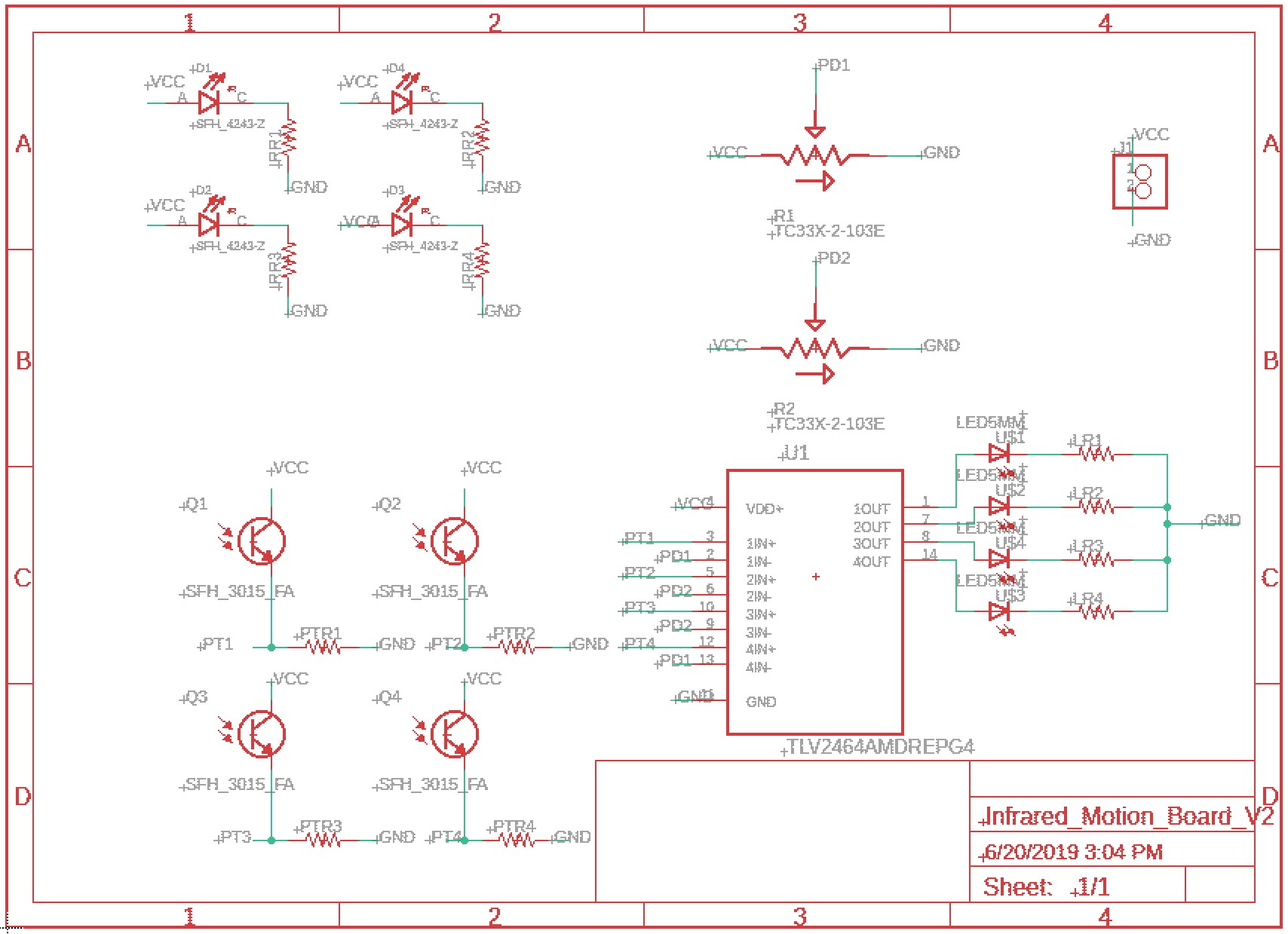
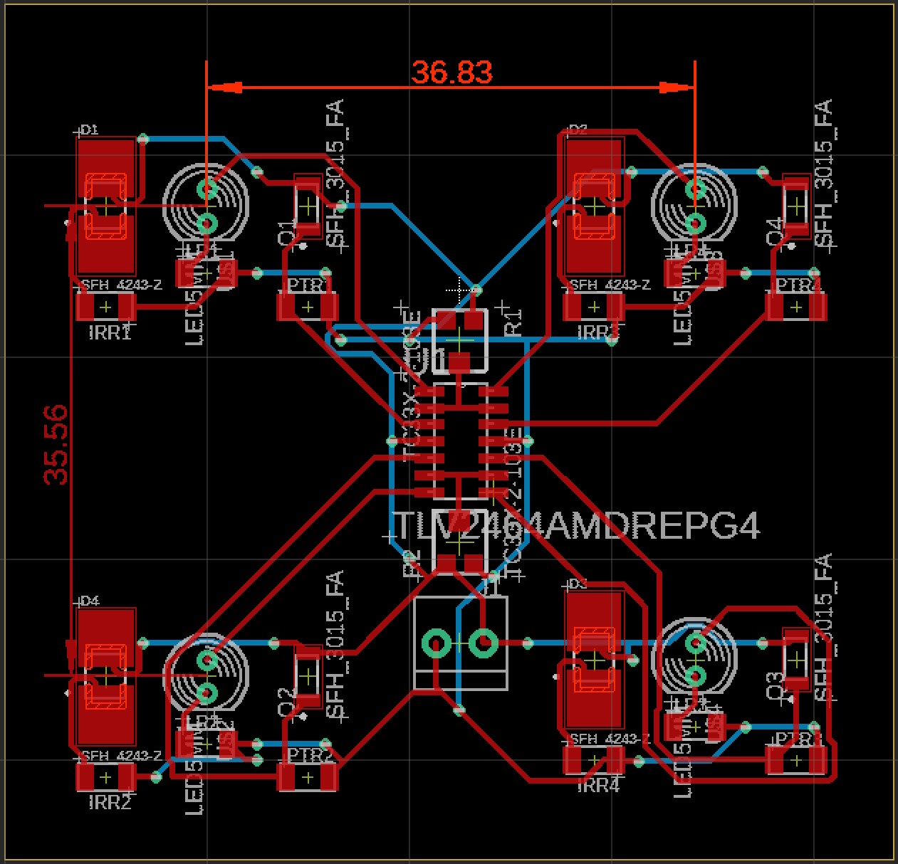
You may notice that this board looks a little different from how they usually do, and that’s because I’m going to be using a two sided PCB this time. There are both red and blue traces on the .brd file for the top and bottom traces of the board.
Sending the Board Files
You might think that since I’m having the boards made elsewhere, it’s as easy as clicking a few buttons and waiting for them to arrive. While it is certainly an easier process than milling out the bards myself, that doesn’t mean that I’m not learning anything new in the process.
I’m going to be ordering my PCBs from a company called JLCPCB that’s located near Shenzhen, China, and my first learning curve came when I needed to upload the files for them to use during board production. Rather than just directly sending them my EagleCAD “.brd” file like I always did in Bantam Tools, (that’s our lab’s milling machine software), I had to upload something called “Gerber Files”.
At first, I had no idea what they were talking about because I had never seen this file type before. After some research, though, I learned that this is the standard file type for PCB manufacturing, and that it can include copper traces, soldermasks, silkscreens, and more. Then, I later found a video that explains exactly how to obtain these files from Eagle, and the video even seems tailored to JLCPCB specifically.
I followed the tutorial above and had my files ready to go within a few minutes. Here’s a short summary of the steps in that process.
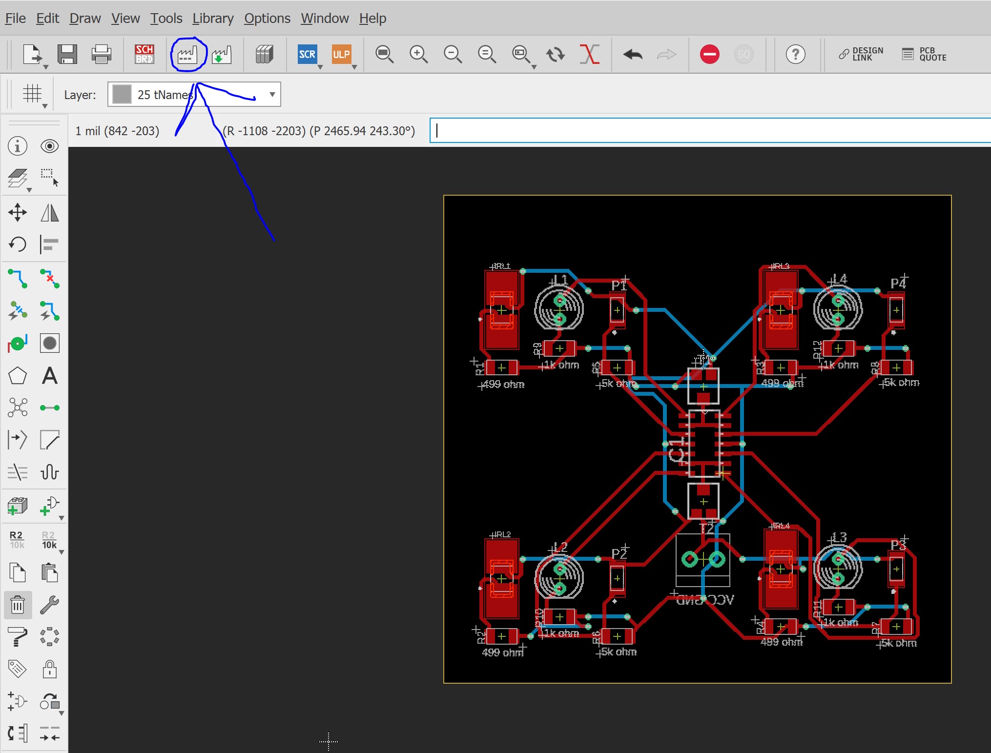
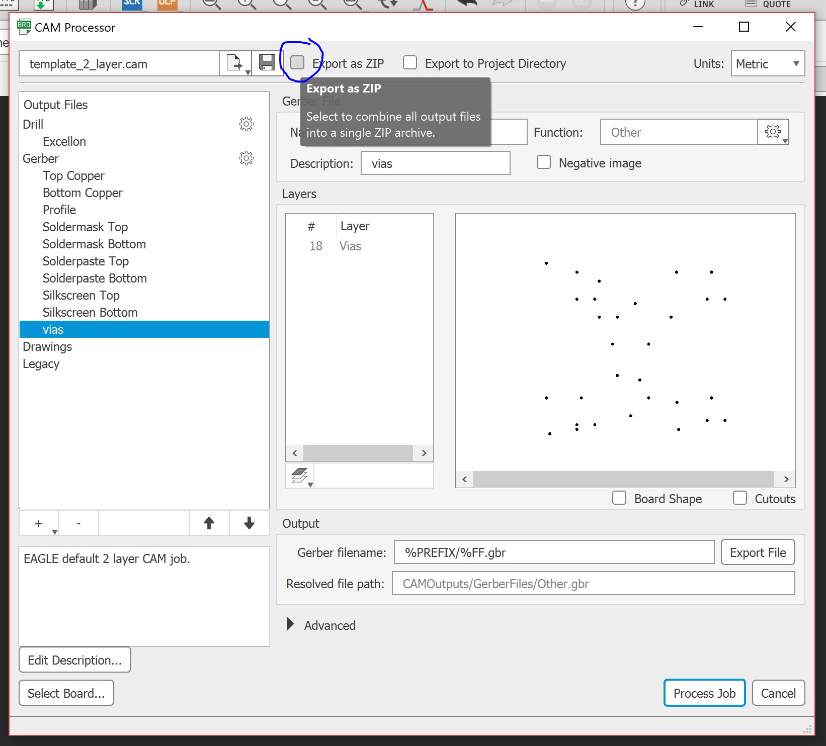
1: Open up the CAM Processor in Eagle.
2: Add a “new Gerber output”, name it “vias”, and select the layer called “vias”.
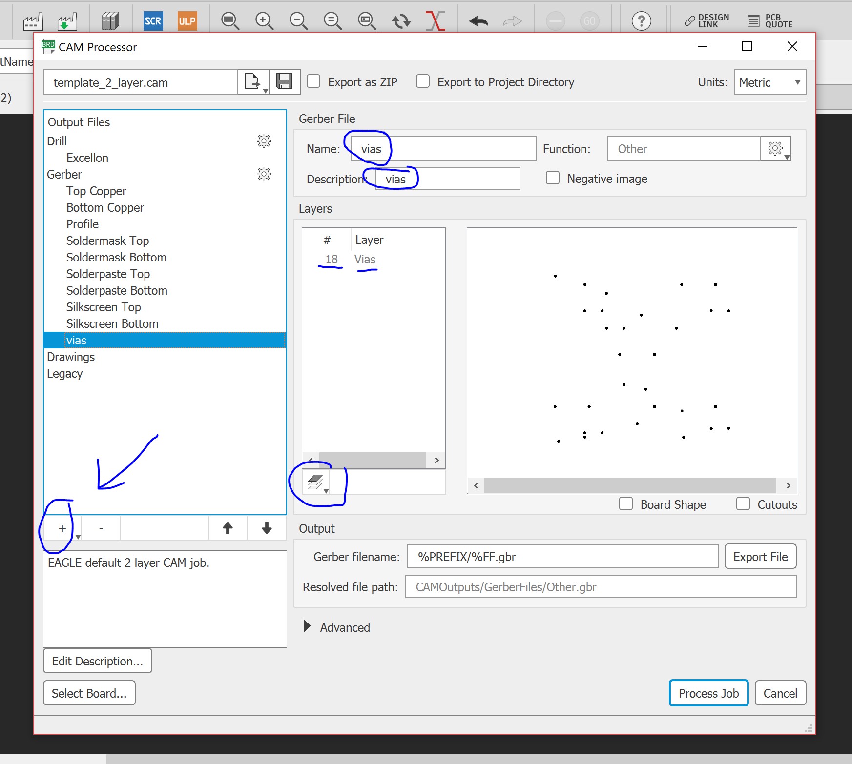
3: Check the box that says, “export as ZIP”, then click, “Process Job” and the files should be ready.
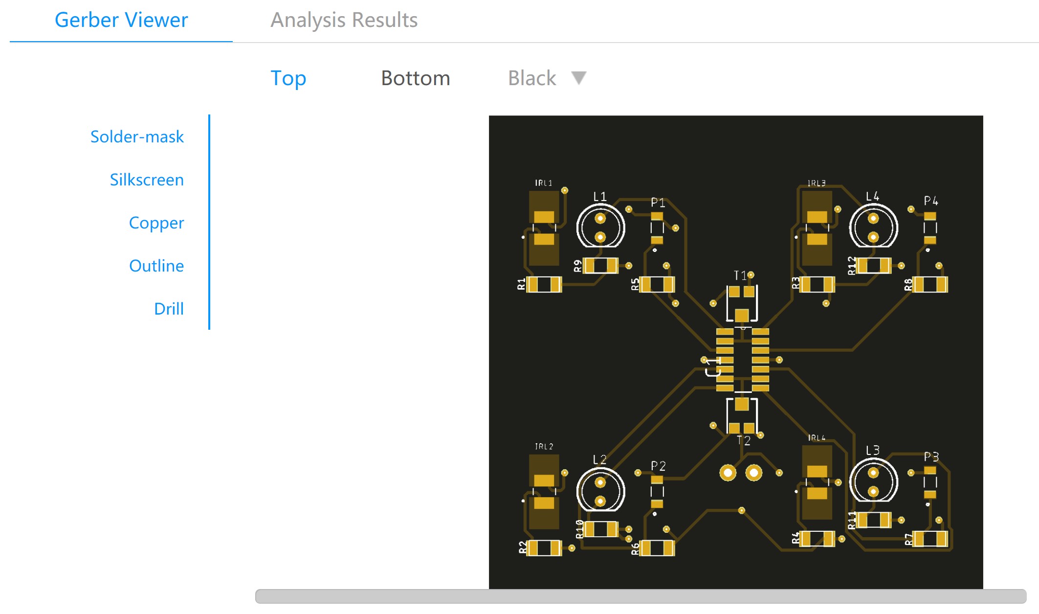
Once I had the files, I uploaded them to the manufacturer’s website. Then after that, I ran into the first benefit of having commercially made boards, being able to pick the color. I got to choose from green, red, blue, black, and white, and I ended up going with black since that will also be the color of the 3D printed housing. It also gave me an estimated output of what the board will look like.
Board-Specific Vocabulary
One last thing about the boards. You may have noticed above when I used words like “silkscreen” and “solder mask” when I was talking about the Gerber files. At first, those words were just more unknown manufacturing lingo to me, but I’m now realizing what it actually is. The reason that I didn’t know what these meant before now is that I just never had a need to learn them. You see, the boards that we can make in the lab, while still being quite effective, don’t have the same capabilities as those that are commercially manufactured. That means that none of the boards we make will have solder masks, solder pastes, or silkscreens.
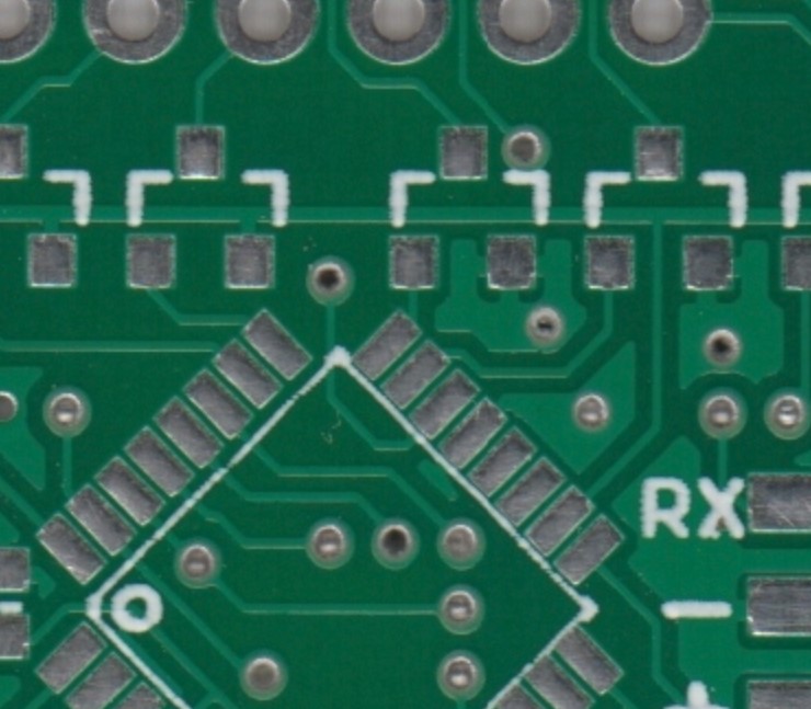
Commercially made boards, on the other hand, can be made with what’s called a solder mask on top of them. Have you ever seen the really stereotypical green circuit boards on tv, in pictures, or even in person? You probably have, but just in case, here’s one below.

You see, the green color doesn’t actually come from the board itself. Rather, it is caused by a thin green layer of solder mask on top of either side of the board. If you could peel back the green layers, you’d see that the rest of it is much more plain underneath. Also, green is the most common color to use for these soldermasks, but that doesn’t mean there aren’t others out there. My own boards, for example, are being made with a black solder mask, not a green one, so that they can match the color of the PLA frame around them.
This solder mask helps to protect the copper traces beneath while also keeping the whole board in good shape over longer periods of time. The only issue with this is that they can’t put soldermasks over the component’s pads because that wouldn’t allow you to actually solder the components to the board, and this is what leads us to the solder paste.
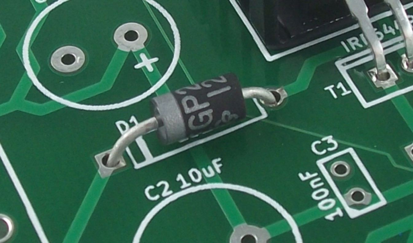
When they manufacture these boards, they make them out of the same basic copper as we do here. However, any exposed copper will eventually tarnish and start to corrode with time, so commercially, they can’t just leave the pads for the components exposed to the air around them. Instead, they apply what’s called solder paste to the pads and melt this down with a hot air gun. The solder paste then flows onto the pad and covers it up from the outside air, (that’s why the pads on commercial circuit boards aren’t copper colored, they’re the color of solder), and this also makes the pad a little easier to solder components onto due to the solder that’s already there. Below, you’ll find an example of what this solder paste can look like.
Lastly comes the silkscreens. They’re probably the easiest to understand out of this bunch, largely due to their simplistic purpose. On any commercial board, you’ll most likely find some sort of white lines and lettering located near or around the components. This is called the silkscreen, and it’s used to help people know where to place components on the board. It’s made using non-conductive ink so that you never have to worry about it affecting the performance of the board, and it’s honestly quite helpful to have when you’re dealing with so many small parts that all look the same.
3D Printing
Next up, I began designing the new 3D printed housing for my project based on the dimensions of the new boards. I started in my favorite software, Fusion360, and got to work. Below you’ll find a rough estimate of what it will look like, I’ll make a more accurate one once the boards come in.