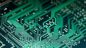
What is PCB?
It stands for "Printed Circuit Board.". A printed circuit board (PCB) mechanically supports and electrically connects electronic components or electrical components using conductive tracks, pads and other features etched from one or more sheet layers of copper laminated onto and/or between sheet layers of a non-conductive substrate. Components are generally soldered onto the PCB to both electrically connect and mechanically fasten them to it.
Types of PCB
There are various types of PCB on based of their construction :
Raster images are made of pixels.
A pixel is a single point or the smallest single element in a display device.
If you zoom in to a raster image you may start to see a lot of little tiny squares.
Single Sided PCB
This type of printed circuit board contains just one layer of substrate, or base material. One side of the substrate is covered with a thin layer of metal, typically copper because it’s an excellent electrical conductor.
This type of board works best for simple electronics, and at-home hobbyists often design and construct this type of board first. Single-sided boards tend to cost less to mass-produce than other board types. But despite this low cost, they’re used infrequently because of their inherent design limitations.
Double Sided
Double-sided PCBs are much more common than single-sided boards. Both sides of the substrate have metal conductive layers, and parts are attached to both sides as well.
Double-sided circuit boards connect the circuits on each side using one of two methods: through-hole technology and surface mount technology. Through-hole technology involves feeding tiny wires, known as leads, through the holes and soldering each end to the appropriate component or circuit.

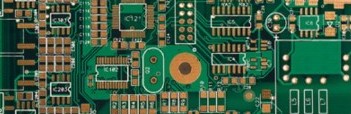
Multi Layered
Multilayer PCBs expand on the technology used in double-sided boards. They have several layers of substrate boards, and insulating materials separate the individual layers. As with double-sided boards, components on multilayer boards can connect to each other through holes, or vias, in the board.

Typical multilayer boards have 4, 6, 8, or 10 layers, but they can have more, depending on the demands of the product the board is intended for.
Rigid PCB
In addition to having various numbers of layers and sides, PCBs can also come in varying rigidities. Most consumers typically think of rigid PCBs when they picture a circuit board. Rigid PCBs use a solid, inflexible substrate material such as fiberglass that keeps the board from bending. (Eg. Motherboard)
Flex PCB
The substrate in a flex PCB is usually a flexible plastic. This underlying material allows the board to fit into shapes that rigid boards cannot and to bend or move during use without damaging the circuits on the board.
They cost more than Rigid PCBs but also has advantages. For example, they can replace heavy or bulky wiring in advanced equipment, like satellites, where weight and space matter. Flex PCBs can also come in single-sided, double-sided, or multilayer formats.
Rigid Flex PCB
These boards combine technology from both rigid and flex circuit boards. A simple rigid-flex PCBs consists of a rigid circuit board that attaches to a flex circuit board. Rigid-flex boards can be more complex if design needs demand.

PCB Mounting
The technology used in PCB is classified into two types as follows.
SMT (Surface Mount Technology)
Surface-mount technology (SMT) is a method for producing electronic circuits in which the components are mounted or placed directly onto the surface of printed circuit boards (PCBs). An electronic device so made is called a surface-mount device (SMD). In the industry it has largely replaced the through-hole technology construction method of fitting components with wire leads into holes in the circuit board.
An SMT component is usually smaller than its through-hole counterpart because it has either smaller leads or no leads at all.
Through-Hole
"Thru-hole", refers to the mounting scheme used for electronic components that involves the use of leads on the components that are inserted into holes drilled in printed circuit boards (PCB) and soldered to pads on the opposite side either by manual assembly (hand placement) or by the use of automated insertion mount machines.
Through-hole components are best used for high-reliability products that require stronger connections between layers.
Components Of PCB
Switch
Switches can come in many forms such as pushbutton, rocker, momentary and others. Their basic function is to interrupt electric current by turning a circuit on or off.

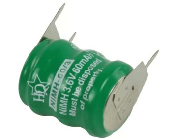
Battery
Provides voltage to the circuit.
Resistor
They control the electric current as it passes through them. They’re colour coded to determine their value. The value is measured in Ohm.
You can use a multimeter or Digikey’s resistor color code calculator to determine the value of a resistor.

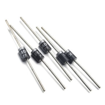
Diode
A diode allows electricity to flow in one direction and blocks it from flowing the opposite way.
The diode’s primary role is to route electricity from taking an unwanted path within the circuit.
It flows current from Anode (+) to Cathode (-).
LEDs
light emitting diode. Lights up when current flows through it, and will only allow current to flow in one direction.
Integrated Circuits
An integrated circuit is a circuit that's been reduced in size to fit inside a tiny chip.
This circuit contains electronic components like resistors and capacitors but on a much smaller scale.
Integrated circuits come in different variations such as 555 timers, voltage regulators, microcontrollers and many more. Each pin on an IC is unique in terms of its function.

Transistors
It amplifies current.
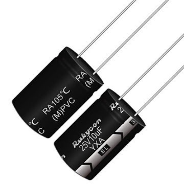
Capacitors
Capacitors store electricity and then discharges it back into the circuit when there is a drop in voltage. A capacitor is like a rechargeable battery and can be charged and then discharged. The value is measured in F (Farad), nano Farad (nF) or pico Farad (pF) range.
Relay
A relay is an electrically operated switch that opens or closes when power is applied. Inside a relay is an electromagnet which controls a mechanical switch.

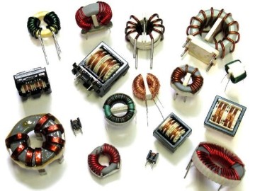
Inductors
Stores charge and stops and change in current.
Electrical Diagrams
There are essentially two types of electrical diagram :
Schematics
These diagrams use symbols to illustrate what electronic components are used and where they’re placed in the circuit. These symbols are graphic representations of the actual electronic components.
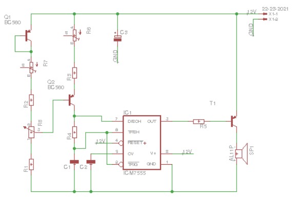
Board Diagrams
This is an actual represenntation of the circuit.

What is an ISP?
In-system programming (ISP), also called in-circuit serial programming (ICSP), is the ability of some programmable logic devices, microcontrollers, and other embedded devices to be programmed while installed in a complete system, rather than requiring the chip to be programmed prior to installing it into the system.
The primary advantage of this feature is that it allows manufacturers of electronic devices to integrate programming and testing into a single production phase, and save money, rather than requiring a separate programming stage prior to assembling the system.
This may allow manufacturers to program the chips in their own system's production line instead of buying preprogrammed chips from a manufacturer or distributor, making it feasible to apply code or design changes in the middle of a production run.
FabISP
The FabISP is an in-system programmer for AVR microcontrollers, designed for production within a FabLab. That is, it allows you to program the microcontrollers on other boards you make, using nothing but a USB cable and 6-pin IDC to 6-pin IDC cable.
It's based on the USBtiny and V-USB firmwares, which allow the ATtiny44 to perform USB communication in software. Programming can be done through avrdude.
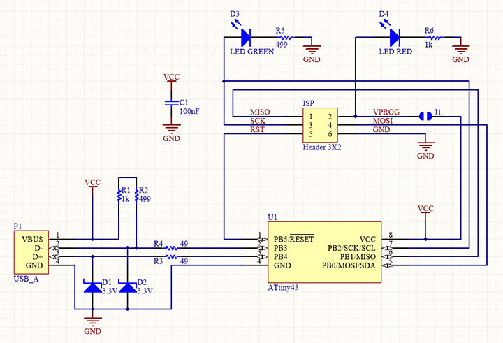
The schematic (PDF) is super simple: USB connector, ATtiny44, and 6-pin ISP header, with assorted passive components. I started with the Eagle files for the USBtinyISP,
although there's almost nothing left of it. Most of the parts for the FabISP are in the FabLab inventory.
Exceptions include the Mini-B USB connector (SparkFun, Digi-Key), 12 MHz crystal (Digi-Key), and 18 pF capacitors for the crystal (Digi-Key).
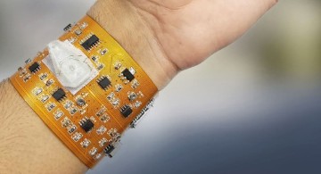
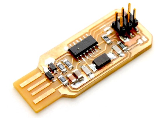
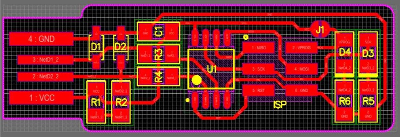
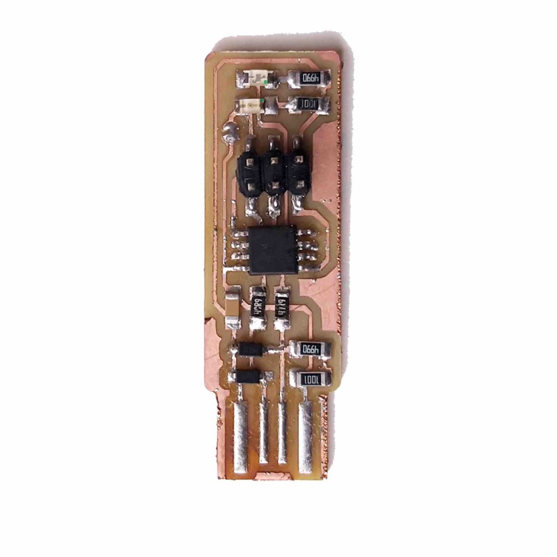
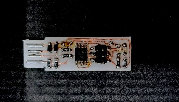
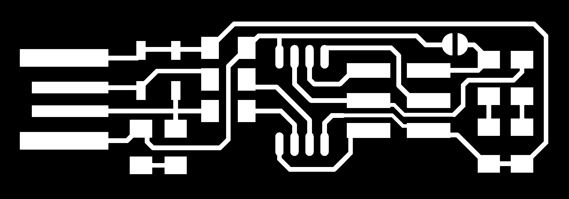
FabISP PCB is single layered PCB.
Making of FabISP
Milling process
First of all to make FabISP we need to mill the PCB.
Download (*FabISP board I milled was originally created by Brian.)
all files required to mill the board. You need trace.png and cut.png Which you can download from below.
Note: Milling resolution also depends on resolution of image. use high resolution image to mill.
We have Roland Modela RDX-20 in our lab. I used standard Fab ISP files as mentioned above.
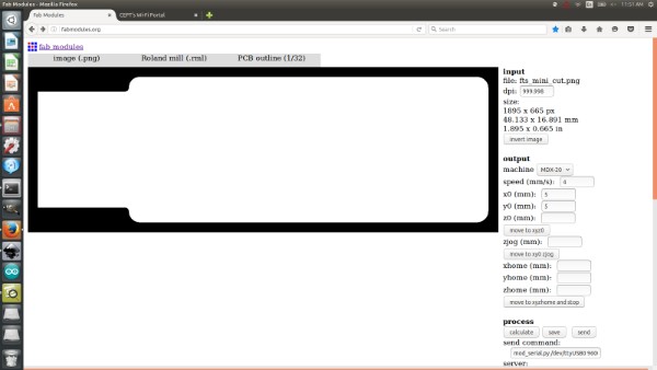
I milled the board using FabModules.org.
Physical Setup for MDX-20
Step 1 : Check if the bed is levelled. If not you need to lever it by putting Sacrificial Layer and by milling the board.
This takes up lot of time depending upon the size of the board.
Note: If its not levelled. Put the scarificail layer of wood or the board and mill it entirely to level it. This also won't ruin your bed while cutting copper.

Step 2 : After levelling. Put Copper board after applyinng DST (Double Sided Tape) on the back. Remove extra tape and put it on the left bottom corner of bed.
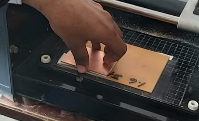
Step 3 : Set the bit according to resolution that you want. (1/64 inch for finer milling or 1/32 for medium resolution and use 1/16 for cutting ). Set Z axis of the machine so that bit just touches the copper layer.
FabModules and Generation of Toolpath
(Note for using Fab Modules for generating tool path go to this link.
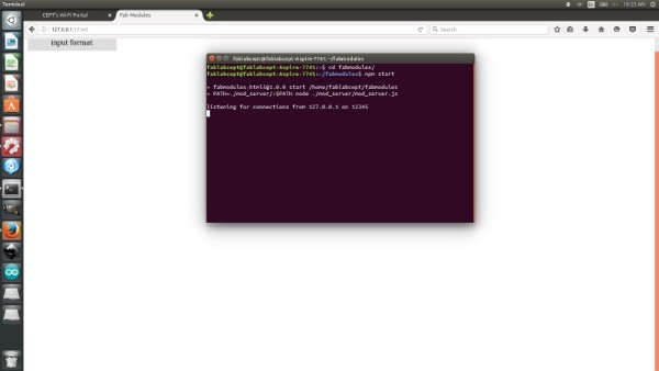
Step 1 : Go to terminal, FabModules directory and Write npm start. Now go to fab modes.
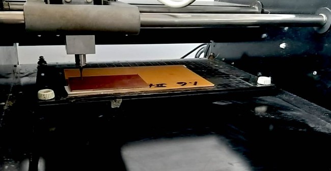
Step 2: Go to FabModules. Upload PNG image of trace path. Fill parameters as below. (Set appropiate origin.)

Step 3 : Make path and click send. It will trace and mill the path according to cut depth.
Important : x,y,zhome ddenots the co-ordinates of orgin. The speed is kept 4mm/s(default). If it is faster or slower it affects the performance of bit as bit rotates very fast. If its slow it will heat more and if faster it might break due to jerk. Set the correct tool diameter for the milling while generating .rml file.
Also From the group test it's understood that the minimum width the bit can clear is 0.016"(0.4mm) which is the diameter of the bit. The minimum trace is inconclusive as we had some difficulties in generating the right .rml file from FabModules.
1/64 bit is used for traces as it is thinner and helps to achieve milling for small components. 1/32 or 1/16 inch is used to cut the boundaries as we dont require minute path there. And 1/64 bit might break if its used for cutting.

Step 4 : See Roland MDX-20 doing its job.
Step 5 : Repeat same with cut file with larger (1/32 inch) bit with same origin. (Note: Cut depth will be more. Should be just enough to cut through the thickness of board.
For that measure the thickness of board prior to the begining of process)
Step 6 : Remove the board and clean it.
Soldering
This process requires precision and practice. (Try it on extra board and then do it on final)
Step 1 : Collect All Components as Below.
Refer Board Diagrams and Schematic and figure out what goes where.
Schematic
Board Diagram
Refer turorial on Soldering as below.
(Note : Be careful while soldering. Do not leave soldering head on table. )
Soldering Tools
Soldering Iron
Soldering Station
Tips
Wet Sponge
Iron Stand
Solder Wire
Helping Hand (Third Hand)

Trying to learn Soldering

Refer this amazing guide as below :
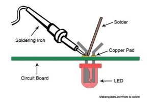
Step 1: Mount the component on board.
Step 2: Heat the joint
Step 3: Apply solder to joint ( Don’t touch the solder directly to the tip of the iron. You want the joint to be hot enough to melt the solder when it’s touched otherwise it will form a bad connection. )
Snip the leads.
Tips and Tricks

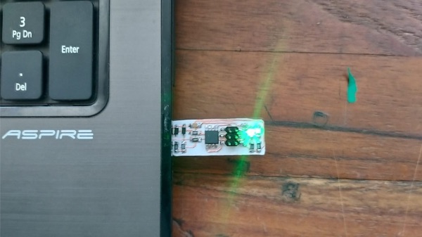
After soldering ISP would look like as given below :
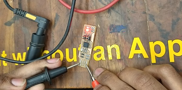
Testing
Once board is ready, test the connection with Multi-meter(in Buzzer Mode). It will beep once the connection is good.
For learning more about it go to liink below.
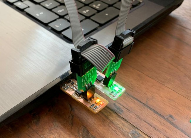
Programming the FabISP
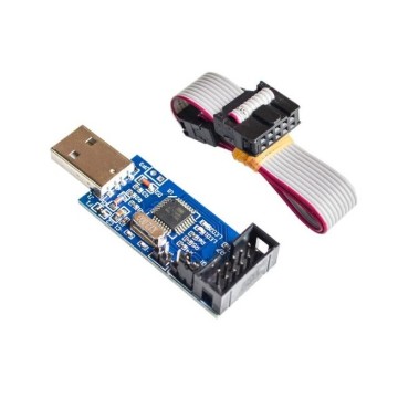
To program ISP, you need a functional programmer.
I used ATMEL AVR MK2 programmer to program as it was available at our lab.
Also I programed it using a linux system.
In all you'll need AVR MK2 programmer with 6 pin header converter and usb cable, linux based computer system, and Fab TinyISP board.
Step 1 : Install the firmware through terminal.
sudo apt install avrdude gcc-avr avr-libc make
Step 1 : Download source codes from below.
(*Note: Souce Code was downloaded from Brian's FabISP page.)

Step 2 : Go to the directory using ' cd ' command.
run 'make' command.
Update make file with name of the USB.
(you can do this by running gedit and opening makefile in the folder)
change it to avrisp2 to usbtiny.
(we are using AVR programmer)
make flash
make fuse
In case if you get errors run :
sudo dmesg
make fuse
Below is the AVR program installing guide.
Checking and Programming other ISP
Attempt with Vinyl
Contribution To Group Assignment
This week's group assignment was easy. I contributed into making of micro -milling tolerance test. (Ronald RDX -20).
Through this test I understood upto what distance the machine can cut traces properly. Thus we used smallest bit ie. 1/64 inch.
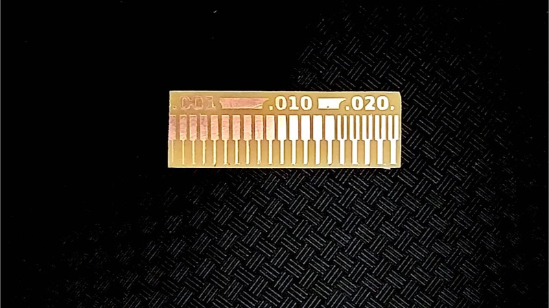
For detailed documentationn follow 'Group Assignment' Tab at the end of this page.
What Did I Learn?
This week was interesting, I learned about various components of PCB and what they do.
I also found out tricks of soldering and learned how to solder. (It was almost impossible for me to solder using soldering iron as my only left hand works. I took help of my classmates to solder. Then I turned to using Soldering Paste and it worked for me.)
Used terminals and managed directories using terminal for the first time. Also learned using mods.
