6 - Electronics Design
Group Assignment
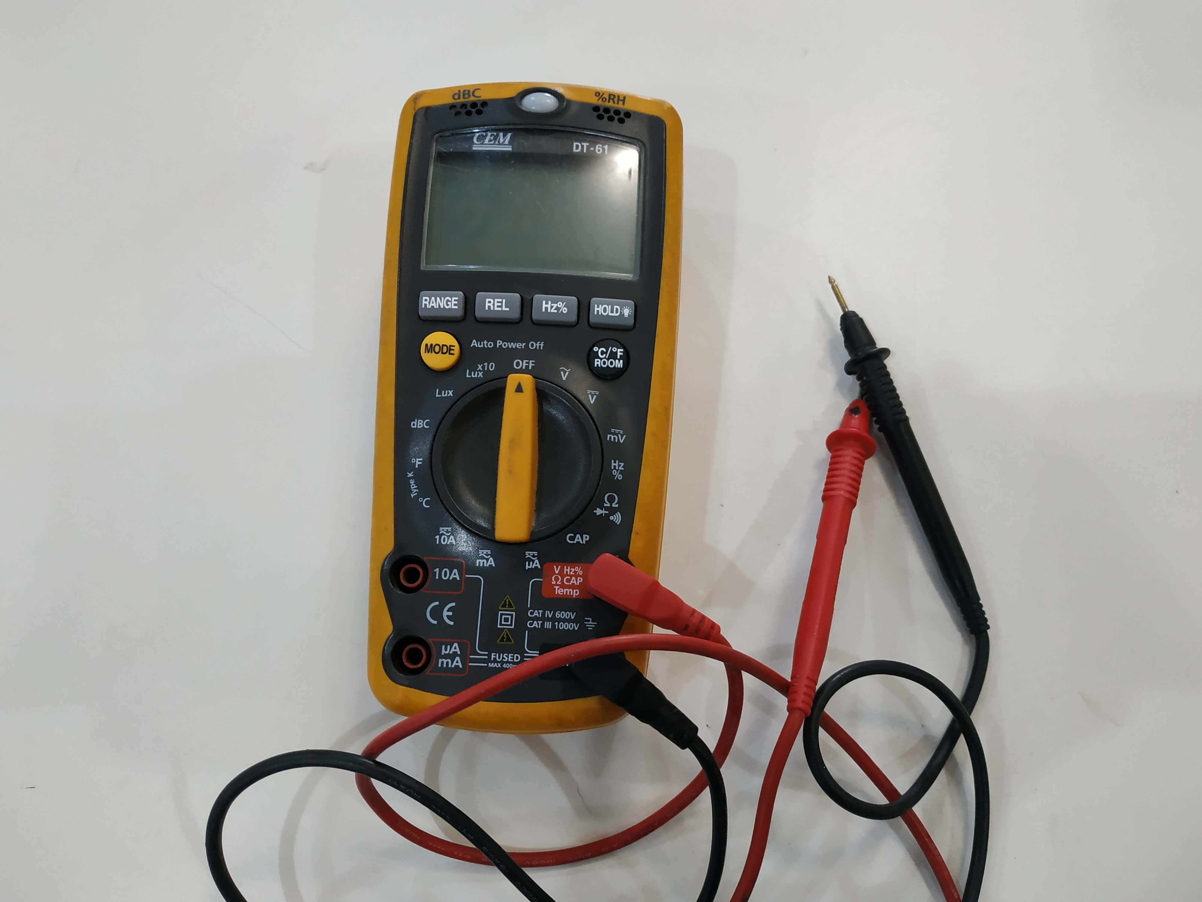
For this week assignment I used a lot the multimeter to check the connections before and after soldering to see if the routing was well done and check if there was any problem. I checked the VCC and ground connections first because it can burn the chip or the components. I did the error to not check all the connections, and then, programming the board, I realized there was a problem with the button connection.
Indiviual Assignment
For this week we had to design our first PCB, and it was a very interesting week. Two weeks ago we produced our first board, but designing it is much more complicated. The first step is to learn a design software. The instructors from FabLab Barcelona gave us a tutorial and a demonstration of how to use Eagle and Kicad. Eagle is maybe a little simpler, but Kicad is OpenSource and has very good features, so I decided to use Kicad.
Our starting point was the echo hello-world board and we had to add to it, at leats, a LED and a Button. I decided to go for it and add a RGB LED to learn more about this component and to do a different design. With that idea in my mind I opened Kicad and start the design.
The first step is to create a Project, it will be a folder where all the file will be saved. It is important to know that Kicad is the join of diffrent softwares working togther, one for the Schematic, one for the PSB design and much more. It has a lot of cool features. With the project created, we need to import the fab components libraries and the components footprints to get our design correct with our components. You can download the libraries from here. You can see this tutorial and see how it is done.
Schematic
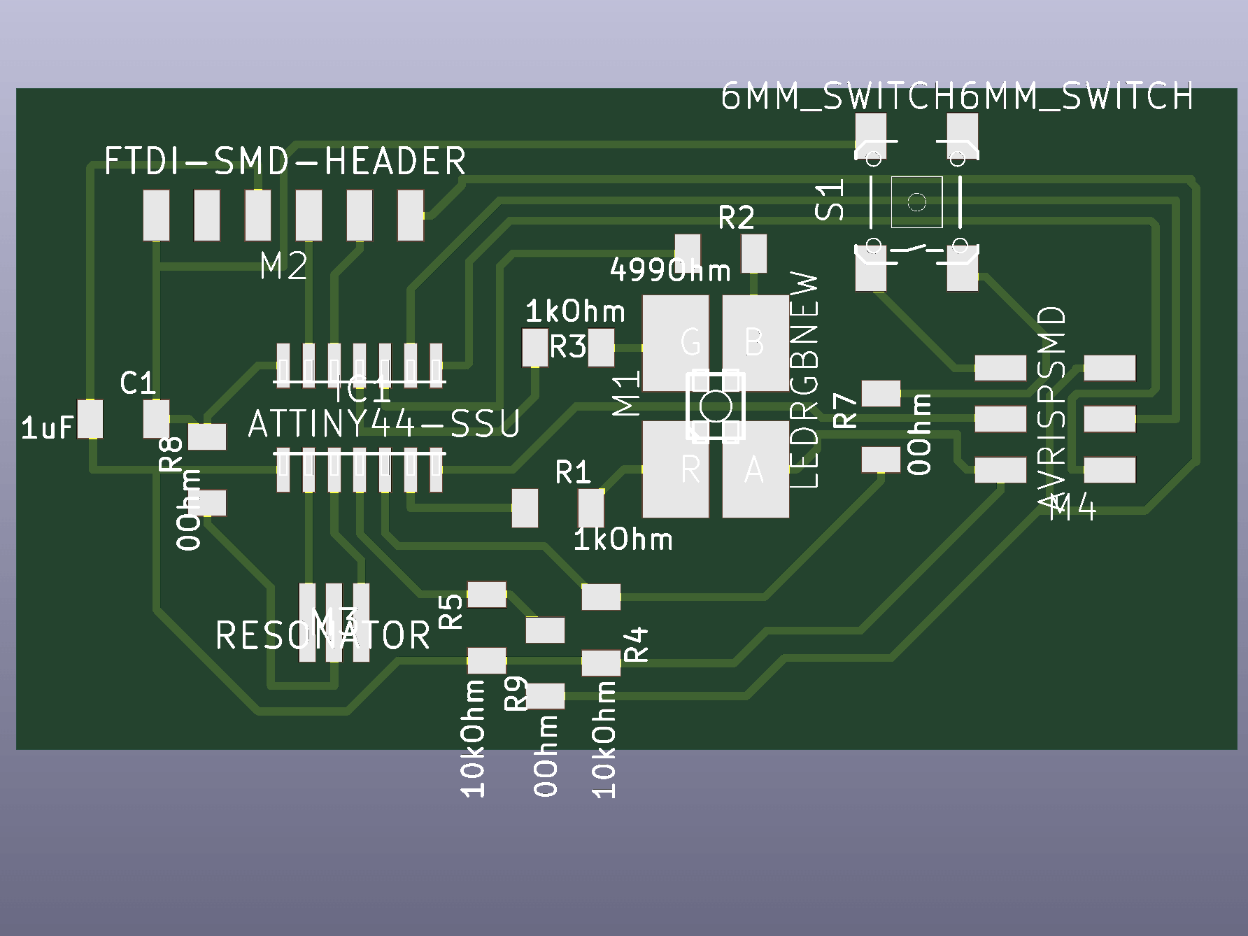
The first step is create the schematic of your board. This means adding all components that you need and define the connections between them. In my case I use the following components:
- Attiny-44
- 20 MHz Resonator
- 1uF Capacitor
- Switch
- RGB LED
- 499Ω Resistor (Blue LED)
- 1KΩ Resistor x2 (Red and Green LED)
- 10kΩ Resistor x2 (Pull-up resistors)
- 0Ω Resistor x3 (Jumpers for routing the board)
- 2x3 Pin ISP Connector
- 6 Pin FTDI Connector
As I wanted to use an RGB LED, I needed 3 different resistors for each LED, because inside the component there are 3 LED encapsulated. Looking to the datasheet, I saw that the resistor needed for the Blue LED is different than the others, because it needs more power to bright like the others so the resistance have to be smaller. Using a 499Ω resistor insted of the 1kΩ is the solution to it. Also, it is important to use pull-up resistors for the switch and for the Reset pins, to protect it from little currents or bouncing. This is the final result:
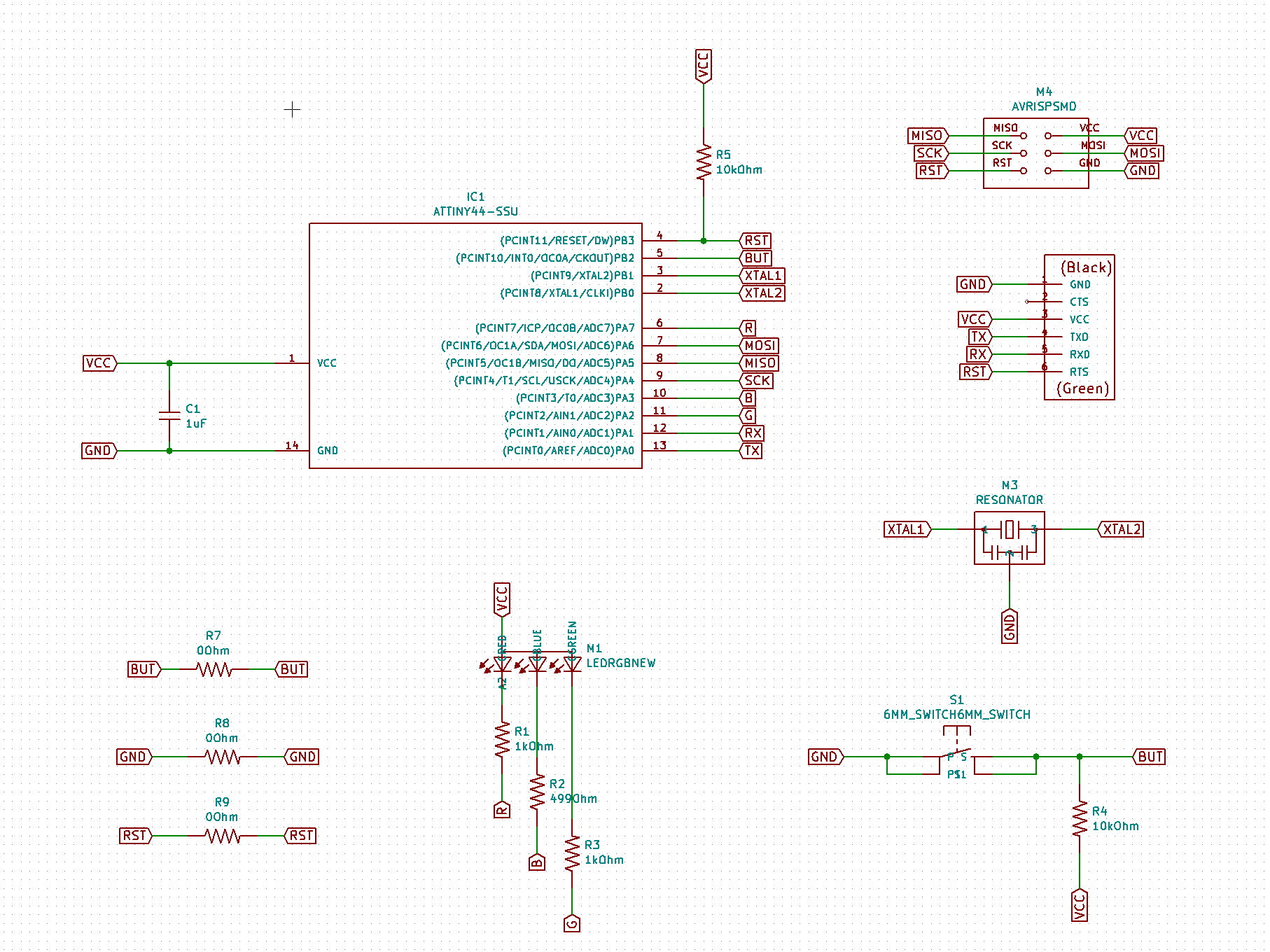
When you are done with the schematic, you have to generate a Net list with all the components and connections. This list will be used in the next step to create the routing.
Routing the board
With the schematic done, the next step is to route the board. To do it, we have to change to the PCB layout editor window in Kicad. Then import the Net list that you just created. Notice that you can allways go back to the schematic, but to load the changes to the layout editor you have to generate the Net list again and.
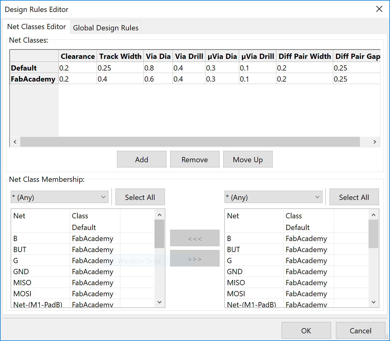
All component will appear and white lines show the connections between them. Now it is turn to organize all the components and create the routing. To make sure you are creating a route that can be milled afterwards, you have to change the Design Rules in the SetUp menu. These are the correct values:
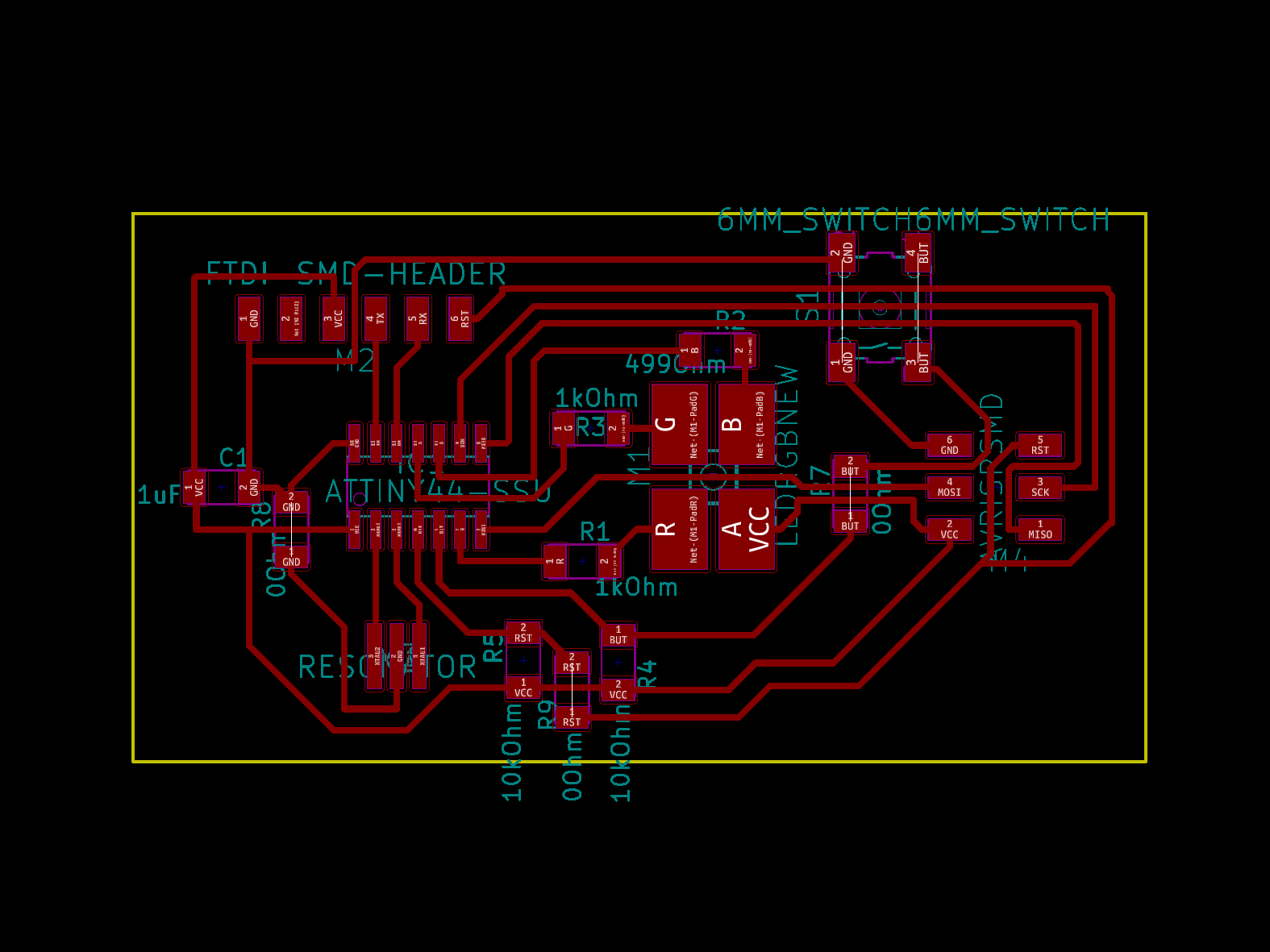
Creating the route can be very difficult, but there are some tricks. For example, after a long afternoon trying to route all the board (and that one is easy... it was my first time doing it) I decided to use 0Ω resistors as jumpers. This allows you to jump over a connection without mixing them. This is the final result.
3D Model
Before soldering, it is important to know where all the components have to be placed, so I extracted a 3D model from Kicad, and here you can see the exact position of all the components, it is very helpful.
Milling the board
Now it is time to mill the board! This time I decided to use the Rolland MDX-20. That was easy, I exported the traces images from Kicad, then in Inkscape I separate the outline cuts from the traces exporting 2 PNG's and bring them to Mods as we saw on Week 04. Then pass it to the machine and mill it! First the traces with the 1/64 inches mill and then with the 1/32 inches.
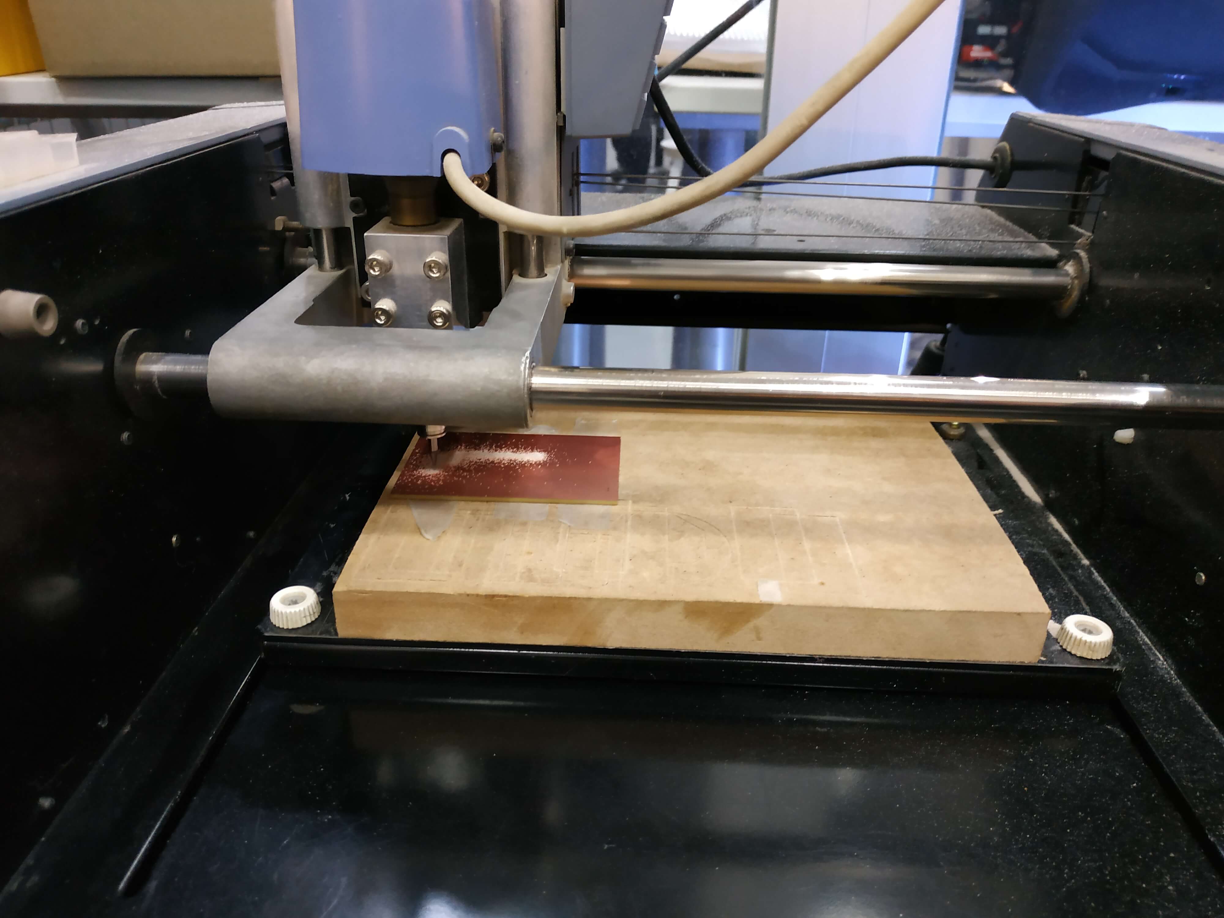
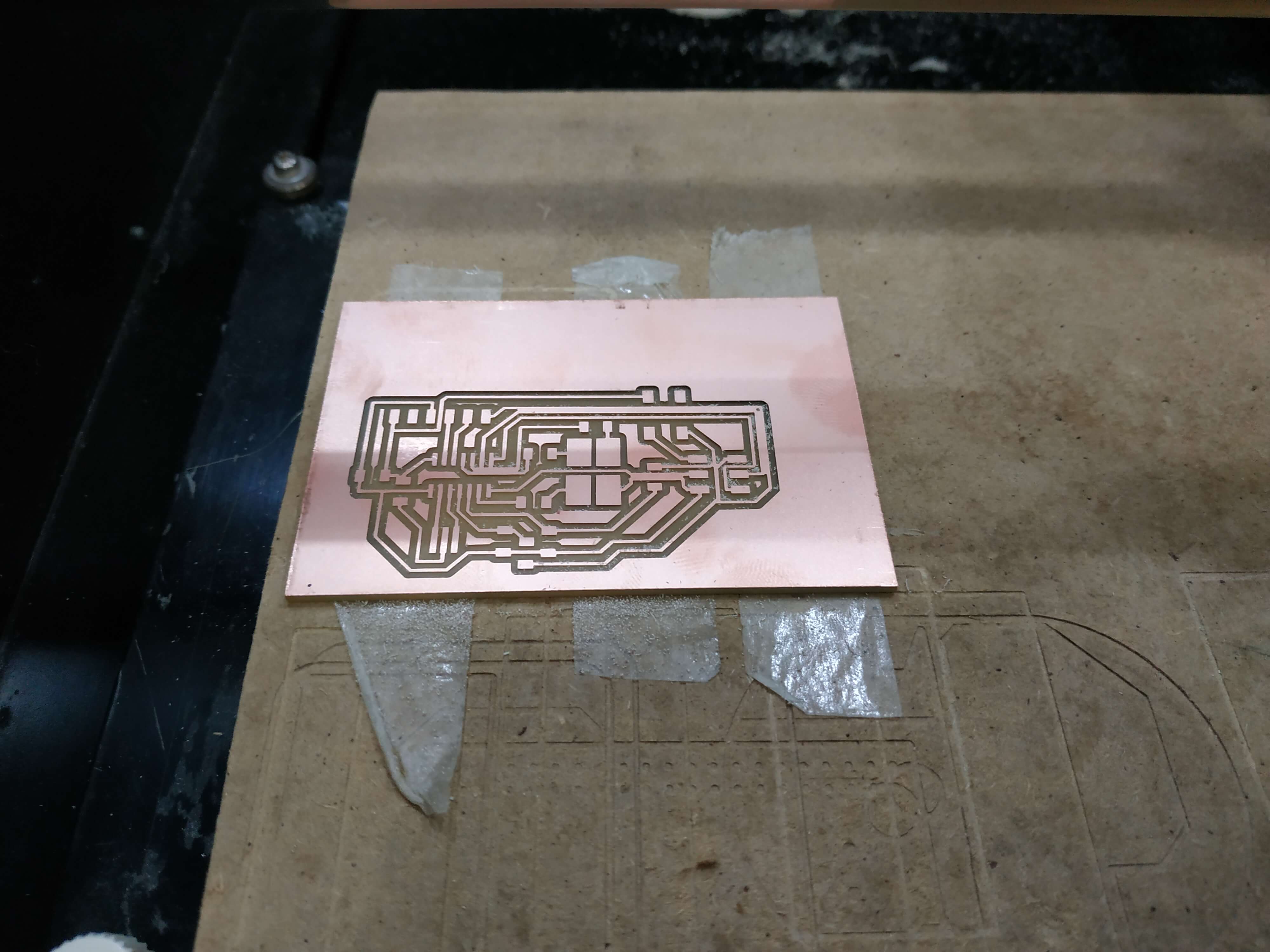
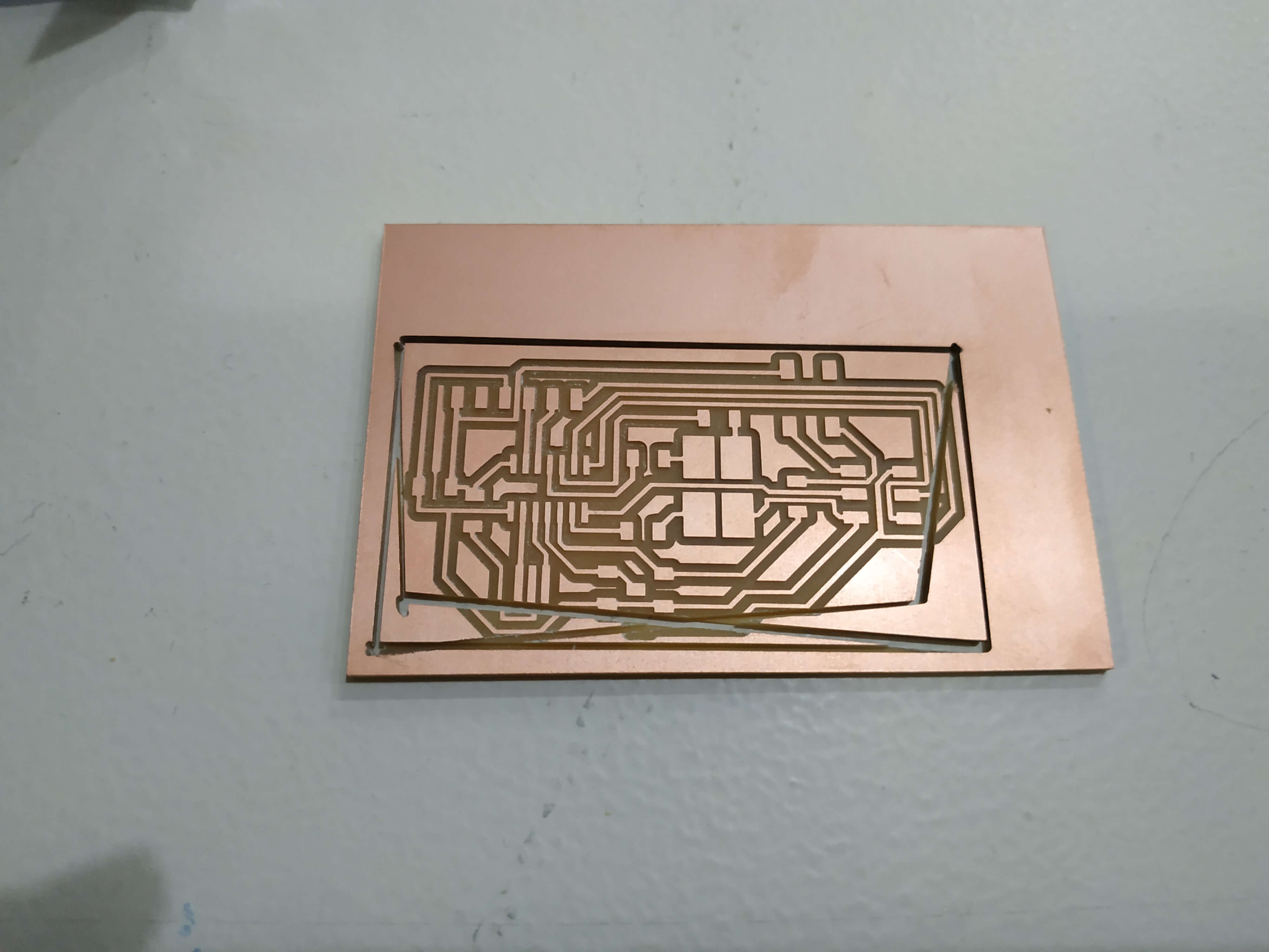
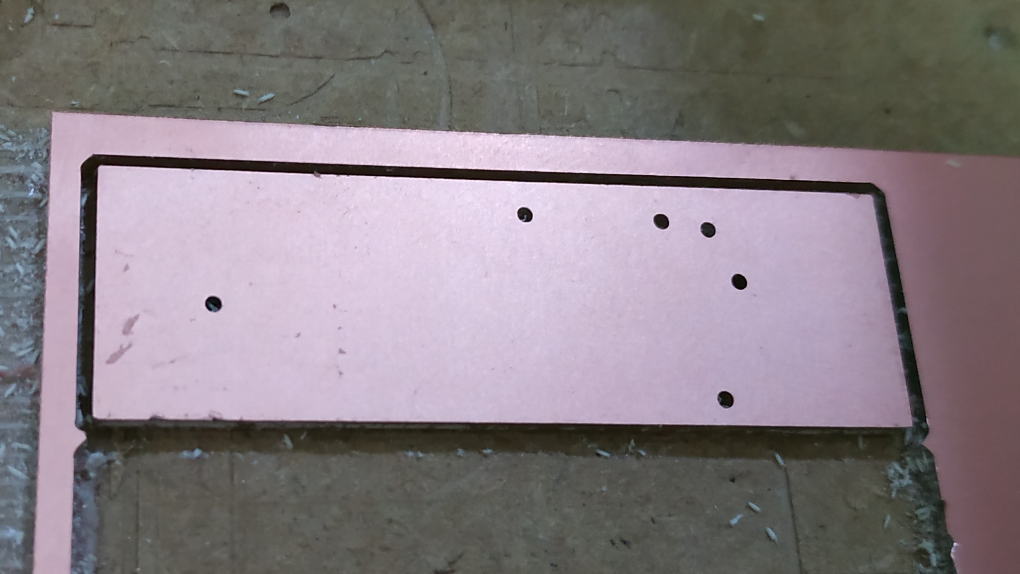
Milling the board was the most complicated part of the proces because I found some errors. The first one, as you can see in the first image I get a problem with the connections in Kicad as there were really close and the milling machine didn't go througth them, so I try to separate them with a cutter, but it was not working.
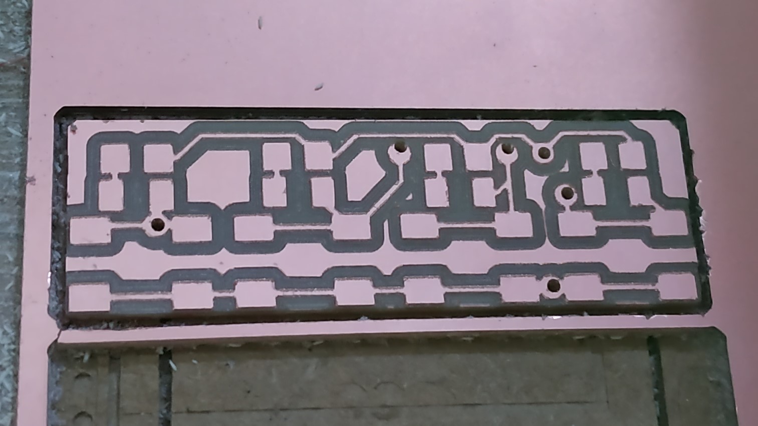
Then, after fixing the layout, I tried to do 2 round holes in the corners, but the software of the machine had a bug and after doing the outline, it doesn't read all the gcode lines and cut my board like you can see in the second image. Eduardo Chamorro fixed the problem increassing the wait time between reading commands, and finally I get the correct board.
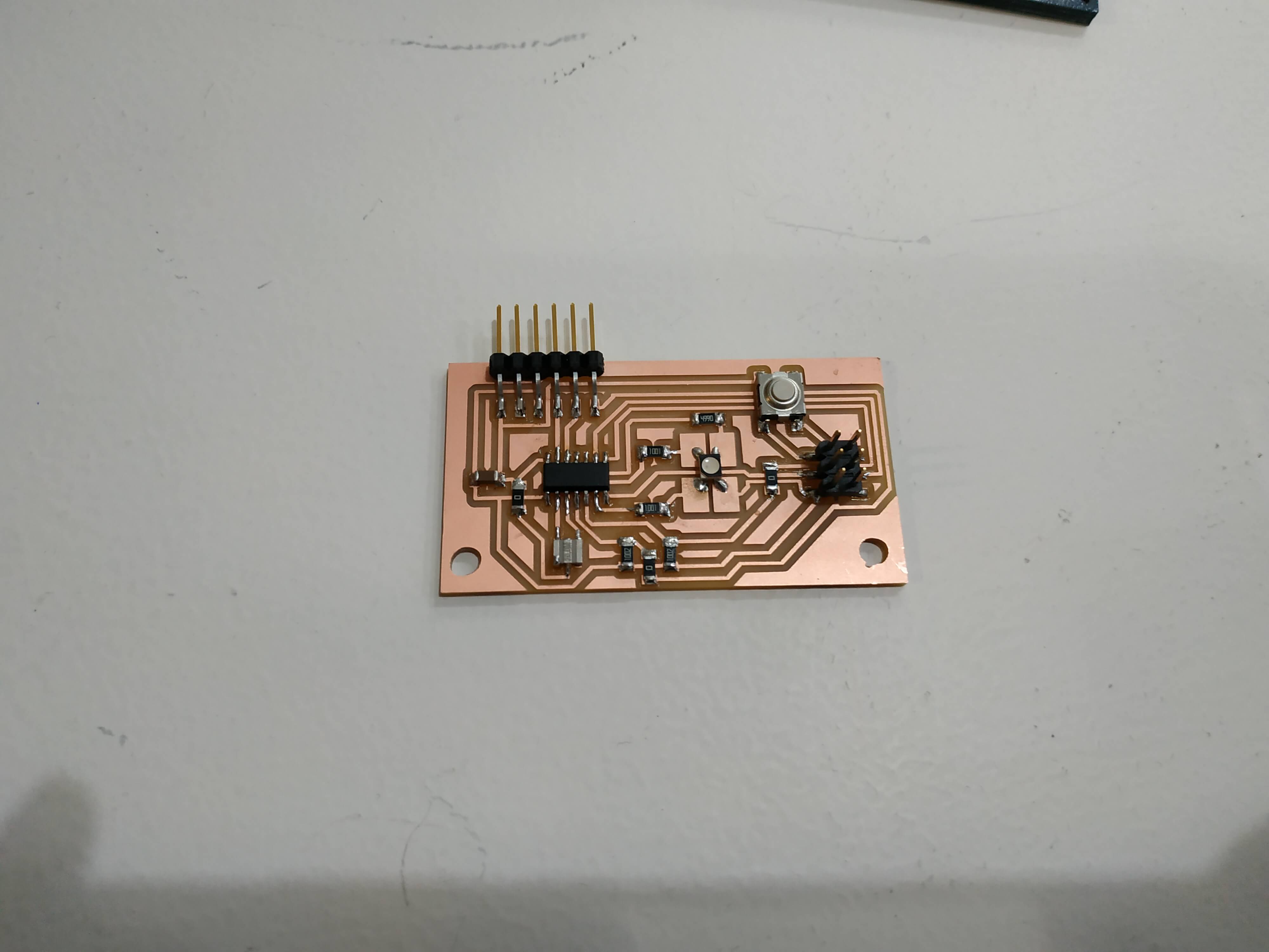
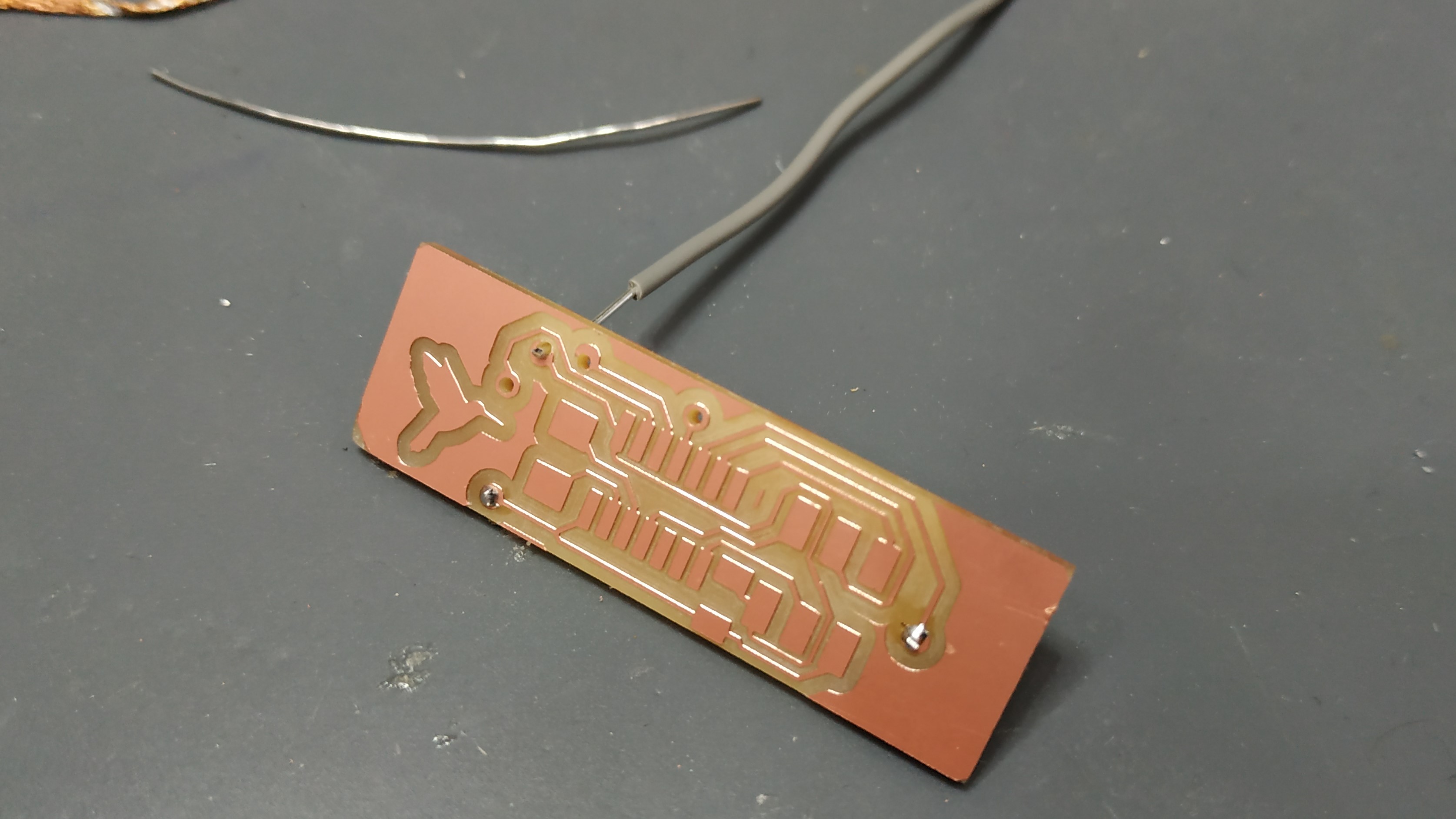
Soldering
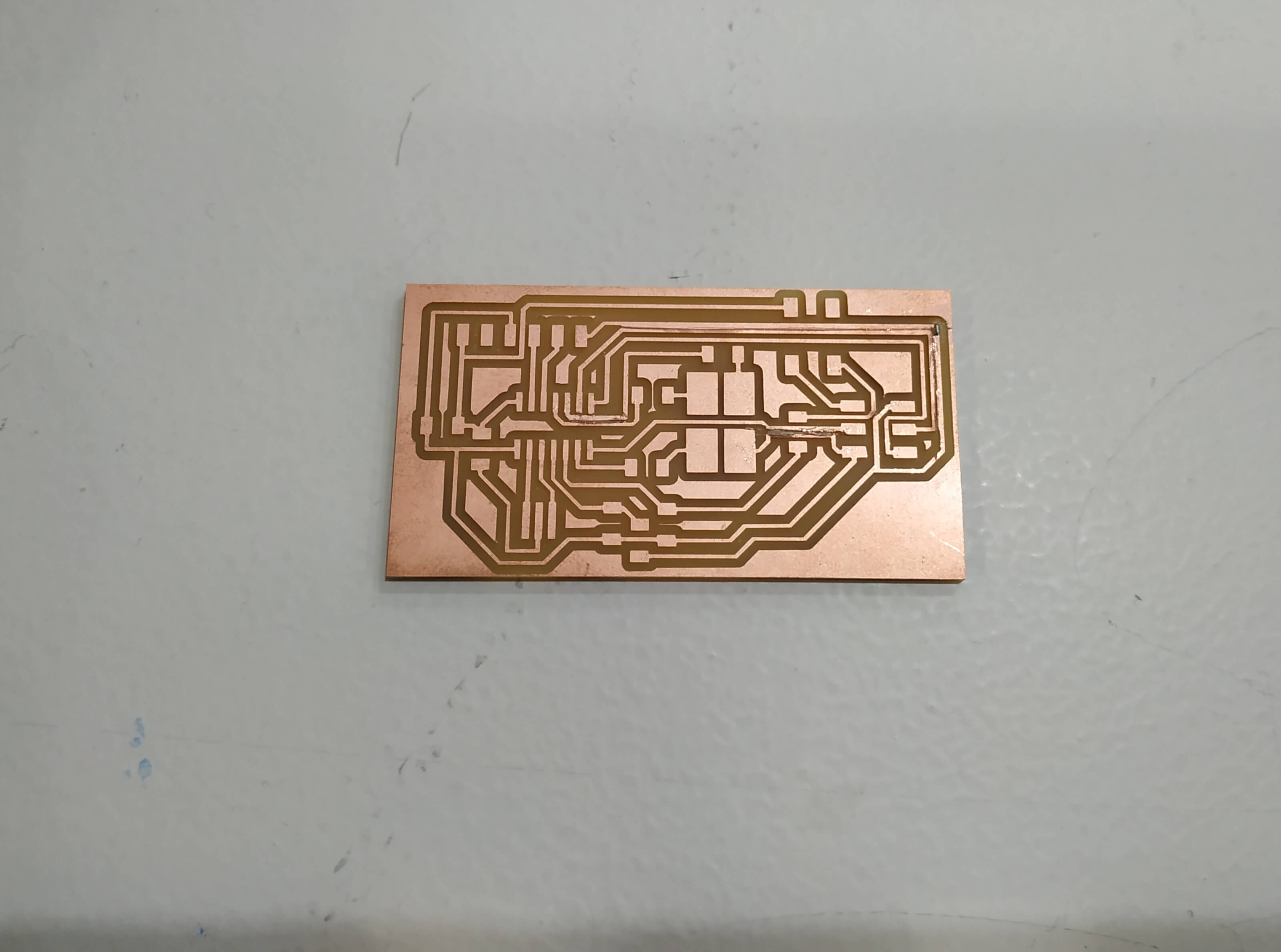
After week 4, soldering was easy and fun. I realy enjoyed it, put some music on and solder a board is the best part of the week. I had to solder the button and the ISP connection two times because when I was programming there was a problem with the connection with the button and it was a thin piece of copper between two pins of the ISP connection.
To detect the problem I had with the button, I did some troubleshooting with the mltimeter to make sure all the connections where right. Fatsly I detect that all the pins of the button where connected, so I decided to check the traces. There was no errors, so I tought it should be a problem with the soldering. I usold the button, but there was anything strange, so I saw that the problem must be underneath the ATtiny, and it was there. It was a small copper bridge between two connections. I realized then that I didn't clean the board before soldering, if I have done that before I am sure it would not have happened. Life lesson, cleane the board and check connections before soldering.
Programing the board
This part is better documented on week 8 - Embedded Programing, this is just a quick resume.
The final step was to program the board. To do it, I used the ISP programmer created during week 4. I program it using the Arduino IDE, because I am used to it and I know how to use it. To work with the Attiny processors I had to download the libraries. To do it you only have to follow this tutorial.
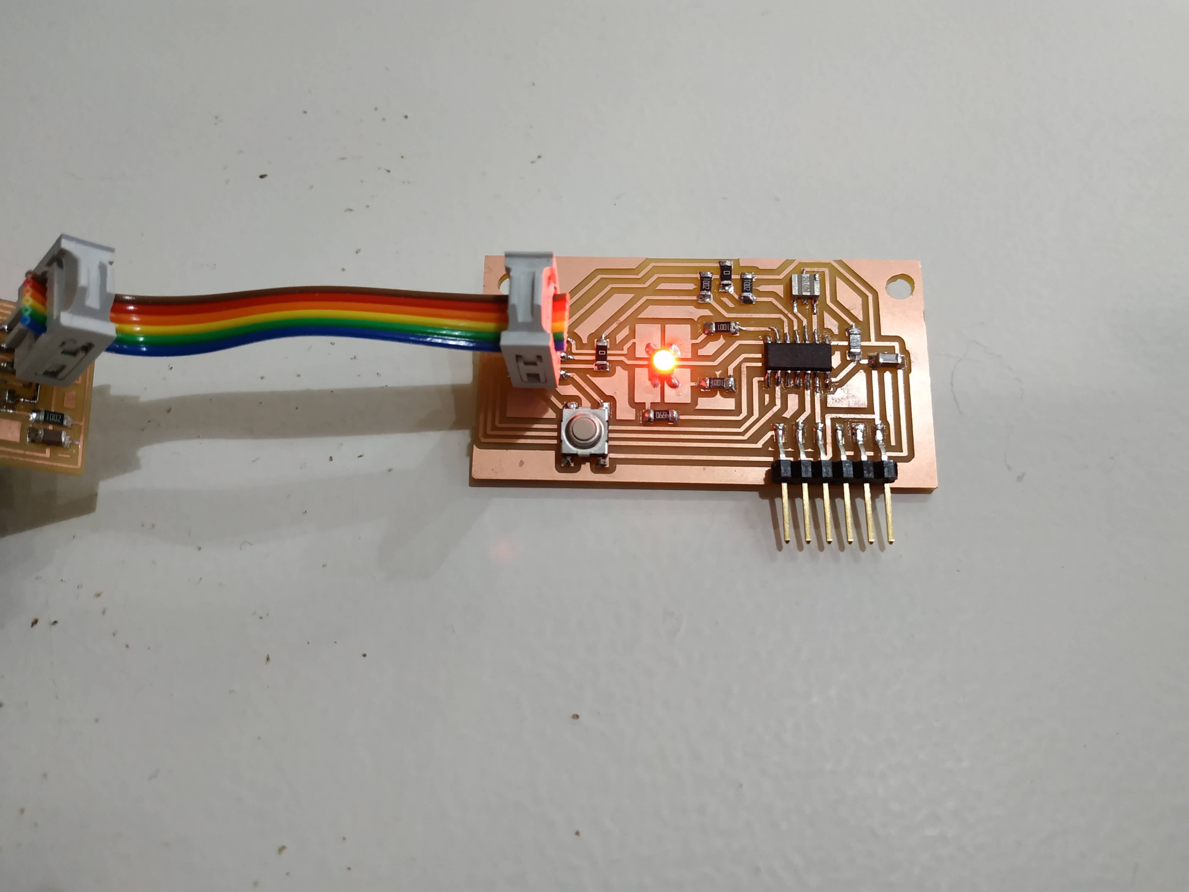
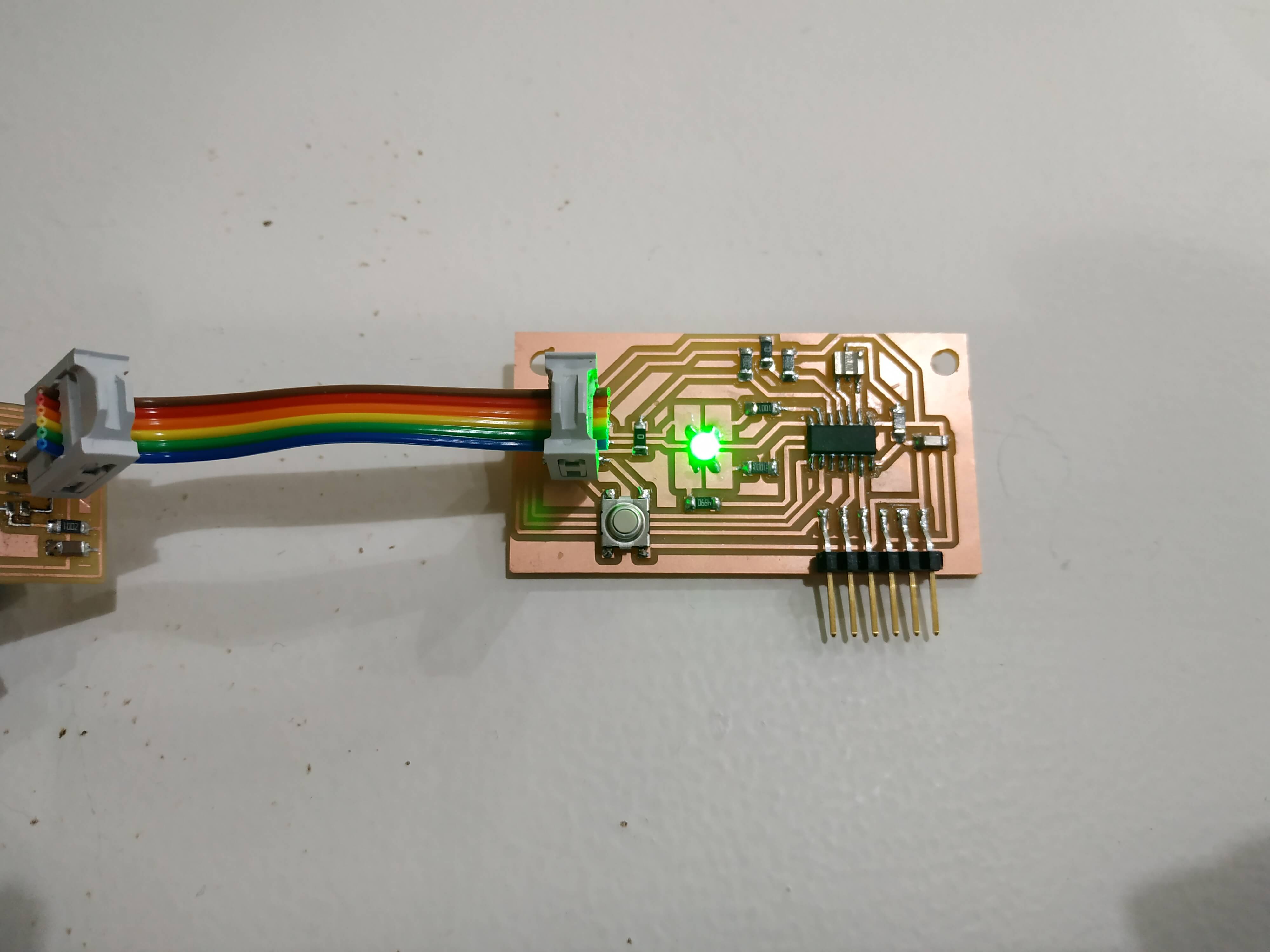
I did a simple code where the LED will shine Green when the button is not pressed and change to Red when you press the button. Here is the code:
int R=7;
int G=2;
int B=3;
int but=8;
int ButtonState=0;
int PushCounter=0;
int lastButtonState=0;
void setup() {
pinMode(R,OUTPUT);
pinMode(G,OUTPUT);
pinMode(B,OUTPUT);
pinMode(but,INPUT);
}
void loop() {
if (digitalRead(but)== HIGH) {
analogWrite(R,255);
analogWrite(G,0);
analogWrite(B,255);
} else {
analogWrite(R,0);
analogWrite(G,255);
analogWrite(B,255);
}
delay(50);
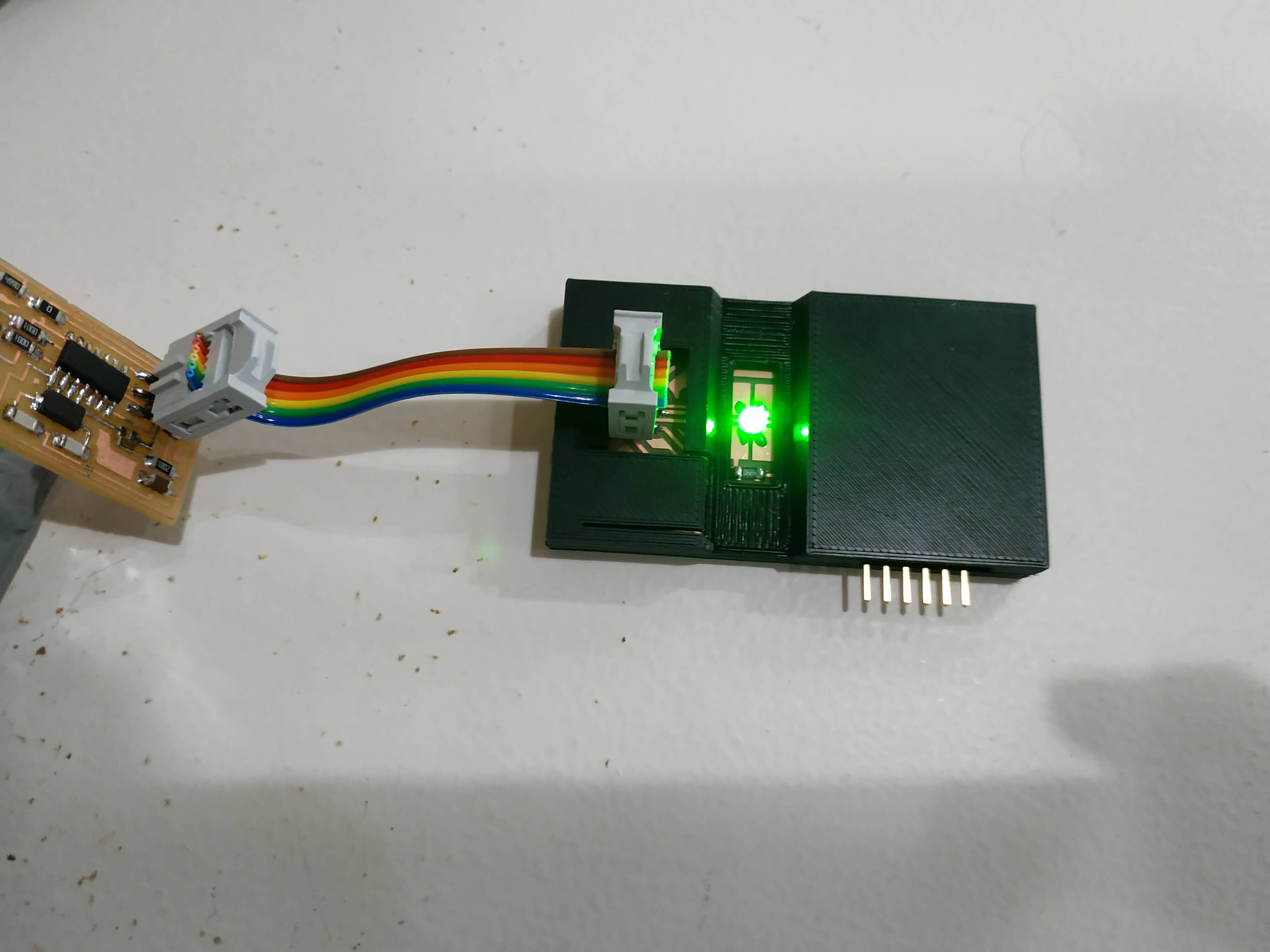
}Here are the photos of the LED with different colours:
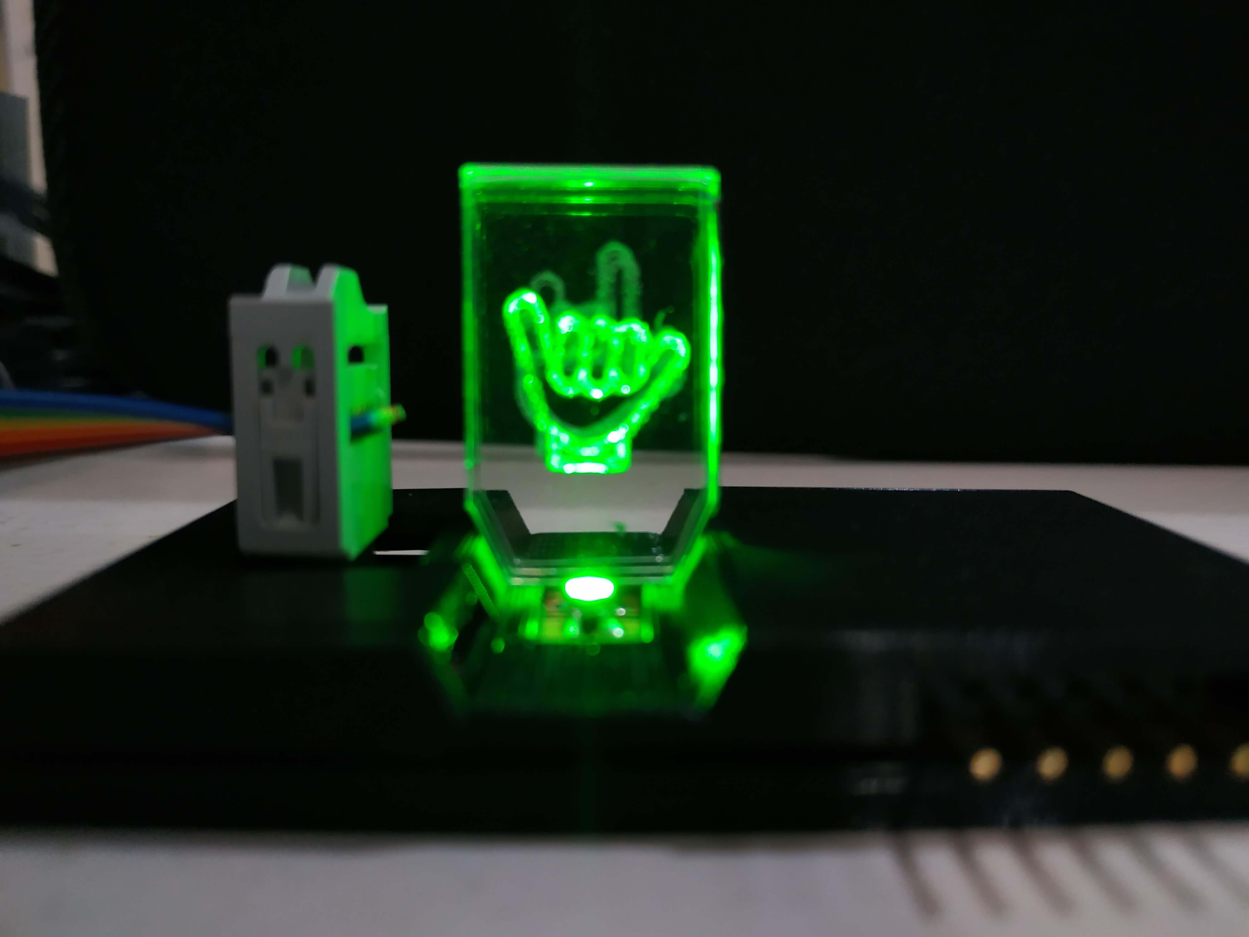
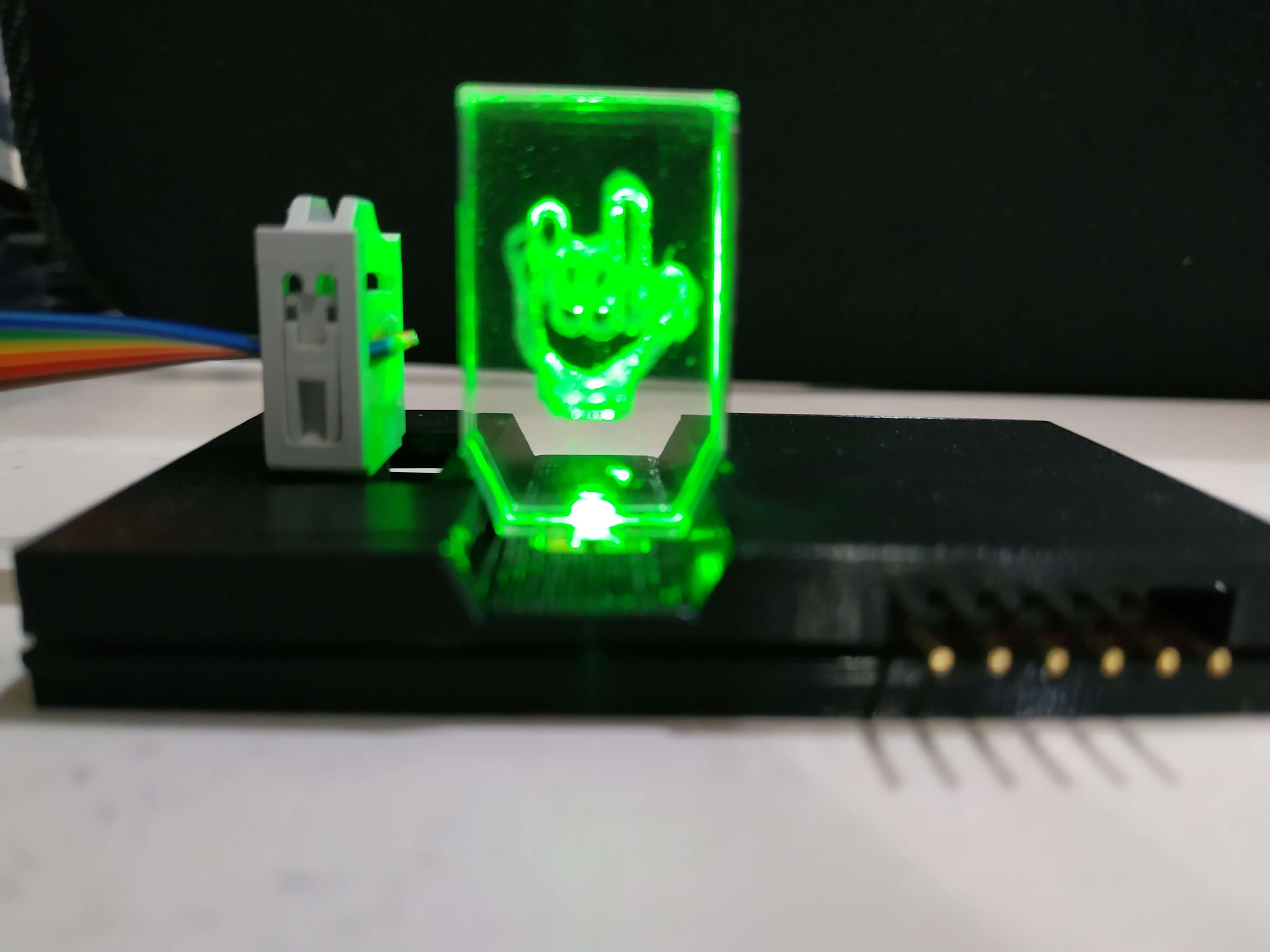
3D Case
With the assignment done I decided to do a 3D printed case for the board and use it as a light for an animation. The idea is to shine diffferent Acrylic layers with an image engraved on it. I did the design in Fusion 360, and this is the result:
Acrylic lighting
To design the acrylic layers I used Inkscape and then engrave the images with the laser cutter having this funny and amazing result. I will keep working on it to get a better animation.
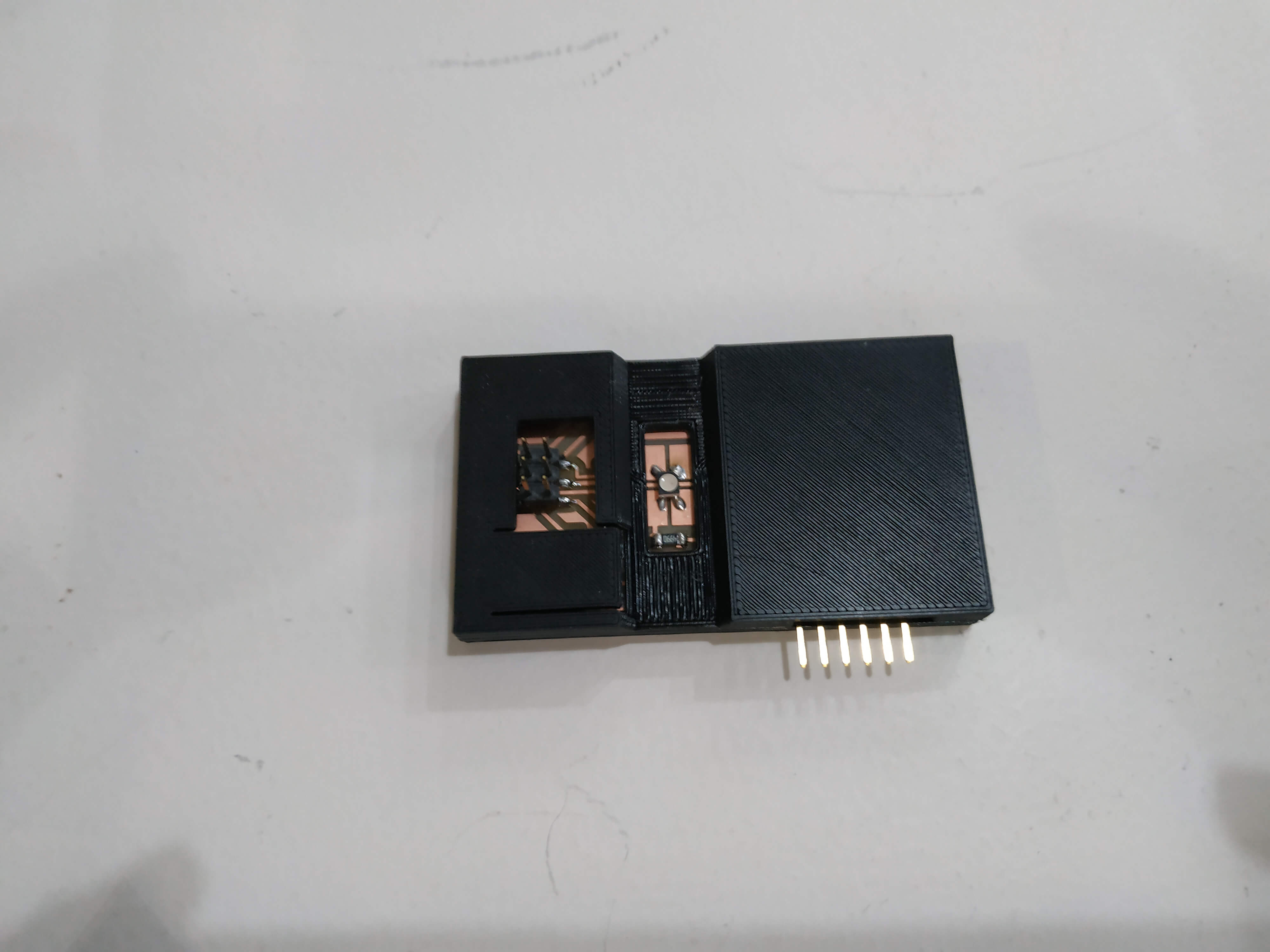
Two side milling
During week 13 - Networking and communication I decided to mill a 2 side board because I needed a small board. It was a complex process, but I manage to do it. I decided to document it here.
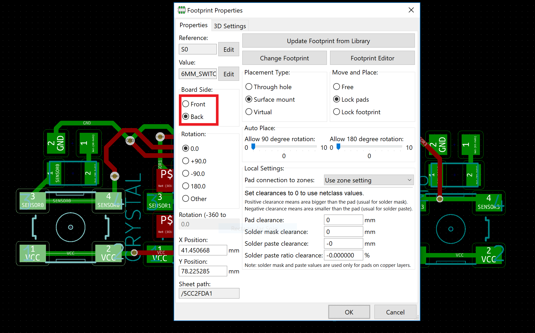
It is really easy to design the two sides of the board in KiCad, you only need to select the element that you want to place in the back layer, right clik and select properties. There is an option to select Front or Back. If you select back, you will see that it turns green and it mirrors the footprint as it is in the other side of the board. This is correct and you will have to think about it later. Here is an image of the properties menu:
With the design done, the next step is to import it to SVG and create the PNG images with Inkscape. Note that it is necessary to mirror the back side to have the correct paths, I did the mistake of mirroring the front part and then I realized that I had the footprints wrong, I couldn't solder the ATtiny44, it needed to be fliped.
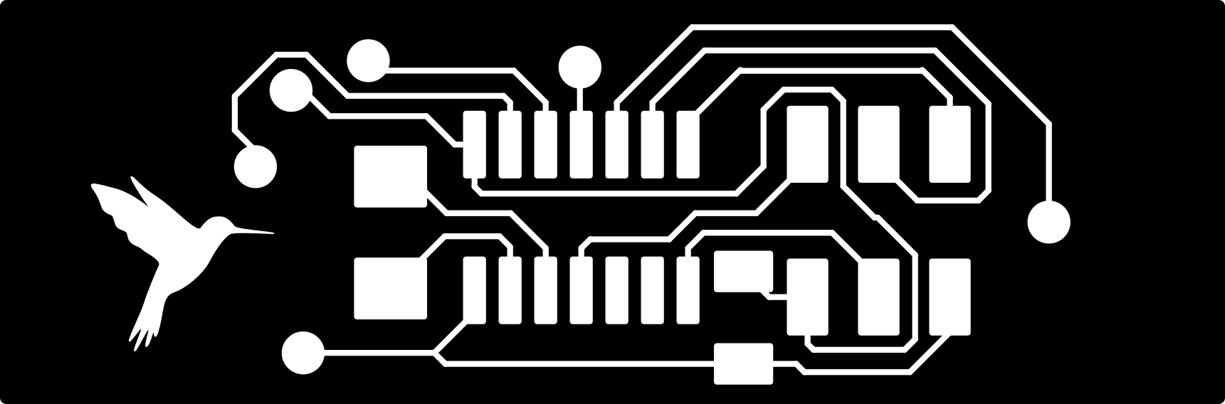
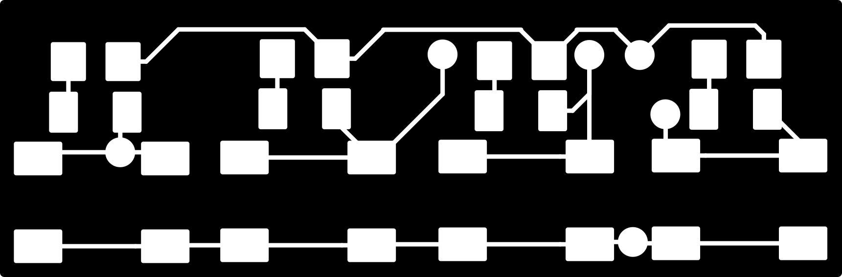
Also, I recomend to make the footprint for the holes bigger, so you if the board moves a little bit when you flip it it the holes have some area to move without destroying the board. Those are the four images you will need, the front part, the holes, the outline and the back part:


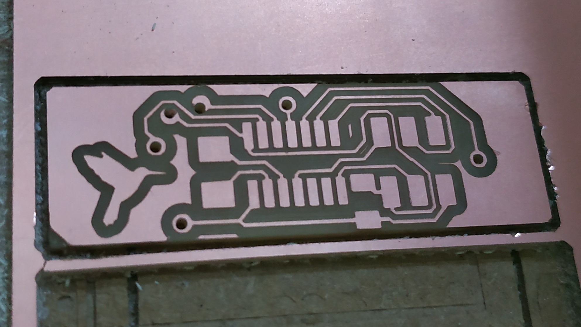
I thought that milling it would be the most difficult part, but it is not that difficult, in fact it is really easy to do. First you need to mill the front side. Then change the mill for the 1/32' and mill the holes and the outline like a normal board. Then, remove carefully the board, but do not remove the big board, only the milled part. Then you will have the space to put your board again. Flip the board, note that if you mirrored the PNG verticaly you will need to flip it vertically, if you do it horizontaly flip it horizontaly. To check if you have it right, you can compare the holes with your image, if they are OK stick it to the sacrificial plate. I recommend using a strong 2 side tape to ensure that it doesn't move with the vibrations of the machine. Try to center it as better as you can with the hole it left, small errors are solved with a bigger hole path, thats the reason why we did it before. Then mill the back part and you will have your board.
Finally, to solder the 2 sides together, I decided to use some wire, solde one side, solder the other and cutting the wire. Be very carefull when you solder the second side, to don't unsolder the first one as the iron will heat the wire and melt the solder.
Conclusions
This is a very important week because all final projects had some electronics on it, so it is important to learn how to design a board and route it. I also enjoy it a lot because I really like electronics and I had fun doing it and soldering the board.