Week 7: Electronics Design
Group project:
Use the test equipment in your lab to observe the operation of a microcontroller circuit board.
Individual project:
Redraw the echo hello-world board, add (at least) a button and LED (with current-limiting resistor),check the design rules, make it, and test it.
Extra credit: measure its operation.
Extra extra credit: simulate its operation.
We got a nice start as in the lecture we went through what components were needed and how to make schematics. First we started a new project from File > New > New Project and named it week7. Then create new schematic, either from menus again with File > New > New schematics or by right clicking newly created project and choosing New > Schematic.
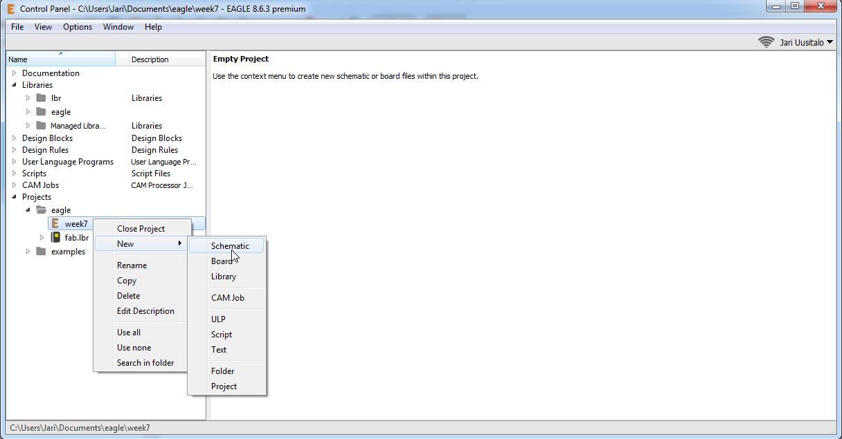
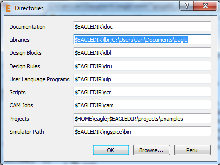
Downloaded a fab.lbr component library, put it under /documents/eagle and added that path to Options > Directories.
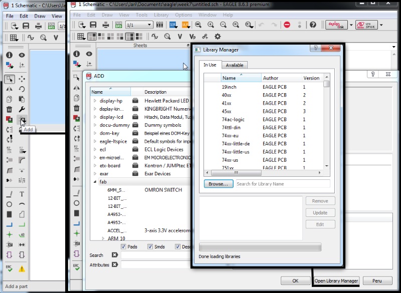
Checking if the fab component library is in use, by opening the Library manager(From Add > Open Library manager) and typing the name of the library in the search field after browse button. If it is not in use, click browse, find the library(where you put it after download) and open it.
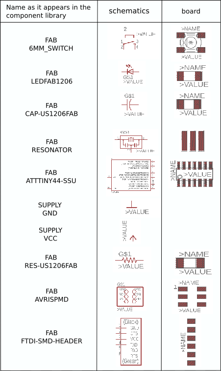
This is the list of components needed for the board. VCC and GND were the only ones outside fab component library and were found inside supply category instead.
Added all the components listed with Add tool, some resistors multiple times. Then it was time to draw some lines, using the Net tool. Green lines crossing over are connected ONLY if there is a green dot in the crossing. Finally added values by right clicking the component and choosing value option from the list. Components included in the button section are there for improved push button debouncing, as instructed by Antti.
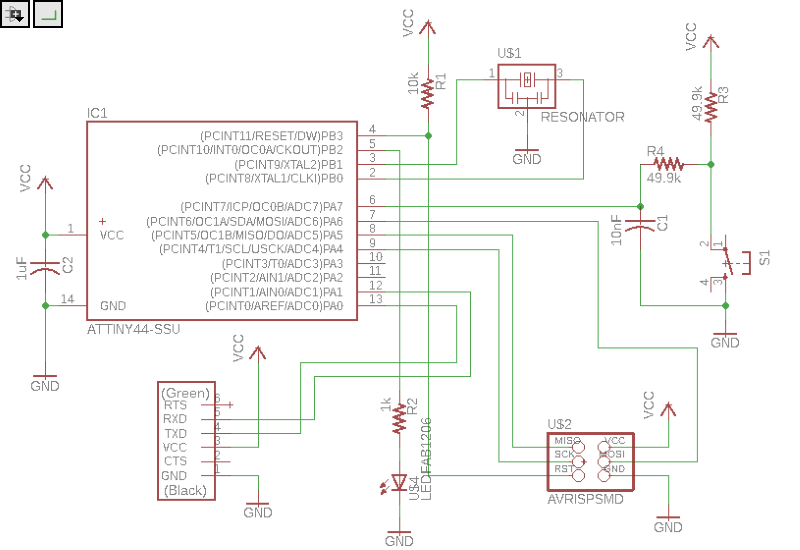
With schematics ready, it was time to Generate/switch to board design.
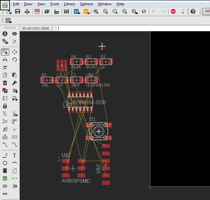
Moving and spreading the components, by clicking on white plus on components(selecting it) and then choosing Move icon(four small arrows pointing different directions), trying to make building the board possible.
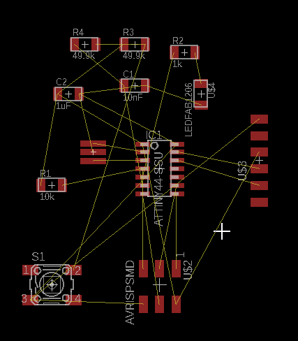
Finally I was satisfied with the component placement.
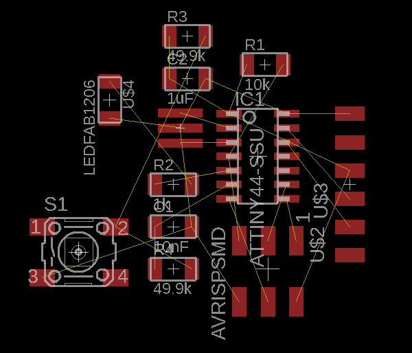
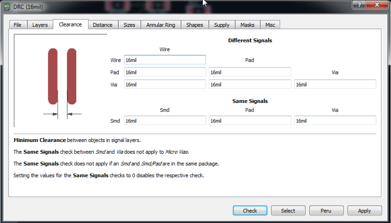
Added design rules for routing. Using 16mil as suggested.
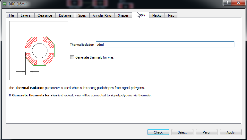
One more rule to add; From Supply > Thermal isolation: 16 mil.
Started to do routing by hand, by using the Route button.
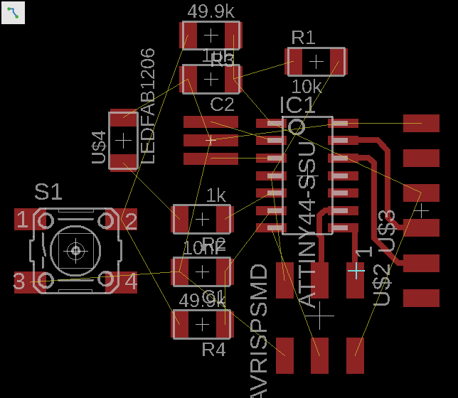
At this point I still didnt know there was autoroute command...
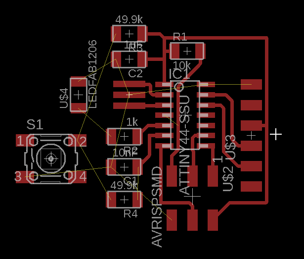
Routing finished. Or so I thought. One more airwire to connect.
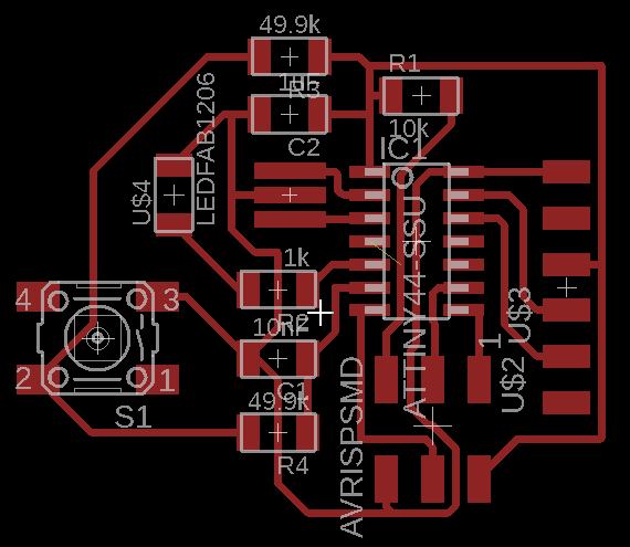
Adding ground plate by using Polygon tool, which creates dotted lines and joins them when drawing last line to starting point. Right clicking on the polygon gives different options and by choosing Name, I can name it GND.
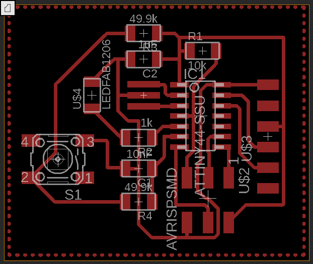
Hitting Ratsnest button now connects all grounds and makes the actual ground plate.
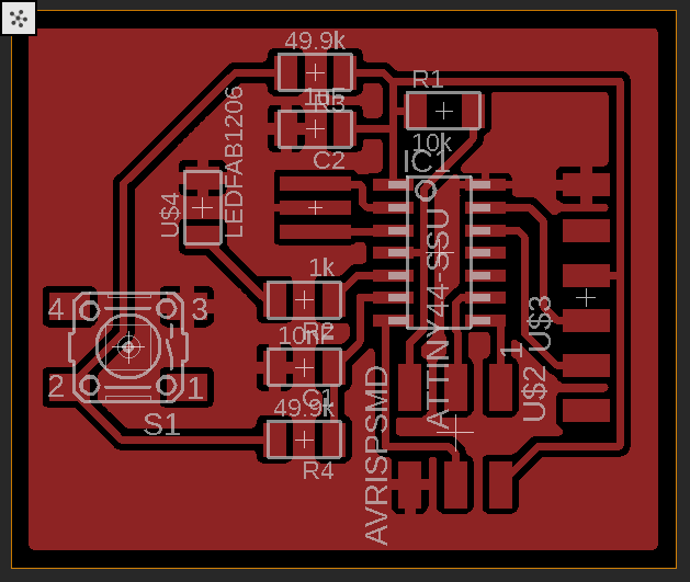
Finally, adding milling border, by using Line tool and setting line width to 40. Then changing layer from Top(1) to Milling(46) and draw blue lines to the board edges. When exporting milling images, use layers to select only top-layer for traces and only milling-layer for outline.
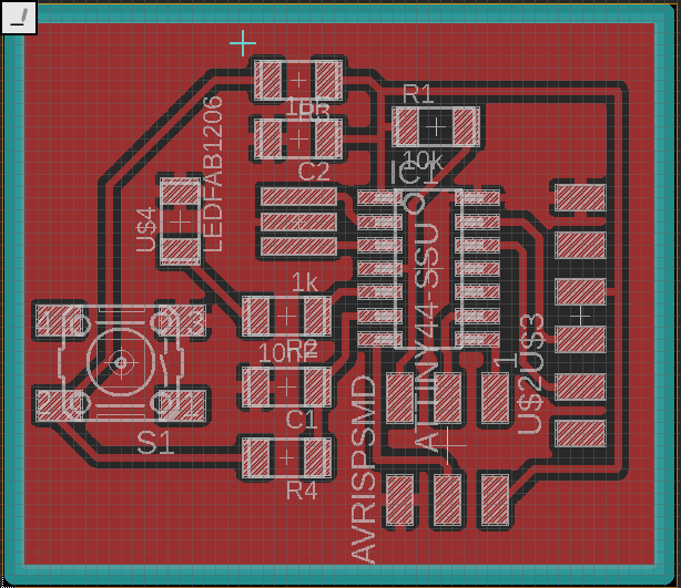
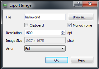
Export board as image. Check Monochrome for black and white image and changed resolution to 1500(Later on I used 1900 and eventually even 2400 as resolution).
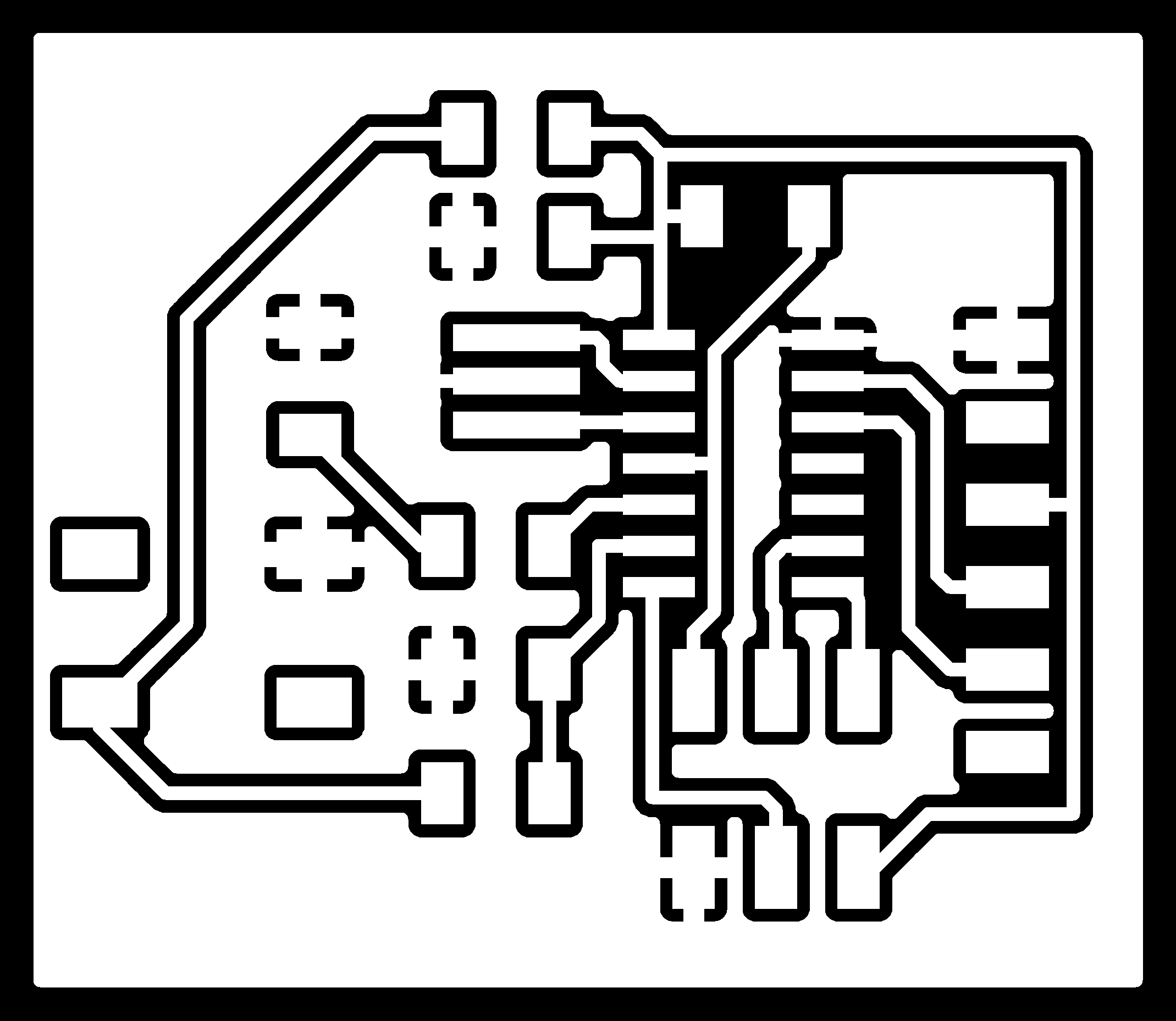
And the result of export.
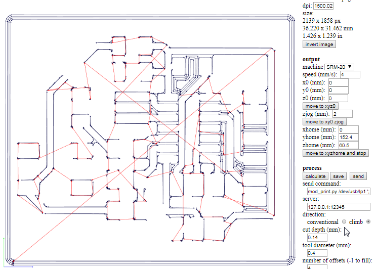
Calculations for milling failed when done like previously, 0.14 mm for depth and 0.4 mm for diameter. Later this was discovered to be because of the resolution and dpi value of the image.
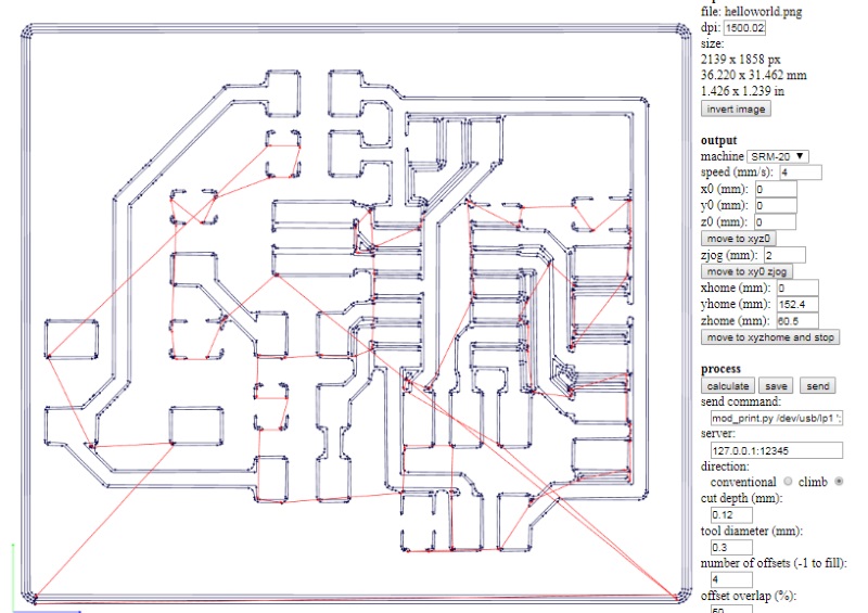
Now the lines look better with 0.3 mm tool diameter.
So milled my board and went collecting components from our lab's storage. After that scrubbed the board to remove photo sensitive layer and soldered everything in one go. This process was exactly the same as done in week 5 - Electronics production.
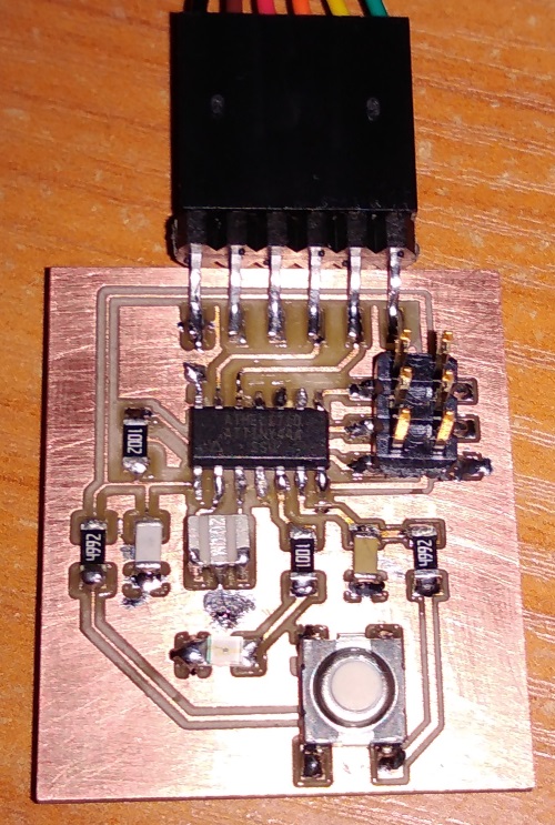
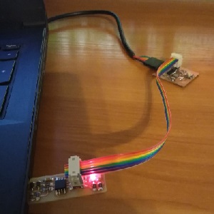
Setup my boards for programming. Used USB/FTDI cable to connect the new board and ISP cable between the boards. Check, double check and triple check the orientation of the cable between the boards, because this was giving me a headache.
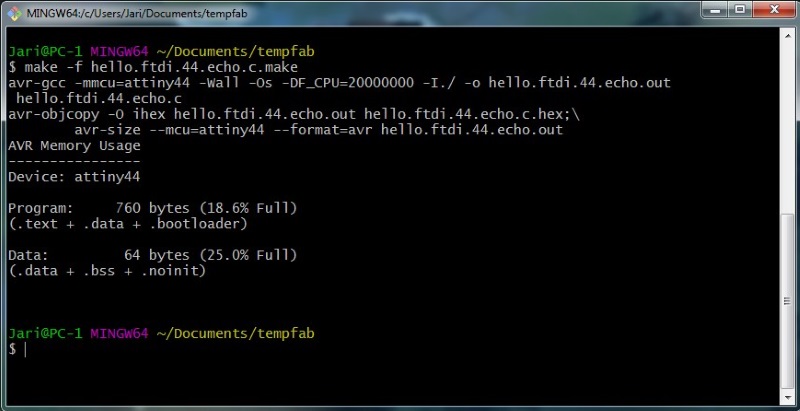
Now I needed to make a .hex file for flashing, so I downloaded code and make files, and run the command;
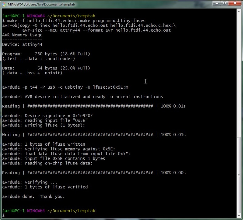
Setting fuses to make the board ready with;
And finally flashing the microcontroller with;
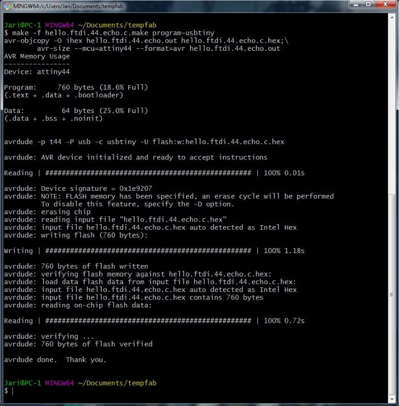
So now the test part. Removed my programmer and left the hello world board attached to usb port. Checking which COM port it was attached.
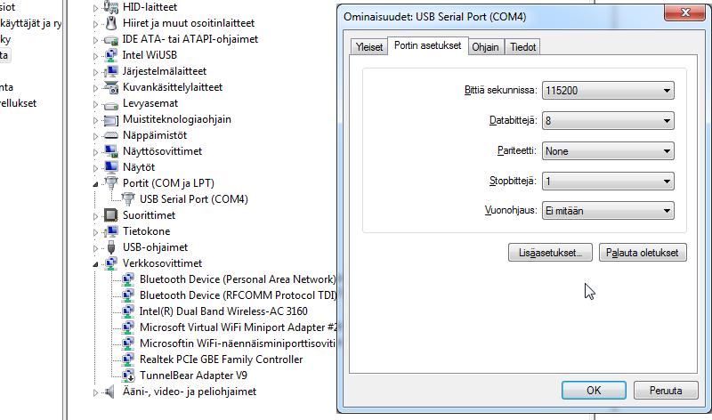
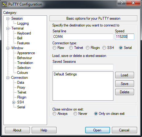
Using putty to connect to COM4 with 115200 speed.
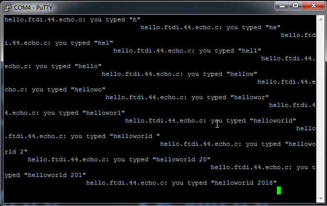
Typing will now echo. Success!
Group project
Group efforts can be found here(when its done).
Files

