Output Devices
Table of contents
Introduction
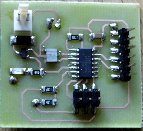
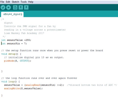
For this assignment I decided to control a fan using an ATtiny44 with a NDS355AN mosfet, as the driving electronics. The ATTiny44 firmware was written within the Arduino IDE and controlled the fan by pulse width modulating (PWM) the mosfet drive signal so vary the fan's supply voltage.
Electronic Design
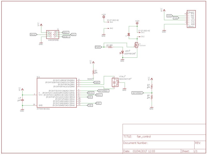
The board design was done in Eagle. From the schematic Q1 is the output mosfet and this is driven from Port B2 of the microprocessor. Port B2 is one of the IO ports on the ATtiny44 that can output a PWM signal. I also attached an LED and resistor to this port so that the LED would illuminate whenever Port B2 switched to a logic high.
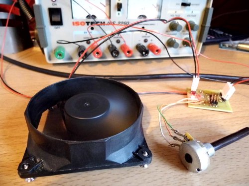
The fan was rescued from a power supply and was rated at 12V, 0.15A. The NDS355AN can handle 1.7A at up to 30V so is well able to drive this fan.
R4 and R5 are configured as a potential divider and their junction voltage is fed into Port PA7 which will be set up as an analogue to digital converter (ADC). This will convert the junction voltage to a digital number and allow the fan speed to be controlled accordingly. However when trying out the code I removed R4 and R5 and used a potentiometer to vary the voltage into Port PA7.
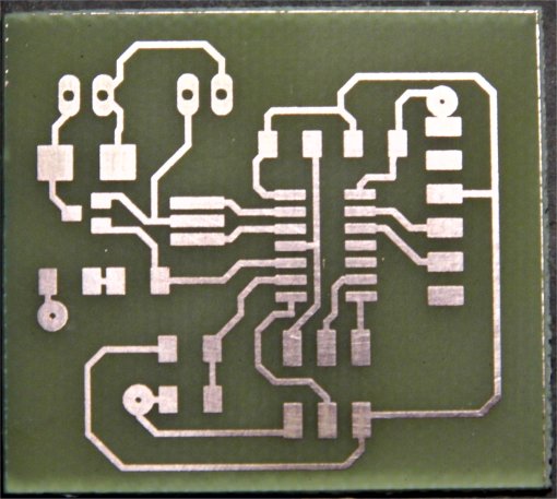
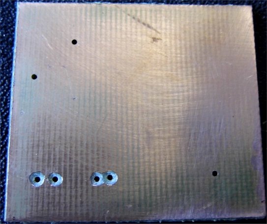
The board was designed as a two layer board with the bottom layer connected as the ground or 0V layer. This made it less complicated to route the board as it was easy to connect to the ground layer by placing a connecting pad on the top layer which would then connect via a wire link to the bottom layer. Note there was no routing on the bottom layer, it was a solid copper plane. When it came to manufacture the board, double sided pcb was used with the unrouted coper side functioning as a ground plane.
As I could not get access to the Modela MDX-20 machine in the Derry Fab Lab I made the printed circuit board by etching photo sensitive FR4. This involved printing the pcb trace layers onto semi-transparent paper( Laserstar), placing this over the photosensitive FR4 and then exposing this to UV light for approximately 3 minutes. The board was then developed using sodium hydroxide to remove the unwanted photoresist and then etch in a tank of ferric chloride to remove the unwanted copper and leave the pcb traces.
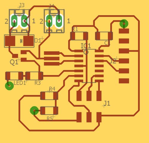
The assembled board along with the bare pcb is shown below.
Arduino firmware
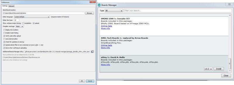
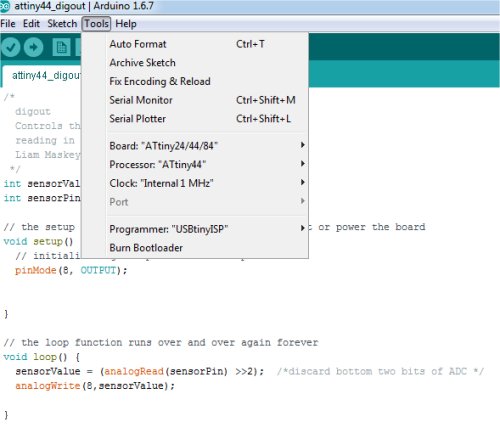
The firmware for the output devices assignment was developed in the Arduino IDE. First thing was to add the ATtiny44 processor to the Arduino development tools. This is acommplished within Arduino IDE by selecting File->Preferences and pasting the following link in the Additional Board Manager URLs text box.
https://raw.githubusercontent.com/damellis/attiny/ide-1.6.x-boards-manager/package_damellis_attiny_index.json
Click ok and then select Tools->Board->Board Manager and install the attiny boards.
Once the ATtiny boards have been added a new Arduino sketch was created and the ATtiny44 processor was selected which was configured to use the internal 1MHz clock and the USBtinyISP programmer. All these options are selectable from the Tools menu.
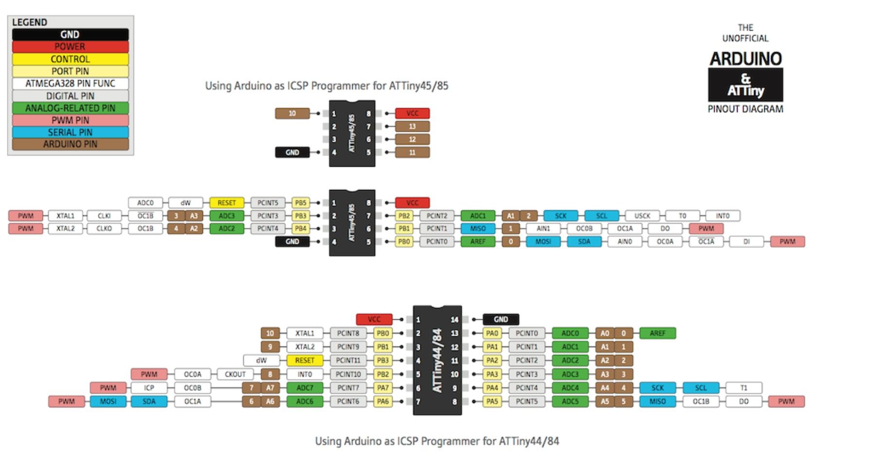
When developing the code it is not clear how Arduino assigns the port pins: for example what pin number does the Arduino IDE expect when Port PA7 is being setup as an input. The image below lists how the Attiny pins are mapped within the Arduino development environment. Click on the image to view full size
The Arduino sketch code is shown below. Essentially it reads in a voltage on PA7 and based on this value, varies the PWM duty cycle to PB2 which in turn drives Q1.
When programming the electronics using USBtinyISP select Sketch->Upload using Programmer.
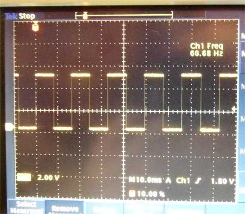
The working electronics is shown below along with a scope plot of the drive signal to Q1 indicating a 50% duty cycle. One thing I am not clear about is why the duty cycle frequency is so low at around 60Hz.