redraw the echo hello-world board
This assignment was my first aproach to electronics. Redrawing the hello-board was great understand the worflow of designing a board, using Eagle and also making me face the problems that came up.
After the Eagle introduction I proceeded to add the components from the fab library in the hello-board schematics window. I also named and connected the components by adding labels.
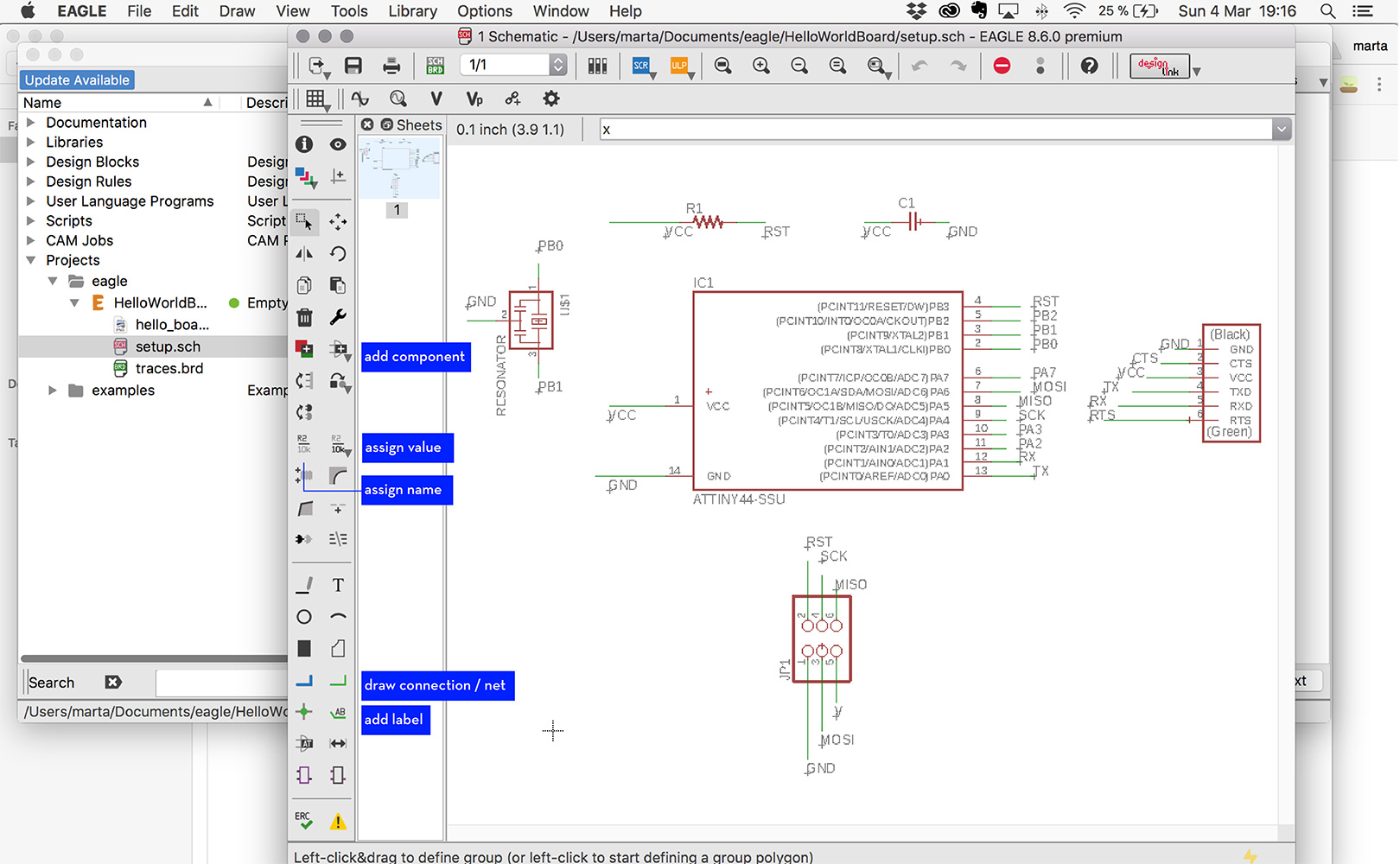
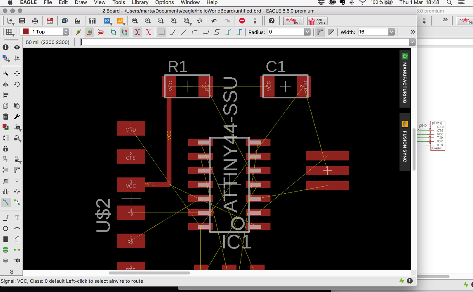
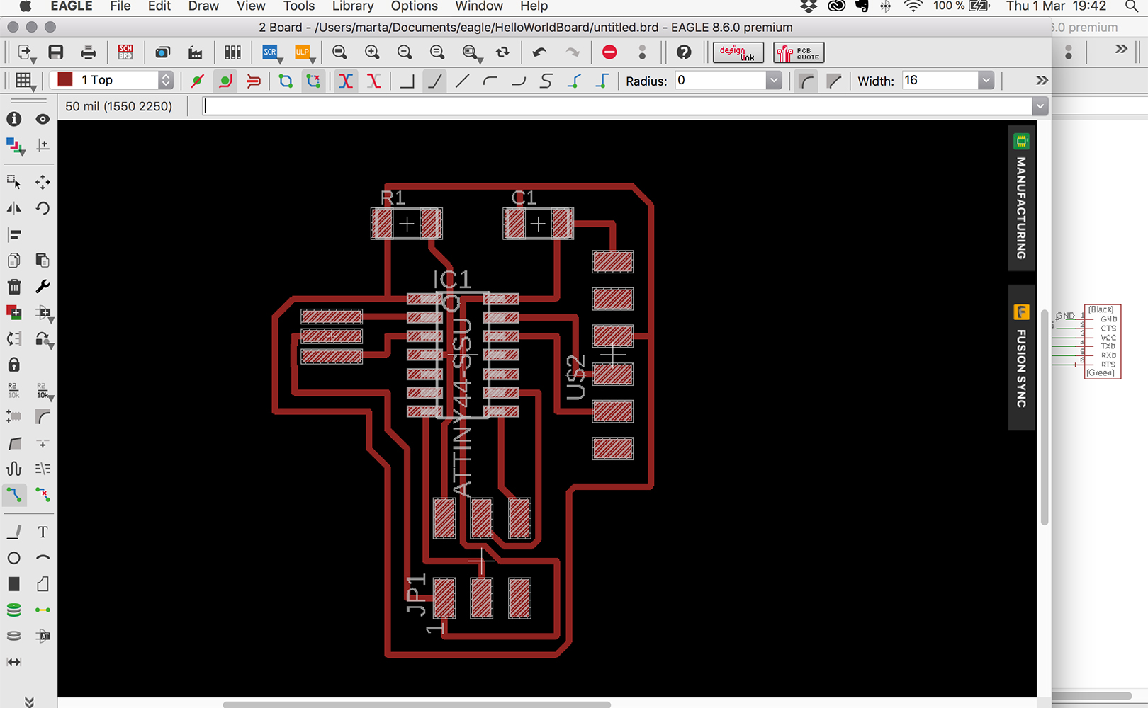
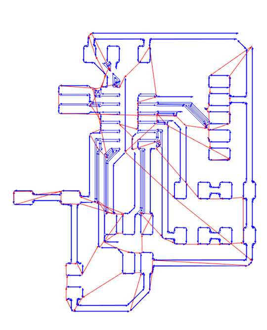
After all the components were setup in the schematics I moved on the the board window. Here it gets easier to understand how everything connects together and the final shape the board will have.
The tricky part comes when the yellow lines must be connected togther. It took me a while to find a way that everyhting joined properly without crossing. Some good advide is to move or rotate the elements around to find a way that the yellow lines look less tangled up.
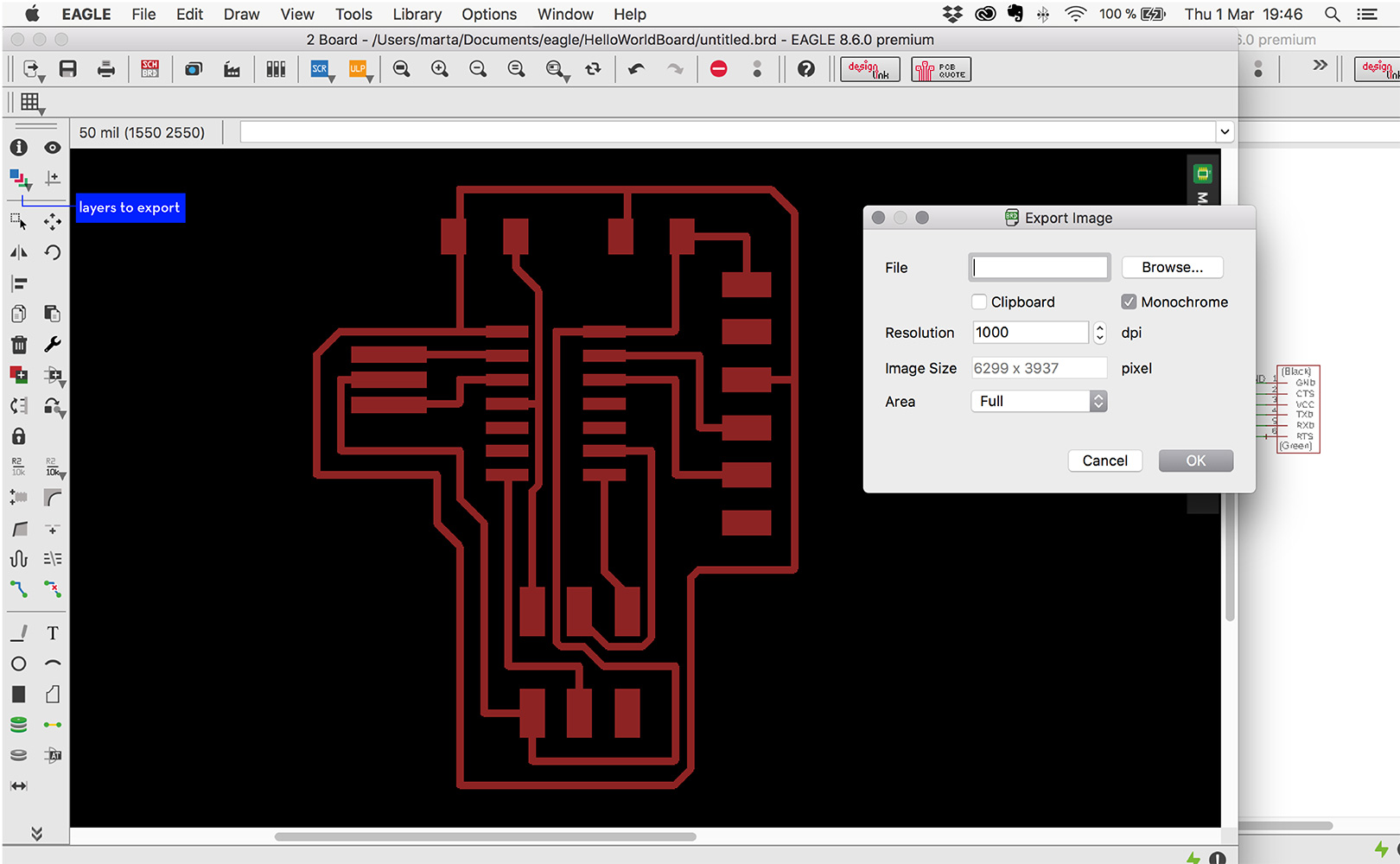
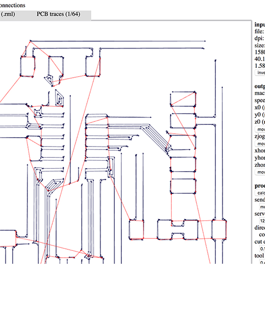
When exporting the board into an image, it is important first go to "layers" and select the ones we want to export. Normally it would be only the first, which will be the traces. Check the box for "monochrome" and make sure the resolution is at 1000dpi.
After this is done we open this file on Photoshop to cut it into a smaller piece and get rid of the black space and to alsogenerate the outline
Files:
Hello-board schemtics(.sch)
Hello-board board(.brd)
Hello-board traces(.png)
add at least a button and LED
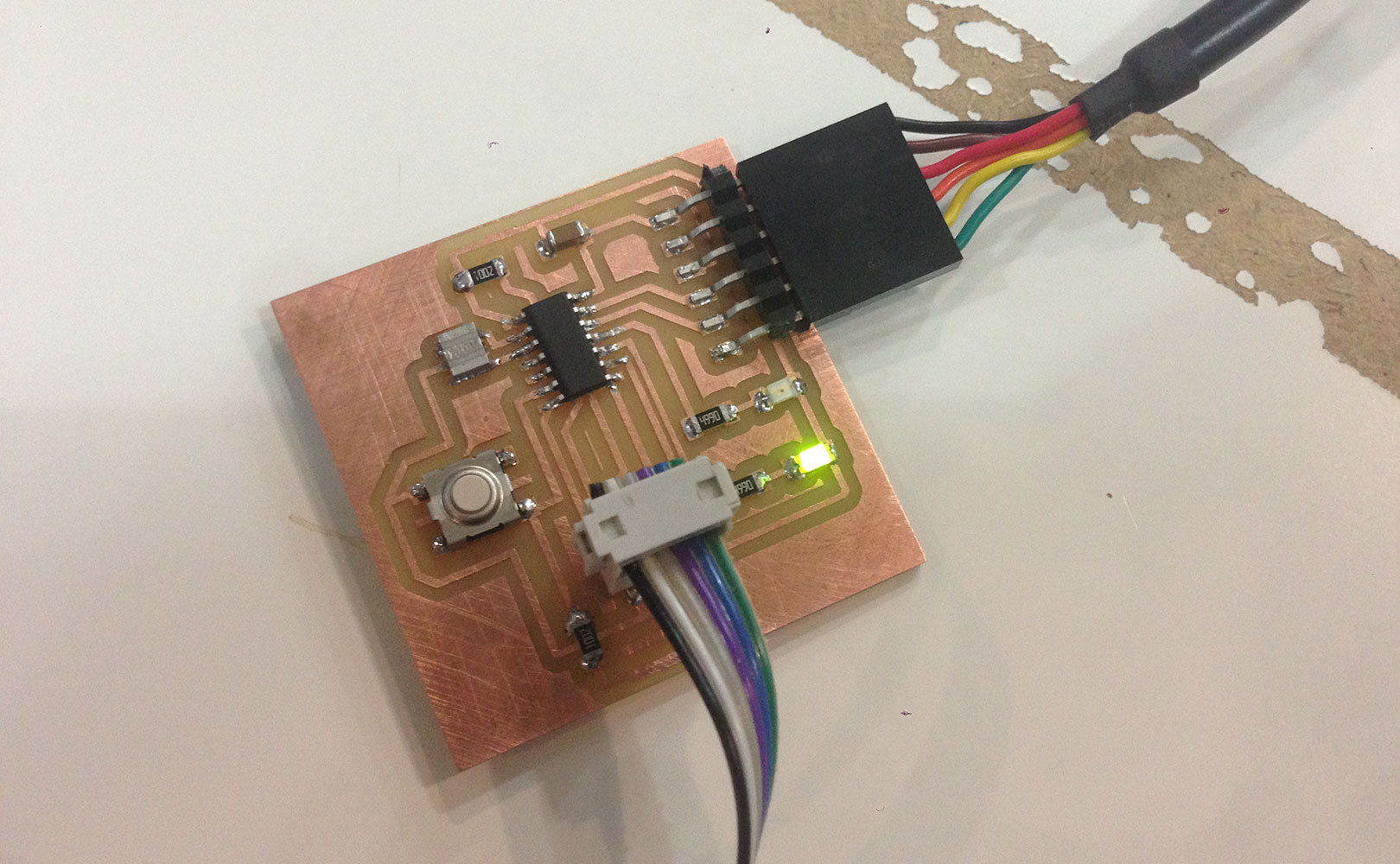
I decided to add two LEDs and a button.
I realized that when you add a LED or a button you need resistors to regulate the ammount of current they receive. For the LEDS I used 499ohms resistors and for the button 10k ones. I was surprised of how much easier whole the process became after I managed to stop trying to visually understand the schematics and just foccus on the connections between the components.
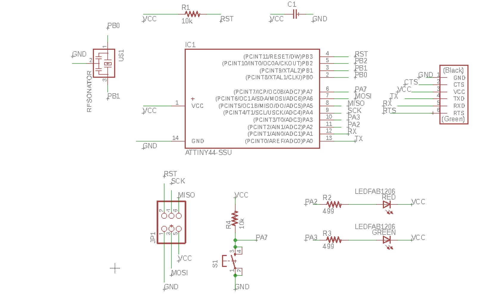
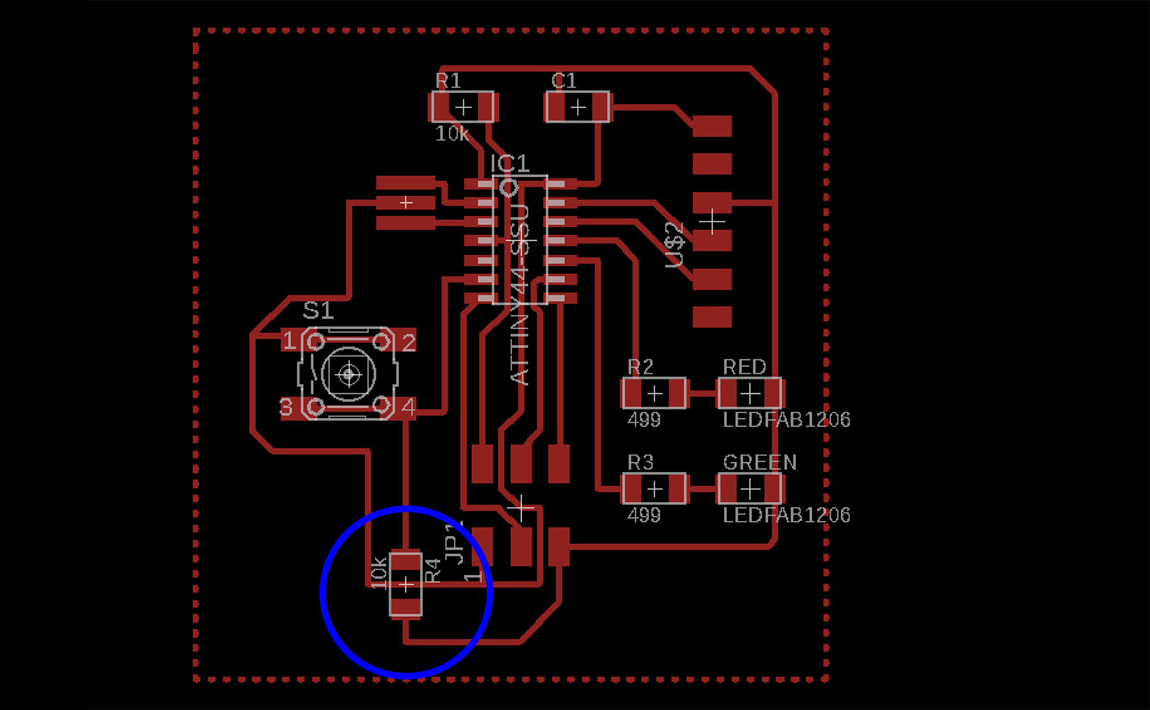
Once the extra elements were added I moved to the board window. I set all the parameters in the Clearance window to be 16mil and the line width to be 16mil. too.
I spend a really long time trying to fit all the components together. A good way to fix this was to first setup the components just like in the hello-board, and then trying to fit my new components in the empty spaces. Even though, I add rotate one of the resisors and cross over to a circuit line (image below) to make everything join.
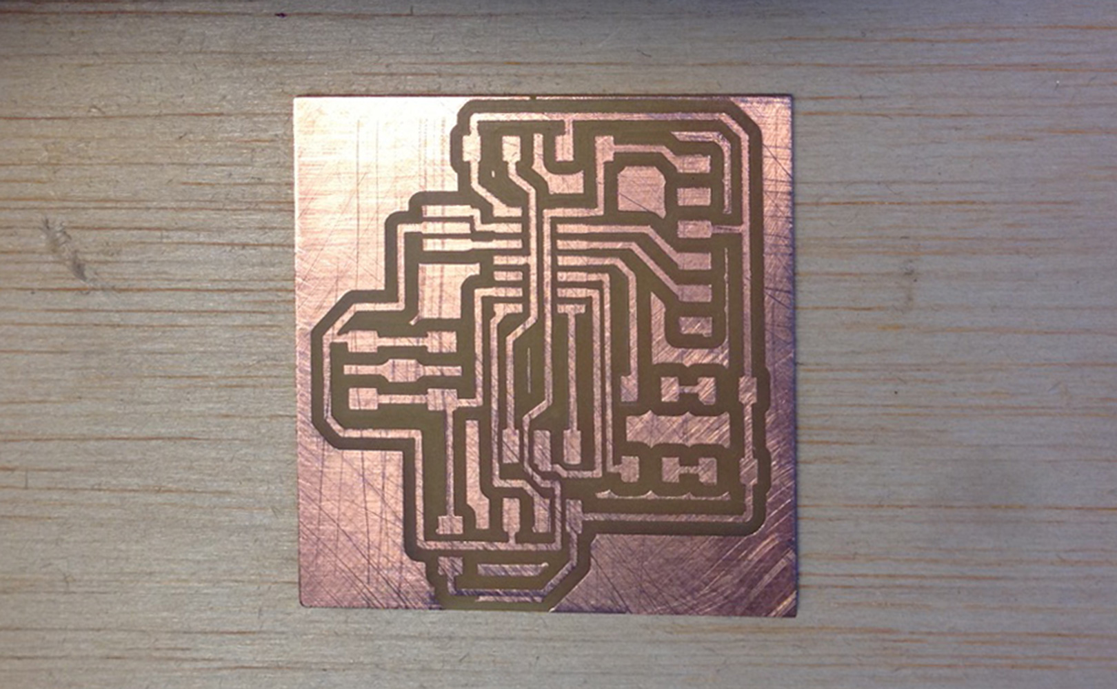
Milled and cleaned board below. Next time, I'd like to give a shape to the cutout, probably a circle, and also to make my board smaller.
- Remember to always setup the line width before starting to work, otherwise you'll have to change all the lines one by one.
- Always check board as you work by going to DRC icon > Clearance > Check.
- Type "run bom" command on Eagle and you get a list of all the components in your circuit, which is useful whem you have to get the components for solding bom (bill of materials)
problems this week
Issue 1
When the final board is exported as an image from Eagle, once you open it in Photoshop with a MAC it shows the board twice the size.
Solution: Reduce image 50% in size so that we can work with the real size board.
Issue 2
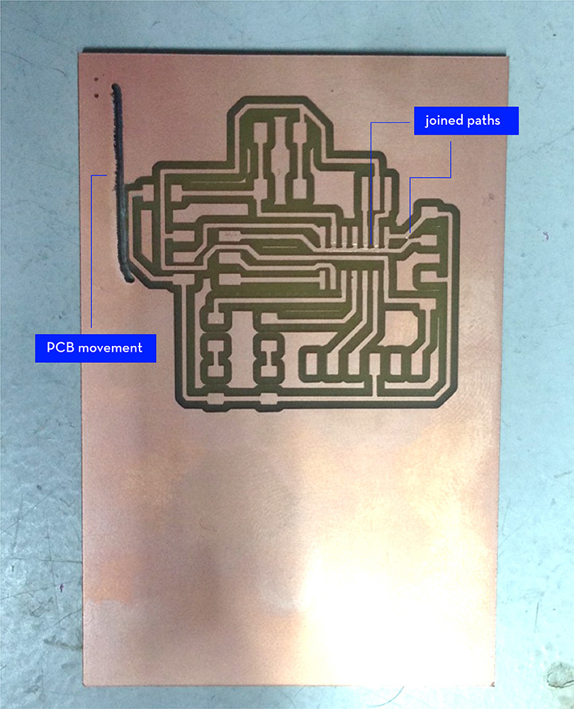
Opening exported png from Egle on MAC, processing it with Photoshop and later on using that same file to generate the .rml, causes problems at generating the milling traces and paths (images below). I tried to do it both from fabmodules and modes but still having the same issues.
Solution: Doing the same process but with a Windows computer instead of a Mac. It was necessary for me to generate the .png file using photoshop from a Windows computer.
Issue 3
After I calculated the milling paths on FabModules some circuits appeared joined together in places where they shouldn't. That would a caused a shortcircuit. It appeared that the lines where too close together and fabmodules was merging them for some reason. It is strange because I was not getting any errors when I checked on Eagle.
Solution: To go back to Eagle and give more space inbetween to the lines.
Issue 4
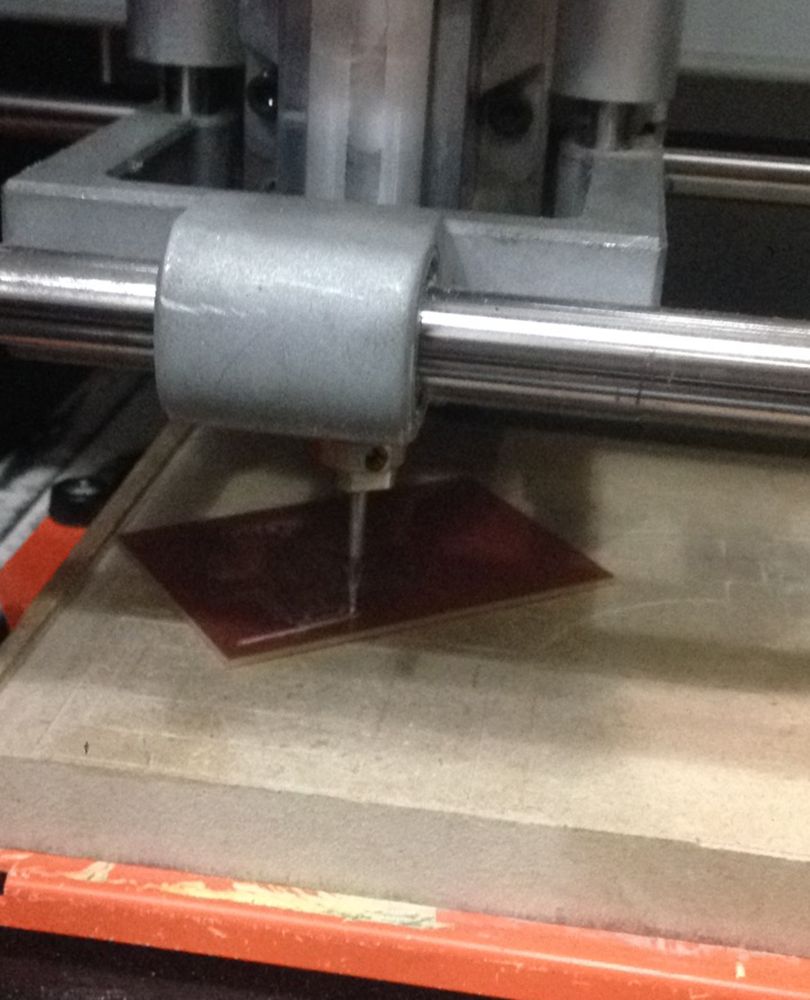
While the mill machine was cutting the outline my board got detached from the base and moved, causing a cut which ruined my board.
Solution: Make sure the board has enough double-sided masking tape on the back side and that it is firmly and securely stuck to the wooden base.
Files:
My Board schemtics(.sch)
My Board board(.brd)
My Board traces(.png)
My Board cutout(.png)
My Board traces ready for milling(.rml)
My Board cutout ready for milling(.rml)
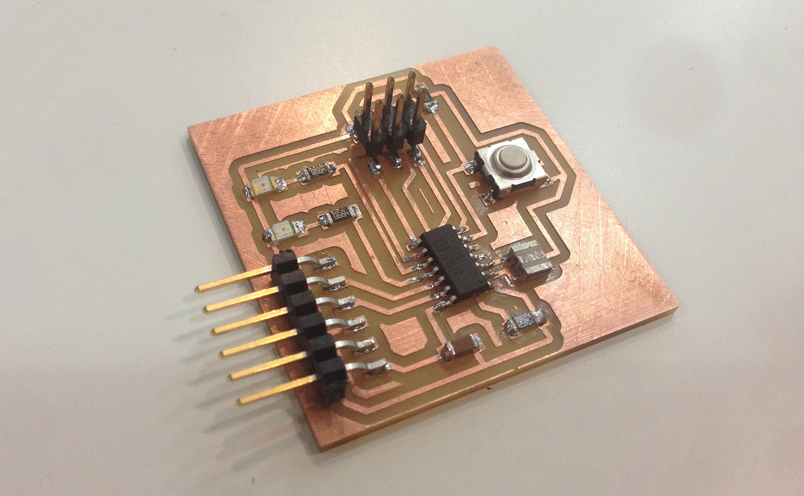
Programming my board
I decided to program my board with Arduino, it could also be programmed through the USBTiny Board we did a few weeks ago. There is this nice tutorial that explains how to program the ATtiny with Arduino.
I followed the steps, first adding the ATtiny chip to Arduino, then creating the make file: we declare all the items we are using from the Tools menu (Board= ATtiny24/44/84, Processor=ATtiny44, Clock=External 20 MHz, Port=usbserial, Programmer= AVRISP mkll). When all this parameters have been declared, Arduino creates its own “make.file” int he background.
We connect board to the computer and also the board to the programmer which will be connected to the computer.
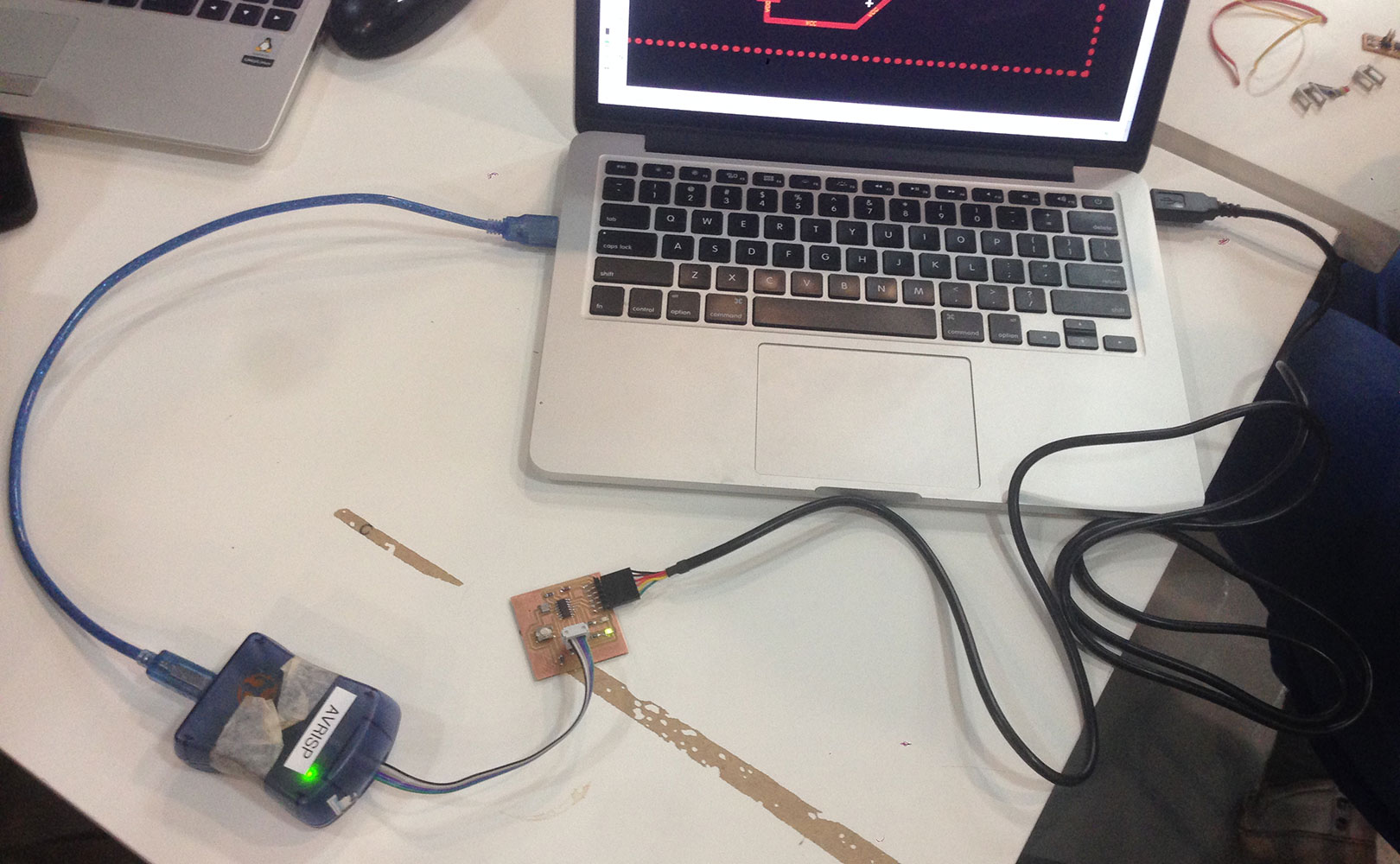
This is the moment to burn the code we just created inside my microprocessor in order to delete and clean my ATtiny from any possible previously burned inside. In order to execute this go to Tools > Burn Bootloader.