Gustav Kirchhoff and Alessandro Volta legislators

The behavior of electronic circuits and components, follow their own laws.
The possibilities that open when you know them are endless.
Sensors, transducers, actuators,... allow interacting with everything
and everybody.
The aim of this week is to start the study of these electronic laws. It
involves modifying a PCB with an actuator and a feedback (button and a
LED).
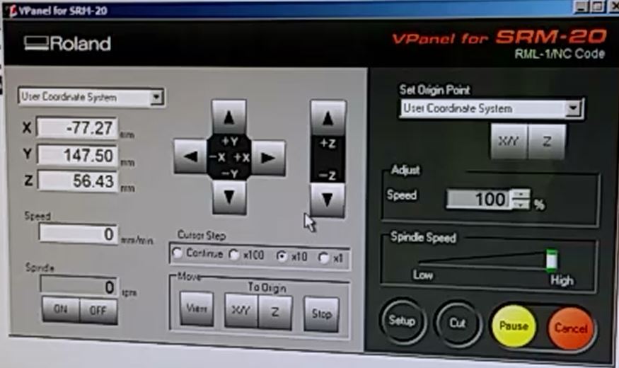
Load the Neil's board on Eagle software, add a LED and a Button, export traces, set the mill machine (Roland SRM-20), mill the PCB and solder components.
Content (linked):
AssignmentS:
TUTORIAL ELECTRONIC DESIGN

All documents are from 2015 Fab Academy web page, week 6 electronic design.
You can download them from here:
hello.ftdi.44.cad
board
components
traces
interior
programming
According to Eagle web page:
EAGLE PCB Design Software is the tool of choice for thousands of engineers
worldwide. With 3 modules and a common interface, EAGLE offers a variety
of product combinations and allows every user to choose the configuration
that meets their individual requirements.

On the top bar menú, click on Downloads/Download Eagle. It will open the
Downloads web page. There are Windows, Mac and Linux version. In my case
I have download Windows and Linux versions. There are self extracting archive
that guide you through the setup process. I have chosen freeware
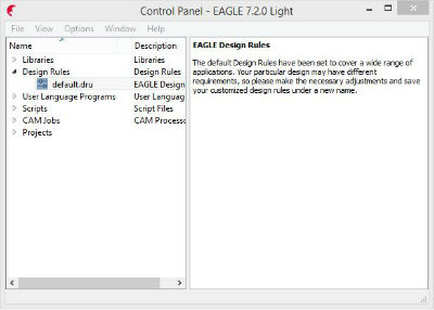
After installing, first it appears control panel. These are the main options:
Libraries: All the parts and components available. For our work, we have
a library with all Fab Lab components. Here it is the library:
Download Eagle Fab Library
Design Rules: All parameters relevant to the board and its manufacture.
User Language Programs: Funtionalities.
Scripts: Scripts to automating things.
CAM Jobs: How you export the board to fabrication.
Projects: Here we will put the schematic and the board design.
Select Projects, on the upper menu: File/New/Project and give it a name.
It will show a green dot wich it means "the project is open".
Now create the schematic: right click on the project name New/Schematic.
Now Schematic windows open. This is the area to design our board.
On the upper menu bar, click on "Generate/switch to board" to generate
a board and linked to the schematic.
I prefer to work with both windows opened at the same time but you don't
have to, you could switch between them.
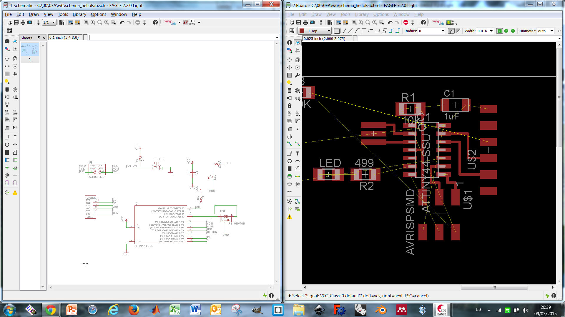
Working simultaneously with board and schemantic
On the left side there are the tools like components, traces, dimentions,
etc. It is also possible to use the command bar at the top of the screen.
In order to add a new component, type add in the command bar or click
on the "ADD" buttom on the left bar. It will appear all the components
and libraries.
Get into the Fab Library and add one by one all components. Look
for each component, choose the surface version, click ok.
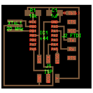
Connect all components as desired with wires.
Ground is another component is called GND. Add it as any component.
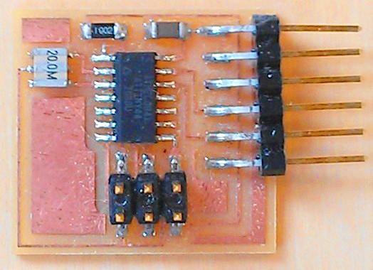
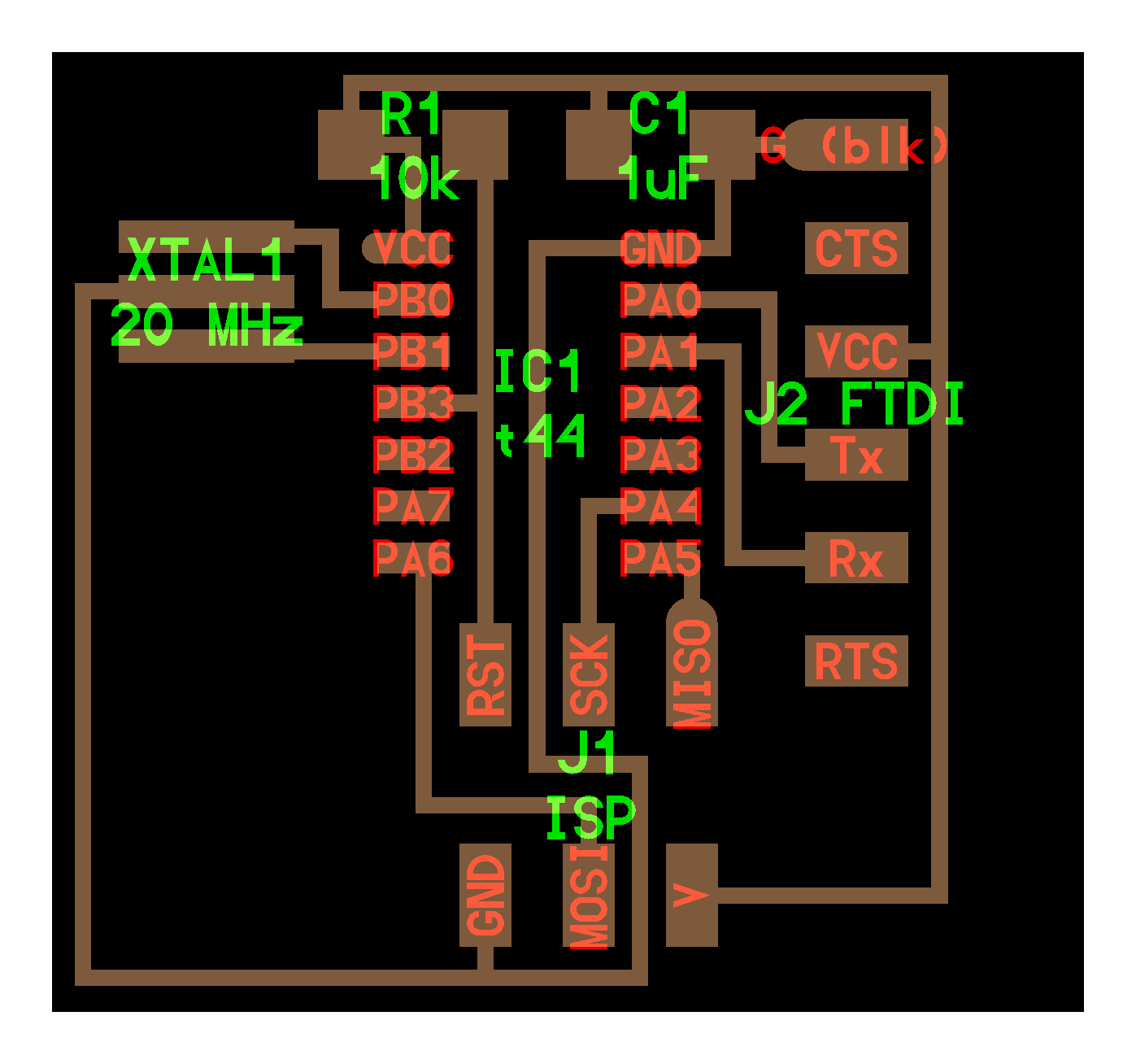
I have add a LED (with a current limiting resistor) on pin 6 and a button
on the pin 10 of the ATtiny44.
This is my final Schematic:
Download Adolfo's Schematic
On the Schematic upper menu bar, click on "Generate/switch to board" to
generate a board and linked to the schematic.
Now you have the connections but it is needed to create traces and
final boar size.
Put all components into the work area, click one by one component and
move it into the work area and try to move the components without crossing
traces (if it is possible).
Click on Layers button: There are top, buttom, pads, vias, dimension (it
need to be reduced by left mouse click on the dimension borders and resize
them).
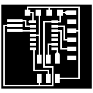
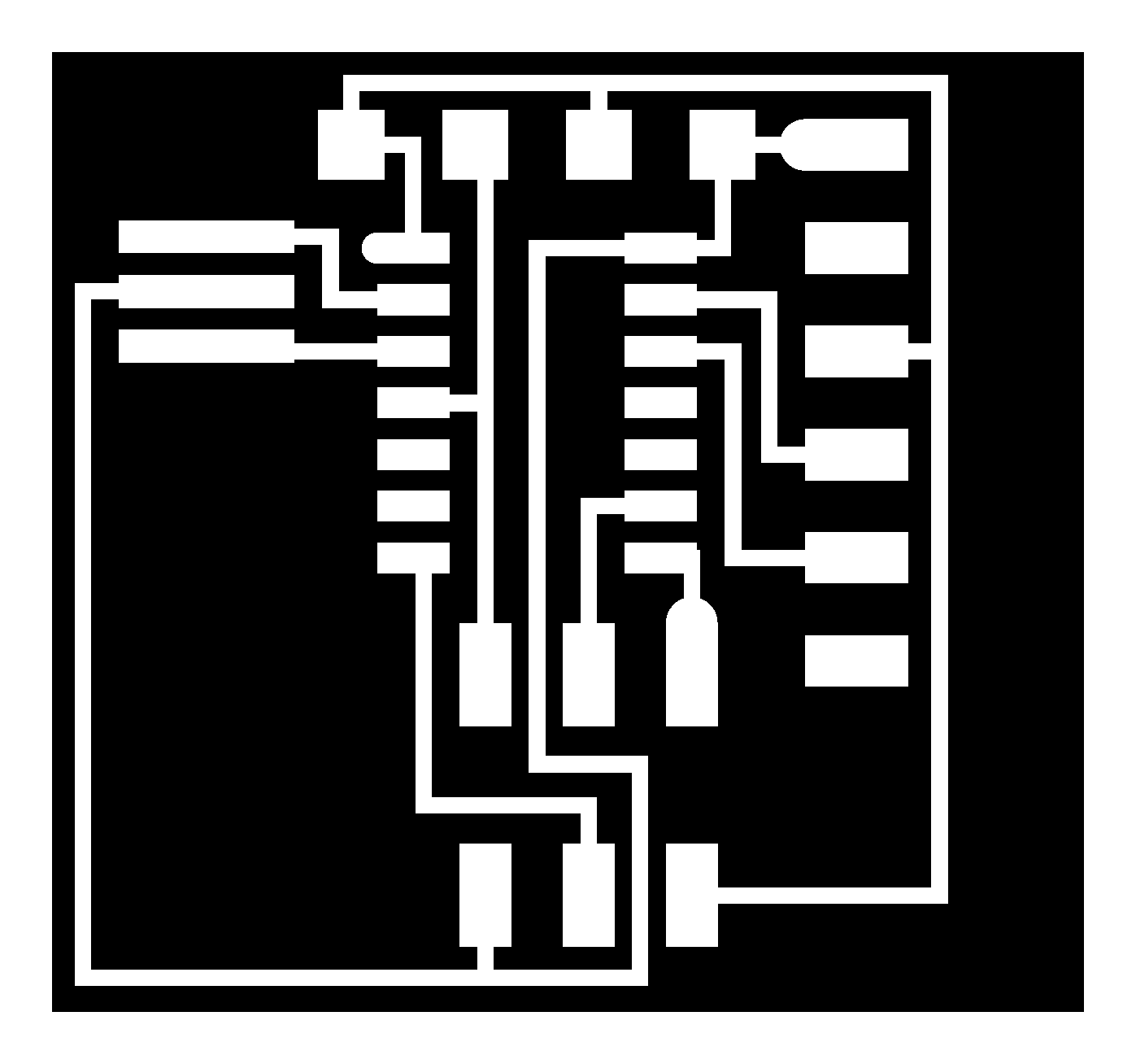
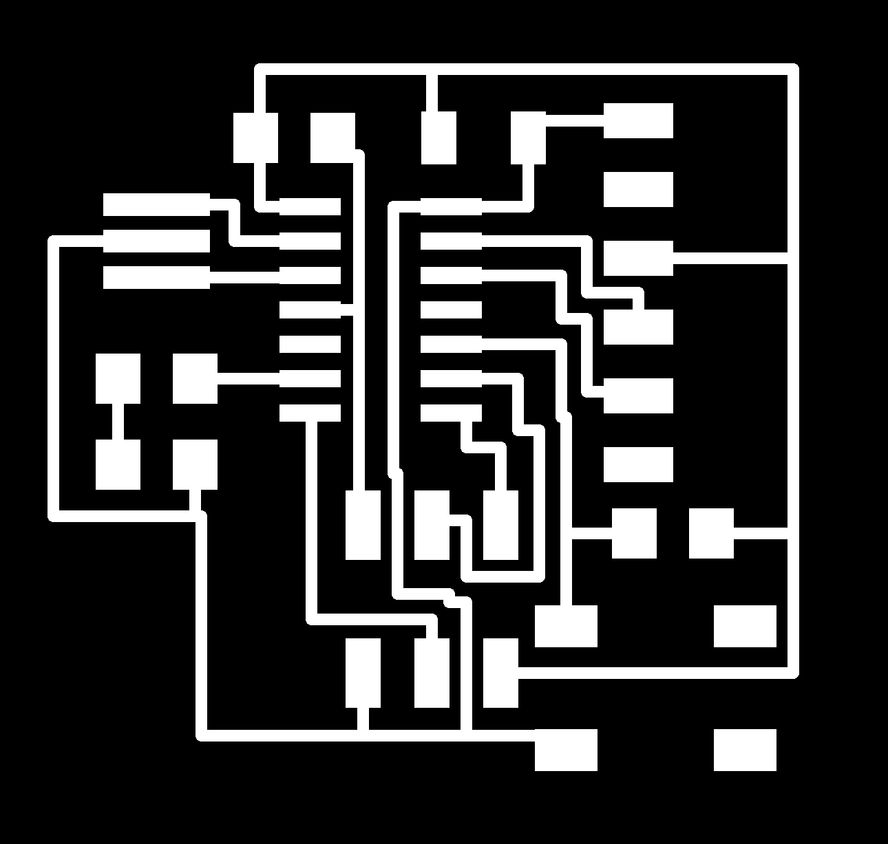
When every component is on place, then export the board like image file:
File/export/image and save it to your disc. I have used 600 dpi resolution.
This is my final Board:
Donwnload Adolfo's Board

I used GIMP.
According to Wikipedia: GIMP (/ɡɪmp/; an acronym for GNU Image Manipulation Program)
is a free and open-source raster graphics editor used for image retouching
and editing, free-form drawing, resizing, cropping, photo-montages, converting
between different image formats, and more specialized tasks.
You can download and install for free at www.gimp.org.
There are many ways to prepare the image to me milled, this is how I made.
I think is easy and quickly.
Open image
Select by same color tool all white area
Select fill tool
Select black color
Fill all white area with black color
Repeate with traces:
Select by sabe color tool all traces
Select fill tool
Select white color
Fill all red traces with white color
Prepare a border to cut the PCB milled.
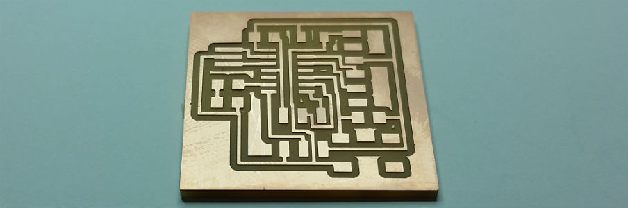
Download PCB traces png
Download PCB border png
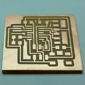
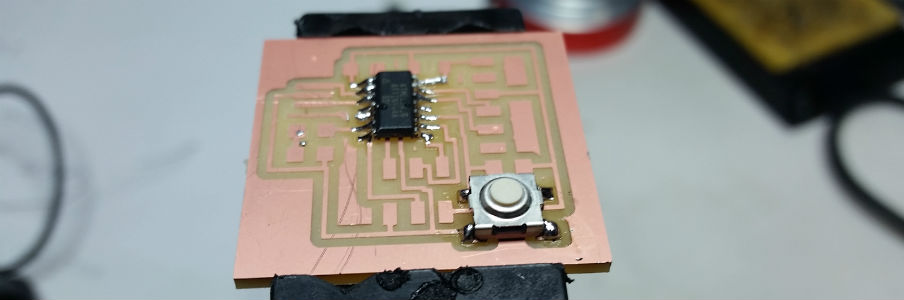
After milling, there are some scraps of paper and cooper. I whashed with soap and dry well.
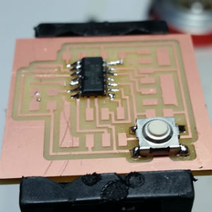
For me, the best option to solder is to put the soldering tool first, warm up the area where you want to put tin, add tin and wait for a while until the tin is distributed all over the area. After that, take out the soldering tool.
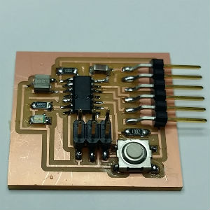
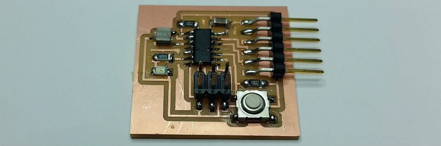
This is the PCB with all soldered components.