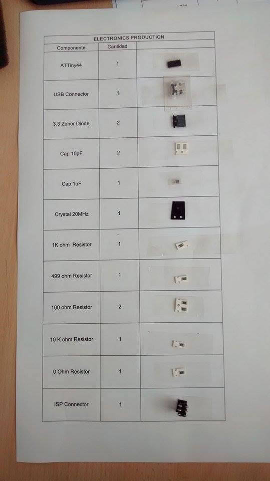
PORTABLE 3D PRINTER-SCANNER


STEP 4: ELECTRONICS PRODUCTION

Home

OBJECTIVE

- Build and program a PCB (Printed Circuit Board) or build a FabISP

PROCEDURE

DESIGN

1. I pasted a sticker on my board and put in the machine. Then I realized, that I had put the sticker in the wrong side, so  I took it out anc clean my board.
2. I downloaded the FabISP image in png format
3. I openened the Roland MDX-20 Modela's software
4. I selected "image png" in from Input format, Roland MDX-20 mill (.rml) in to output process, and clicked on "make_png_rml"

MAKEPNG

5. I clicked on "load"

LOAD

6. I browsed the downloaded image. I personalized the FabISP design that was available in the class webpage. I recommed to use few and big letters or it they are not going to be clear when printed.
7. For making the circuit traces I used the 1/64 inch mill, I clicked "3D plane" on type, wrote "1" on offset for not tracing the circuits more than one time, and wrote "0.9" on error for making a finer work.

DOWNLOADEDIMAGE

8. I clciked on make.path and the machine's movement path was shown

MAKEPATH

9. I closed the machine safety window and clicked on "View" botton and the header went to the left side of the machine
10. I adjusted the 1/64 tool with a screw driver
11. I changed the coordenates to a safe place where I could adjust the level of the tool (80x, 50y) and clicked on move to "xmin, ymin"

XY

12. I adjust the level with "Down" botton until the tool reached the board
13. I set new coordenates (20x, 20y) where I put my design
14. I clicked on "make.rml", "send it!" and "Begin milling"

BEGINMILLING

15. For making the external cut, I loaded the board png, changed the cut out board to 1/32 inch, type to "3D rough", top z to "0" (as the original position of the board is 0) and bot z to "-1.65" (as the board's width is 1.65). Then, I changed the tool with the scre driver.
16. I began milling.
Here I show the machine I used for milling the boards. modela

modela
WELD

1. I identified all the materials I needed for this assignment. I was given a paper with stickers to work with iny objects without loosing them.

MaterialQuantity
ATTiny 441
USB Connector1
3.3 Zener  Diode2
Cap 10pF2
Cap 1uF1
Crystal 20MHz1
1K ohm Resistor1
499 ohm Resistor1
100 ohm Resistor2
10 K ohm Resistor1
0 ohm Resistor1
ISP Connector1
Solder in station (not shown)
1
Tweezers (not shown)1
Solderwick (not shown)1
Flux (not shown)1
Brass sponge (not shown)1

MATERIALS


3. First, I began solding the AT Tiny 44, because it was the hardest piece to sold as it had polarity, which means that the anode and cathode could only point at one direction.

CATHODE


4. Then, I solded the resistors


SOLDING2

5. Finally, I solded the other pieces. The USB and Crystal were solded at the end.

SOLDING4

PROGRAM

1. I checked USB power by wrting "lusb" in the terminal

LUSB

2. I wrote "cd Desktop"

CDDESKTOP

3. I wrote "ls"

LS

4. I wrote "cd FabISP _mac.082_firmware/

FIRMWARE
5. I wrote "make clean"

MAKECLEAN

6. I wrote "make hex"

MAKEHEX

7. I wrote "sudo make fuse"

SUDOMAKEFUSE
8. I desolded the Zero Resistor
9. I connected the FabISP to my computer and the USBtiny was recognized! It should be highlighted that the code evidences that my FabISP was adequeately programmed.

USBTINY


CONCLUSIONS

1. I learned though error, that for an electronics and programming assignment, it is better to document while working, because too much information is learned and it might be forgotten.
2. One needs to be careful when changing the values when designing. I left "4" in offsets and my work lasted a lot.
3. Before solding, one must plan the order one is going to follow during solding.