Week 6: Electronics Design
3.4.2015 - 3.10.2015
Lecture Notes:
Homework:
- Redraw, mill, and stuff a copy of the Echo Hello World circuit
- Modify the original circuit to include one additional custom
circuit
- Optionally simulate it's operation
Resources:
- Fab
Academy Handbook
- http://academy.cba.mit.edu/classes/embedded_programming/index.html#echo
- http://academy.cba.mit.edu/classes/electronics_production/index.html
- http://fabmodules.org/
- http://kokompe.cba.mit.edu/downloads.html
- http://www.cadsoftusa.com/
Files:
- Modified Echo Hello World Circuit (FA Week 6 HW.sch, FA Week 6 HW.brd, FA Week 6 HW v01.sch)
Acknowledgments:
Many thanks to Andrew Harmon for his guidance on this project.
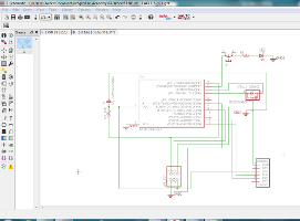
Circuit Design:
I used Eagle to layout the Echo Hello
World circuit (hello.ftdi.44) using the board image shown here
as a guide.
- Following Eagle installation I downloaded and installed the
fab.lbr. SparkFun has additional useful Eagle libraries
and tutorials.
- I familiarized myself with the schematic tools and added
hello.ftdi.44 SMD components from the fab.lbr.
Components were labeled when possible. The grid size was
left at 0.1 inch (2.54mm) to facilitate creating electrical
connections.
- Electrical connections were added using the Net tool,
checked using Tools > ERC, and modified when
necessary. Move, Rotate, and Mirror
tools were used to modify the components and keep
electrical connections as neat as possible.
- Once the essential hello.ftdi.44 components and connections were made, I added a simple button/resistor/LED circuit to pin PB2.
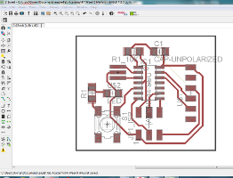
- With the schematic completed, I generated a board and
arranged the SMD footprints in positions similar to the
already optimized hello.ftdi.44 board. I gave
consideration for short traces and intersecting traces when
positioning the additional switch, resistor, and LED.
The Rat's Nest lines were somewhat confusing and gave the
initial impression some electrical connections in the
schematic were absent when they were not.
- I used the Auto Routing tool rather than manually
routing my traces. Prior to routing however I increased
the Clearances (Tools > DRC) within the wire-wire,
wire-pad, pad-pad, smd, and pad fields to 0.018 inch (0.46mm)
to accommodate the 0.015625 inch (0.4 mm) end mill. The
Auto Router tool was restricted to the top layer by
disabling bottom layer routing (N/A) in order to accommodate
single-sided milling.
- I tested and previewed the Auto Router tool with
low, medium, and high efforts and fine tuned component
positions when necessary before committing the traces.
- Using the Move tool, I resized the board perimeter
lines so they were closer to the outermost trace edges and
thicken them to 0.033 inches (0.84mm) to accommodate the
0.03125 inch (0.8mm) square end mill. Ultimately a
narrower line would have been more suitable (see Fabrication).
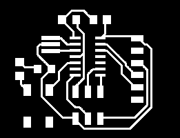
- I disabled all of the layers besides the Top layer
in preparation of exporting the circuit silhouette .
Additional text, component silhouettes, etc. would have
cluttered the trace silhouette and potentially led to
excessive and destructive milling.
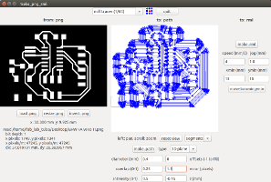
- Using File > Export > Image I exported the Top layer
as a monochrome, 1200dpi, full (not window) PNG file. Full
isolated the PNG to the circuit and kept the image size
reasonable.
- I used GIMP to invert the trace image and saved a new PNG
prior to milling it with the Fab Modules
- The board's perimeter was exported from Eagle in a similar manner after disabling the Top layer and enabling the Dimension layer. No color inversion was necessary for the board perimeter PNG.
Figures 1-3. (from left to right) Eagle
Schematic, Board, and Inverted Trace PNG
 |
 |
 |
Fabrication:
Milling the echo hello world board followed similar steps to
those used during Week 4:
Electronics Production.
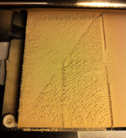
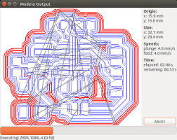
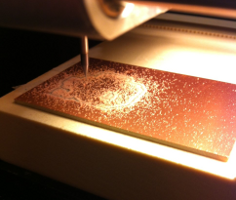
- Fab Modules were used to control the Roland Modela MDX-20
- A sacrificial substrate (polyurethane foam) was mounted to
the MDX-20's work plate and surfaced with the FR1 board
secured to the substrate afterwards using double-sided tape
- The trace and perimeter PNG files exported from Eagle were
separately loaded into the Fab Modules and 0.015625 inch
(0.4mm) and 0.03125 inch (0.8mm) square end mills used to cut
the dark areas of the images respectively. Default tool
settings were generally used however the number of offsets was
increased to remove most of the copper foil. The
thickness of the perimeter line resulted in multiple perimeter
cutting passes. Future perimeter lines will be narrowed.
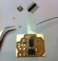
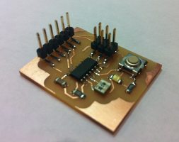
- Echo Hello World surface mount components were soldered to the deburred and fluxed board from the center outwards with attention given to the following: 1) orientation of polarized and multi-pin devices such as diodes and microcontrollers, 2) soldered joint quality, and 3) bridges. A green LED, 500 Ohm current-limiting resistor, and push button switch were added to the new circuit for pin PB2. The board was subsequently washed and scrubbed of residual flux residue using water and 90% isopropyl alcohol.
Figures 4-9. (from top left)
Surfaced Foam Substrate, Fab Module Path, Fab Module Milling
Window Output, Trace Milling, Soldering Components, and
Assembled Circuit
 |
 |
 |
 |
 |
 |