
Week 6
Electronics Design
Assignment
Check the design rules, and make it. Extra credit: simulate its operation.
I= current (Amp = A)
V=voltage
R=resistor (ohm) (omega)
C= capacitor(farhat = F)
L=inductor (Henry=H)
P= power (watt)
J= jumper
6. March
March 6th
I had downloaded Eagle in the morning and Bas was leading us through the process and I followed these instructions:
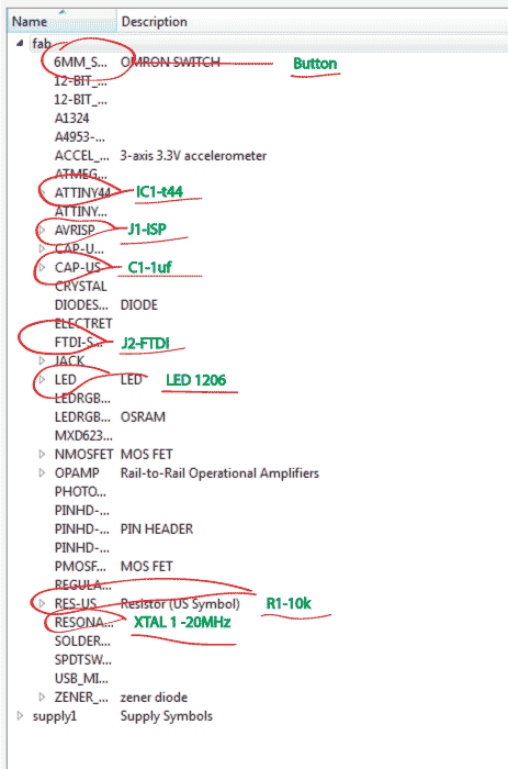
I created a special folder in documents for eagle. I opened it and then I created a new schematic board and saved it in the eagle folder. Then I went into libraries and I deselected them all but then chose supply1 library by changing the gray dot into a green dot. From the FabAcademy website I then found the fablib library - I downloaded it and I saved it in my eagle folder. Now I was ready to begin. I had a window open with an image of the board that I wanted to make - hello world board plus of course Eagle and my schematic board. I started adding all the pieces that are on the hello board into my schematic board. We used the red circled tools the most. I added the ground and the vcc just somewhere on the board and then I copied it and placed it at the right places. I connected everything together that is connected together on the hello board image with wire tool. In order to take away a placed wire I first chose the trash can and then the wire that I wanted to get a rid of. Here I had to be careful to place a junction where it was needed since on a schematic board the wires can go over each other.
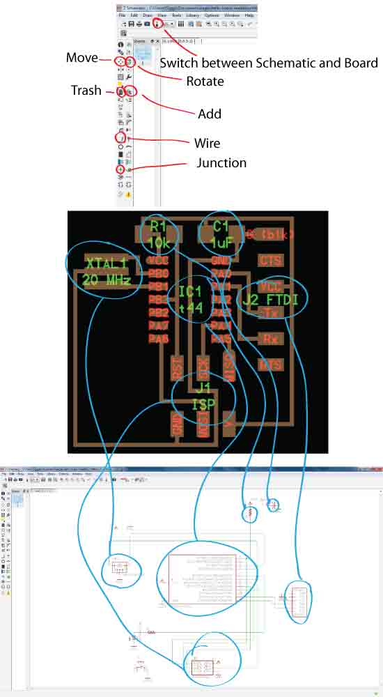
I added the button and the led once everything was in place (turned the right way) and connected I put in the button and the led. and a resistor with the led. The led was connected to number 6 and the button number 10.
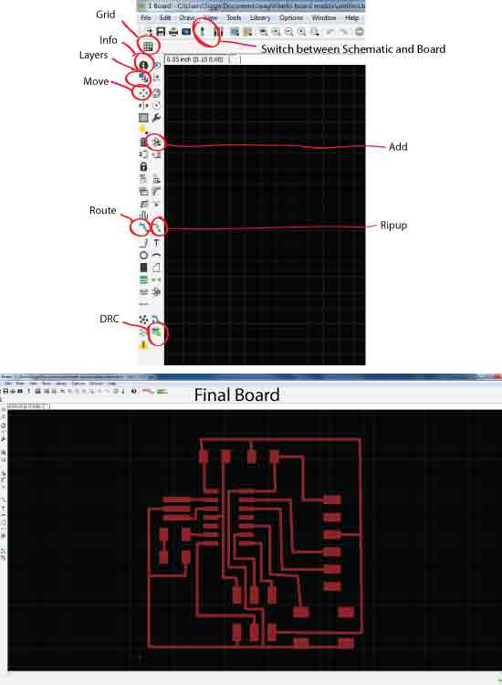
Then I switched over to the board window. Important to keep both windows open the whole time.
(Schematic file lost)
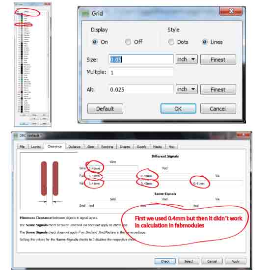
Now I used route in order to connect the yellow lines that showed me which pieces where supposed to connect. I was not paying attention when Bas said that the routes couldn´t cross so I was very quick but then I had to do everything over again with no cross overs. The grid helped a lot but it was also very helpful to go into info and use the number to move lines just a little bit. Once I was finished connecting everything I pressed DRC and opened clearance. There we put at first 0.4mm but then we had to change it to 0.41mm since we all had an error in fabmodules. Then I press check and the software gives me some errors that I slowly fix. The trick is to check every single time I make some changes untill I have no errors.
I make the image smaller by clicking and draging the white lines so they are just a little bit bigger then the traces.
I exported the board-traces by selecting the top layer only and exporting as png and 1200 DPI and I chose monochrome. Then I ussed the rect tool and made a blu rectangle on line on the grid larger then the white lines and we had layer number 20 dimension and the layer on the bottom of the list and then we saved the image as png and with the same settings as before. Then I opened it in Gimp and poured white in the middle of the image and saved it as my outlines. Then I opened it in fab modules to see if everything was looking so it could be milled and it all checked out.
March 9th
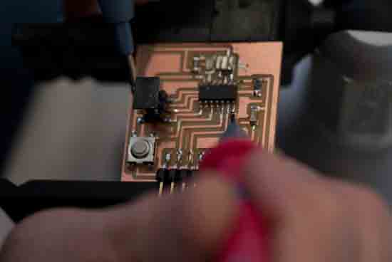
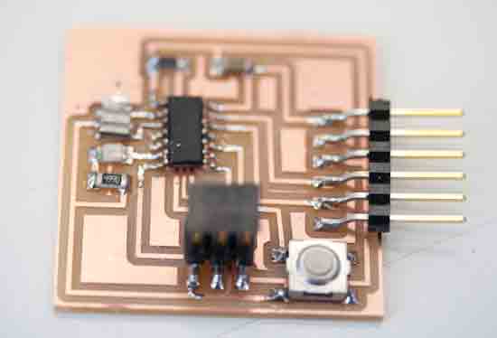
I put my folder on a chip and connected it to the computer since that computer has a hard time connecting to the fab serer. I put my file on the desktop and opened it from there in fab modules. I changed the cut depth to 0.2mm since we knew from before that by leaving it on 0.1mm it wastn´t milling all the way. Everything went really well and my board was ready not before long. I looked at my notes from week 4 beforehand so I felt quite comfortable.

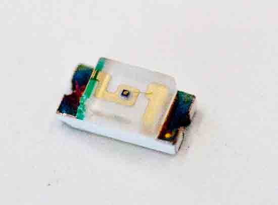
I found the pieces I needed while I waited so I was able to start soldering everything on the board. It went pretty smooth although I found it a bit hard to solder the crystal since it didn´t have those little legs to help out but I managed. I chose the red led and found out it needed a 499 resistor. We use the version of Ohm´s Law that puts R on the left side.
R=V/I R=3.2 V/0.01 A = 320 which means I need 499 resistor since it´s ok if the resistor is too big but it can not be too small.
Then I have to figure out which side is plus the side that should be closer to the microcontroller. I use this machine which I also use to check my connections when I finished solering.
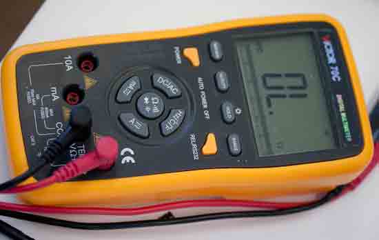
The led and the 499 resistor are the last pieces that solder on. Then I do the beep check. I check the connection between all the ground to ground and all the vcc to vcc.
I got a beep everytime so my board is ready.
Lecture from Neil
components
wire ribbon cable - pull off wires that we need. awg match the gage of the wire to the current…..
button connected internally
resistor: I=V/R grated by package, resistance, power
capacitor: C = Q/V, I = C dV/dt limiting current flow - it´s the derivative. Energy storage.
unpolarized negative and positive
polarized almost like a battery store huge amount of charge- used for local power source - it matters how it´s placed
crystal, resonator when you put voltage on it - it flexes. resonator is a 3 terminal device- and crystal is a 2 terminal device
inductor: V = L dI/dt derivative of the current - used to filter power
diode: current from anode to cathode only from anode to anode
PN
Schottky use to have flow in one direction
Zener used to clamp voltage keep it below a certain thing
LED have to use a resistor to limit the current
transistor
bipolar always drawing current: collector, emitter, base current gain
mosfet: source, drain, gate resistance - we use this one. lower power
battery, regulator on the high sight 30 volts - on the low 6 volts. if you put the battery on backwards you kill the regulator.
op-amp: differential gain, negative feedback
microcontroller built in amplifier and therefore we don´t need op-amp
sensors
actuators
circuits
Kirchoff's laws: sum current at node, voltage around loop = 0 add up to 0 sum of voltage
power: P = I^2 R = I V 10amps x 1om =100volts
EDA
hierarchical, parametric drawing
packages, footprints, component libraries
design rules
schematic entry, component placement, routing, simulation, fabrication
drafting tape
drawing
Eagle fab.lbr most of us will use - export an image - resolution 1200 - lots of libraries and support
KiCad gEDA open source design tools
OrCAD Altium commercial software - handle more complexity - from free to expensive
Cadence Synopsys Mentor Tanner Magic really expensive
SPICE LTspice ngspice gSpiceUI design tools for simulation
Gnucap Qucs Oregano
123D Circuits Virtual Breadboard Fritzing Multisim BLUE friendlier more visual.
Verilog VHDL programming language in order to manage complexity
fab modules pcb.cad
assignment
redraw the echo hello-world board, try different tools
add (at least) a button and LED (with current-limiting resistor)
check the design rules, and make it
extra credit: simulate its operation need a part library, check the design books - make sure that there is room for the machine. Design and program a board in an hour.