EagleCAD
I have previously used Altium to create circuits, but this software is not free and all the libraries for the components for the Hello World board are already there in EagleCAD, so Eagle it is!
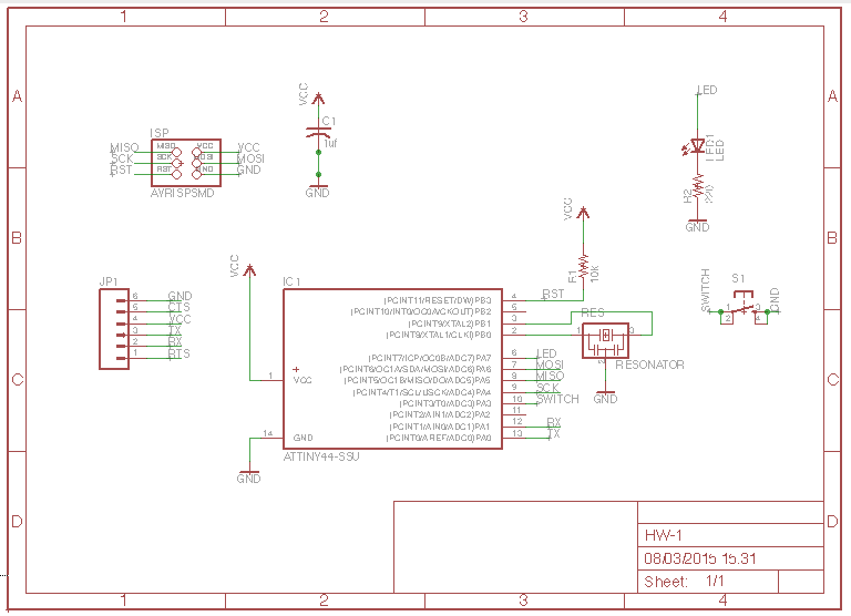
This week started off straight forward, follow the tutorial on editing the original Hello World board in schematic format and then transport that into board format. It seems simple but EagleCAD has nuances that can delay a new user in getting a good result. Firstly the schematic and board editor work together so closing one will affect the other because it does not transfer the changes. It also took me some time to work out how to do remote nets instead of wiring up manually. The issue was that I forgot to create a Net name, and then go about renaming it. I also managed to neaten it up by adding a frame (it seems silly to have to pick a frame, surely it should automatically frame your work?).
Copper Laser Etching and Engraving
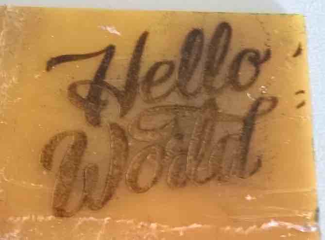
I found time to try some laser etching spray I acquired from a company awhile ago. I saw uses for it with labelling boards in specific areas (e.g. R1, R2, C1 etc).
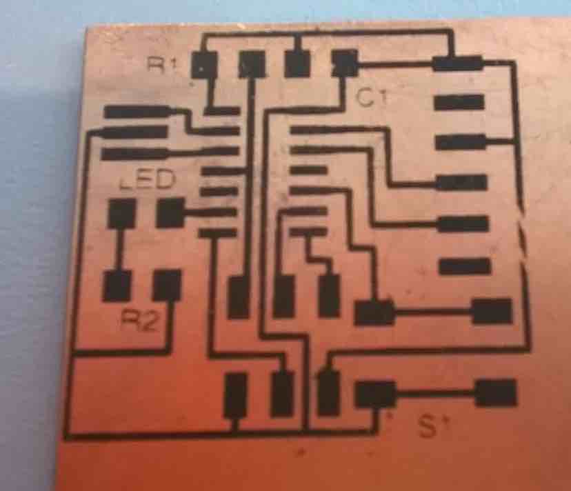
The spray is very simple but you need to play with the settings on the laser cutter to get a good imprint on the board without it rubbing off too easily. The first picture is my first attempt which just followed the original png file but with some extra labels for components. This worked well but it rubbed off slightly too easily. The settings on the Epilog Laser for etching were 50% Power / 50% Speed.
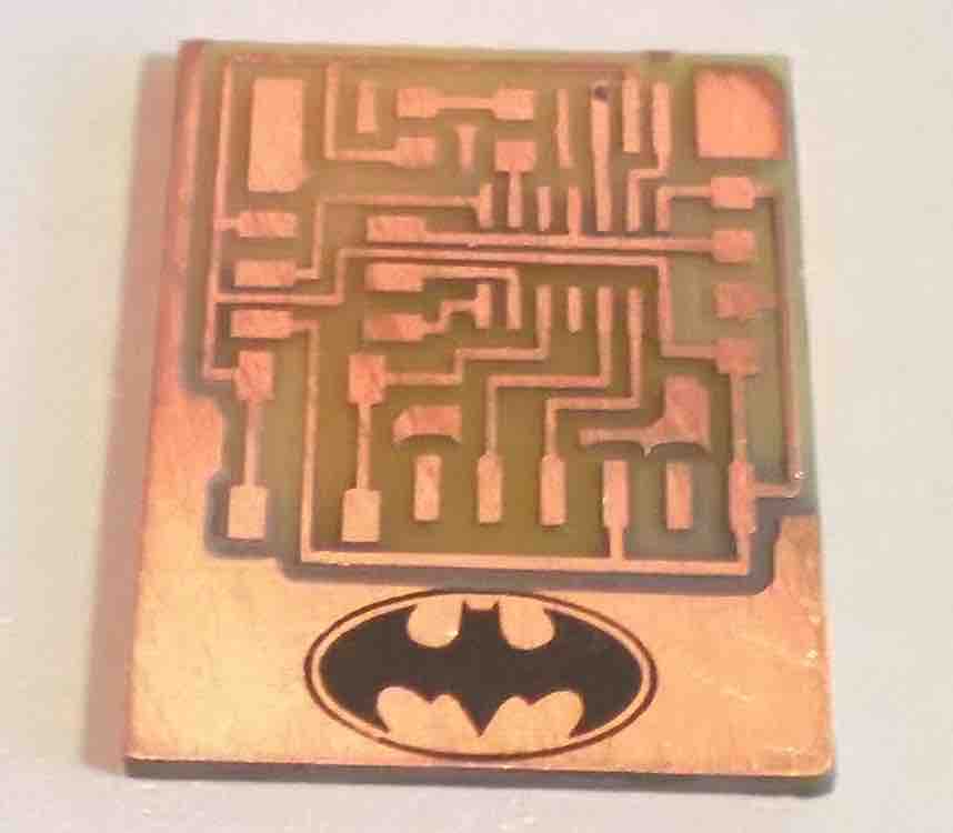
My next attempt was on my actual board, but I didn't want to try to label the components because I felt it wouldn't be that effective with the milling removing some of the available copper left for etching. So I tried adding an image on the right hand size that could be used to label the board, obviosuly it had to be the batman logo. This time I hade 60% Power / 50% Speed, this produced a more robust image which didn't rub off as easily. Maybe even more power next time for more perfection
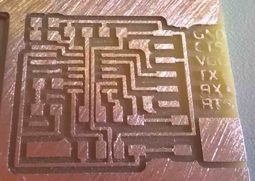
Using Eagle, I also created some text using the Eagle software. I wanted to label the incoming pins to show the polarity rather than just trying to work it out each time. This worked out ok but the text was too small for the toolbit to effectively give it a good finish.
My final attempt of changing the appearance of the board was to try and etch into the back of the board which I thought might get rid of the stickiness (it didn't). All of my attempts at etching or milling into the board were to make the boards more acceptable as opposed a fully designed board from a board house. I believe my findings show that it is possible to give the boards a nice silkscreen, but the results can be hit and miss.
Eagle - Electrical Rule Checks
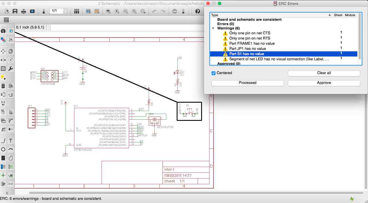
The first board I made had one major issue which I did not diagnose until I had made the board. This made me heed the advice of the electrical rule check (ERC), which I had observed before but did not notice one major issue which was the VCC and GND traces were directly connected (for which I have no idea how that happened). After this incident and wasted man hours trying to fault find the board, I went into the the ERC and checked the rules. There were certain issues where pins have no value or do not conect to anything (valid reasons), if I am happy with these, I can approve them and move on. I did try and go back and purposely make a mistake but the software did not recognise there to be an issue, I put this down to Eagle not being intelligent enough to recongise that VCC and GND should never meet directly. I am still trying to work out how to add this rule.
Eagle - Design Rules
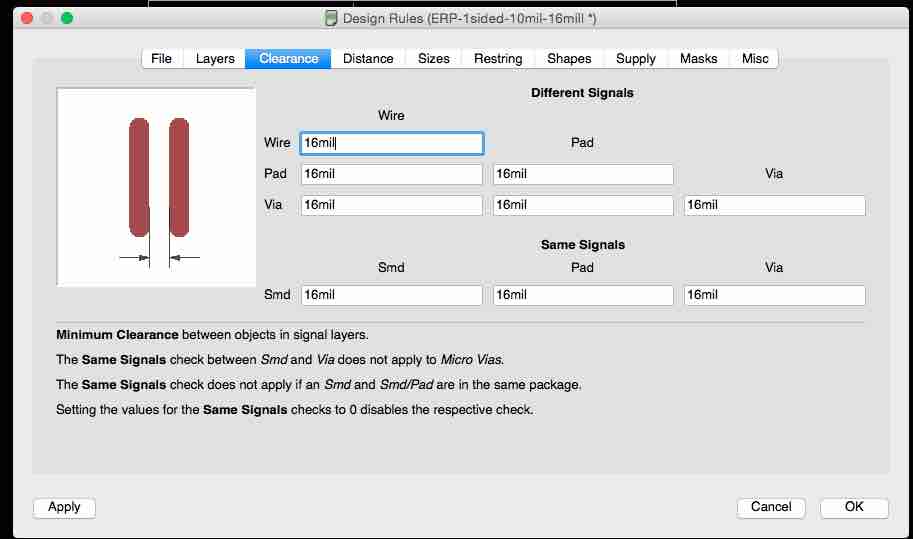
This is where I can set the minimum distance between the traces and the pads. The drill bit we use for milling is around 15mil, so 16 mil is used to keep a distance between them. I can also set the trace thickness in the design rules, if I have more power going to a certain component I can increase the thickness of the trace.
A guide on using EagleCAD
This is a rough guide on how to use Eagle to achieve a finished circuit board. Please note that the milling process is excluded from this guide as it is covered in more detail in a previous week.
- Install the Fabacademy libraries and footprints into Eagle using the lib folder.
- Open the Hello World project and begin to add the extra components needed. In this case this was the LED (1206), resistor (1206) and a push button. The push button does not need a pull up or pull down resistor as the attiny has an internal pull-up resistor inside, which helps with making space on the board.
- The easy way to add the components is to type in "add" which brings up the menu. From there I can enter the name of what I want on the board but with a * on eitherside of the name, this makes sure that the search looks for anything containing the name of what I entered.
- It is then easy to all the connections together using the line tool, but this gets messy so I give all the conections a NET and a corresponding name. This means that I can connect elements together that may not actually be attached on the schematic.
- Once I have joined up the nodes on the schematic, I can check the EDR for the board and check no immediate issues are found.
- I then go to the board view using the icon at the top. From here I can begin laying out the extra components onto the hello world board. This can be fiddly if you are new to creating traces in a board editor as it is easy to get stuck between the traces. With these examples it was fairly straightforward to get them all located easily.
- After this I did a design rules check which shows errors all over the board, I am not sure why but I have not set any of the rules for the board design. It is something I intend to investigate further in future projects.
- Once happy with the board, I select only the top layer which shows my traces that need cutting out, and I export them as a .png at a resolution of 500 pixels. This gives a clear image for the Modela to work with later. I also set the image to monochrome and save it
- Once I have a .png of the top layer of the board, I now need to create a border which the Modela will cut out. In order to do this I open the .png in Gimp and change the canvas size to be 40pixels taller and wider (20 pixels on each size), and then centre the image. I now have an image with a border of 20px all the way around
- I now flatten the image to take out all the layers in the images. I change the border colour to black and export this as the traces .png, I then press CTRL + Z and make the border white again. I then invert the image and delete the internal traces until they are all white. Now I have a black border around the border which will cut out. I then take both of these files to the Modela for milling
Initial Testing
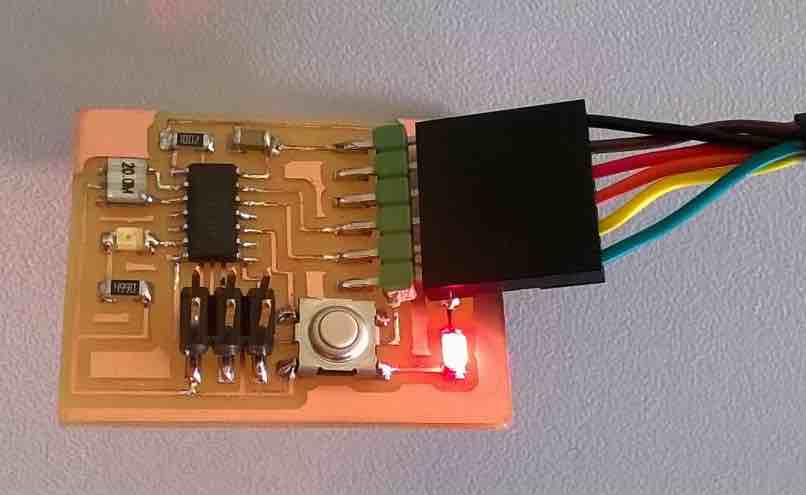
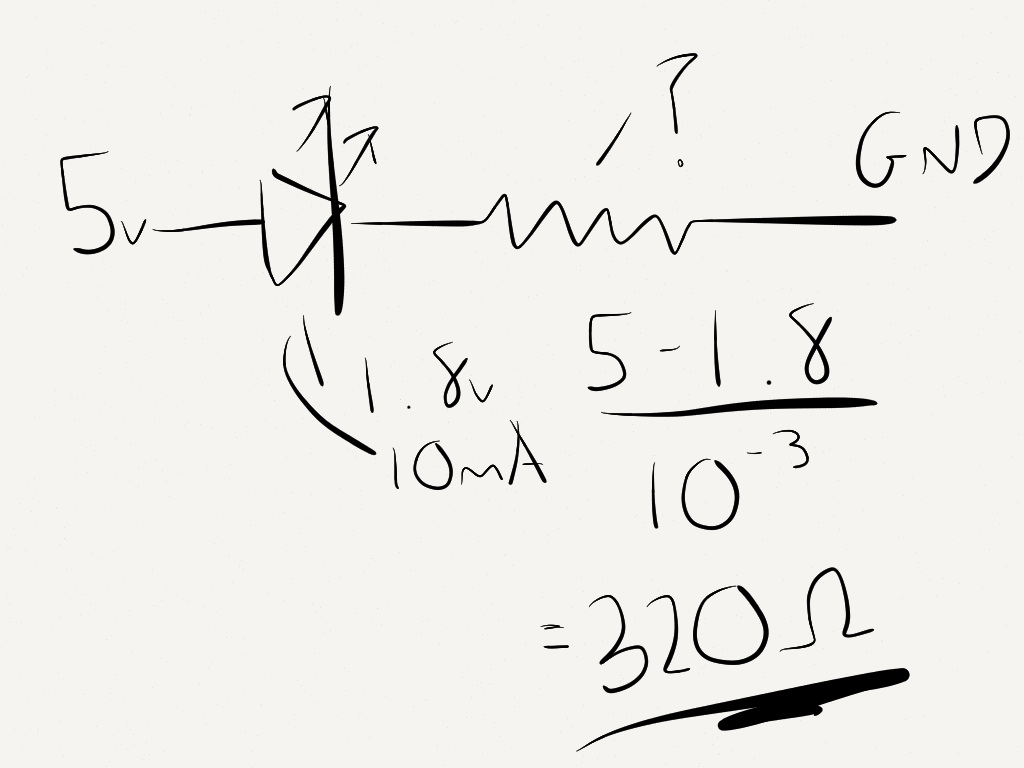
Without wanting to wait a week to see if my board worked, I set out to check it simply with my tutor Michael. I am not paying attention this week to the process of configuring the board (that's next week) but I did manage to get my board to do a basic arduino blink programme. There were teething issues such as me forgetting to solder one of the FTDI pins which meant the board had no power, but it eventually started working. There was a brief moment where the board was not working properly (the green LED was really dim), I checked the LED was OK by passing 5v across it and the resistor, it was fine. I then thought the board was broken so I decided to make a new one...
The 3rd board I made was really the board I wanted to make in the first place because I added a red LED and resistor in parallel to the VCC trace, which showed when the board was powered up. I soldered it all and powered it up (yay red light!) and it programmed fine through my ISP header and Macbook. I then decided to check my 2nd board again, and repgrogrammed it and it was fine afterall. I'm blaming that on one of the computers at FabLab!. So now I have 2 working fab boards, time to programme them to do something interesting.
An exploration into circuit simulation
Please watch this space whilst I try out simulation packages
