week#6. Electronics design.
What is the goal?
For this week we have to do simple "hello, world!" in pcb: a little board that would have at least one single LED and a button on it. Just to get a feel of what electronic design is.
Of course that would be a little to tough to make that from scratch, so we had an example (you may see that on the right)
For this week we have to do simple "hello, world!" in pcb: a little board that would have at least one single LED and a button on it. Just to get a feel of what electronic design is.
|

|
We also needed to try as much CADs as possible. But the road of a thousand miles begins with one step and for me this step will be the Eagle-cad.
The mighty eagle.
My first shot was to try to work with this CAD without tutorial (because I thought that if I have an experience of working vith some vector-2d-cad systems (autocad, inkscape, corel draw), finding out how does this one work won't be difficult) and that was a mistake. Althoug I really understood some principles intuitively, some other I didn't and that was a little frustrating (To be more correct, I could not find a way to translate my schematic into the board view). Luckily, following
this tutorual from dabacademy archive helped me to get through all this troubles and get further to face some other.
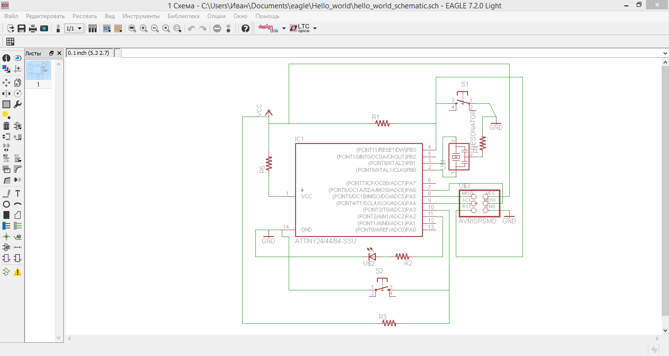
sch & brd
In eagle you can switch between two mods: schematics and the board. What is the algorythm of designing your own pcb?


|
First, you use the schematic mode to put all the components you need and draw the circuit diagram. I am not really sure that I have nice one, but I like it (the first picture on the left)
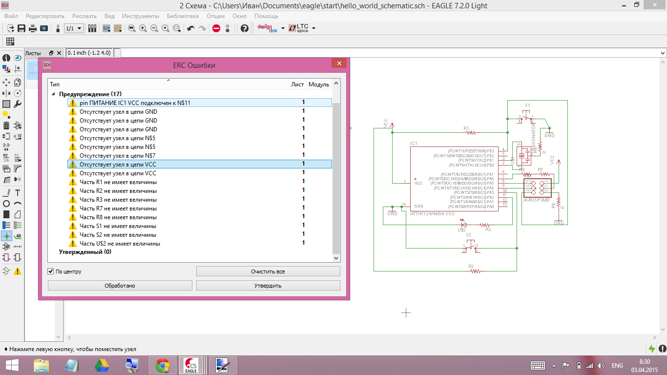
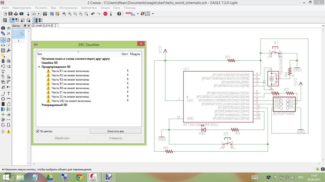
But when you think you're done, that doesn't matter you really are. Right, time to debug!.
I've added some joints and all errors left are about writing the components values. That's not good to leave that as is, but I'll fix it a little later.
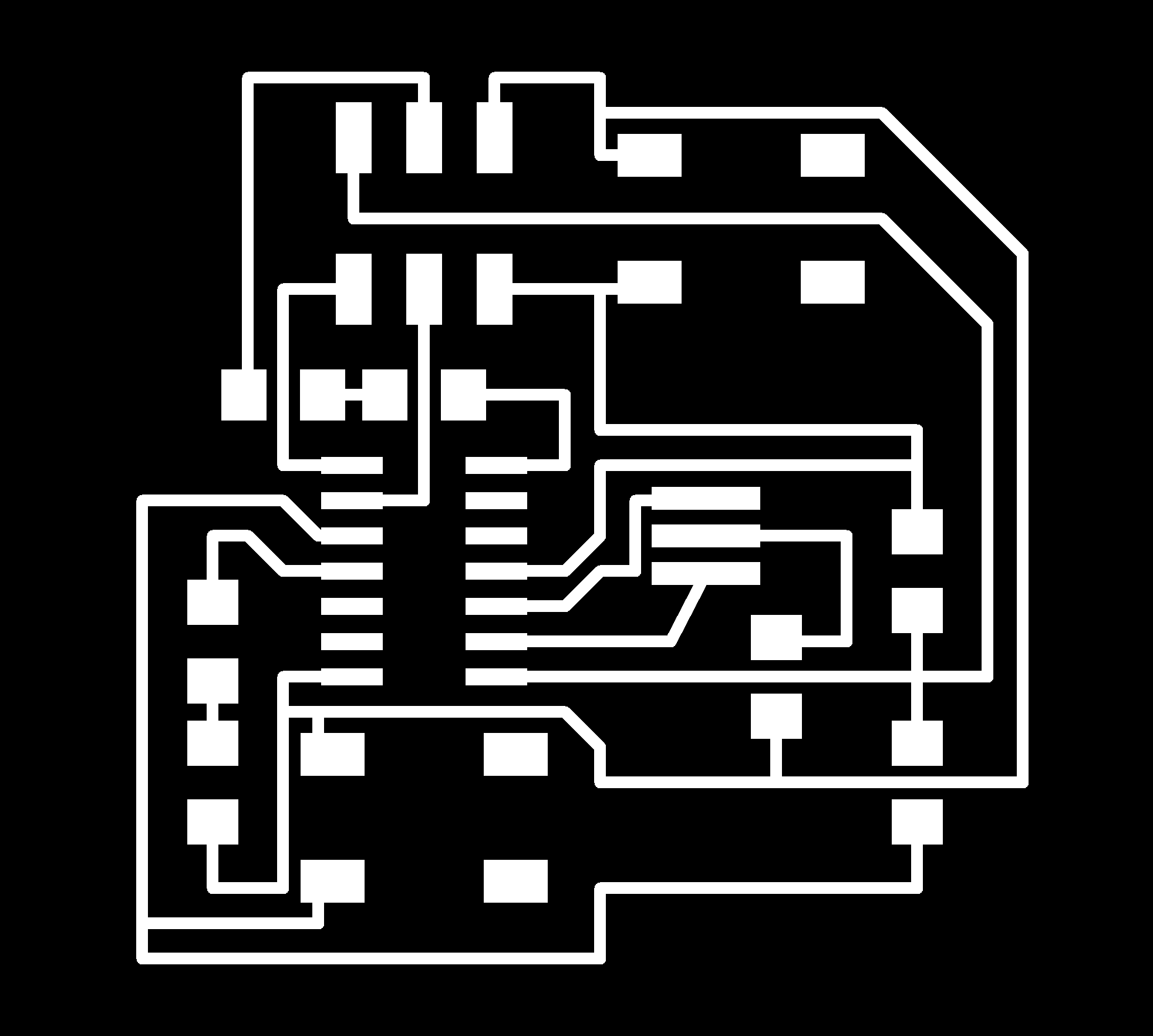
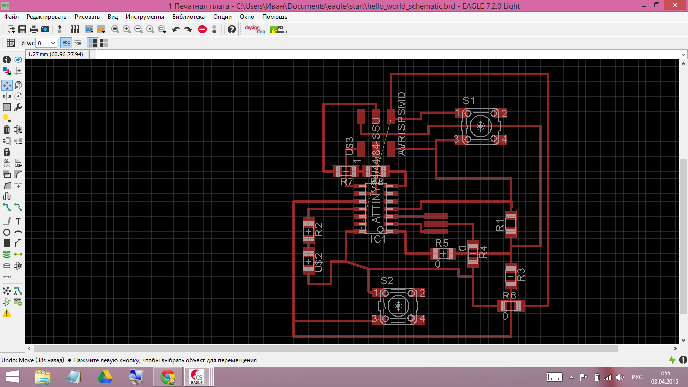
Then you need to switch to the board-mode and try to trace your pcb. At first that may look as a perfect mess (see the picture at the left). But be not afraid to make the next step: routing.
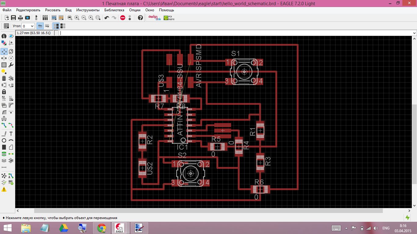
In little steps you can walk far if you have enough time! Almost done!
Don't try to make everything perfect at once. I belive you will be able to do that later, when yor skills get sharp. My routing was really sparced at first.
But then it became almost nice and compact.
Then you need to switch to the board-mode and try to trace your pcb. At first that may look as a perfect mess (see the second picture at the left). But be mot afraid to make the next step: routing.
|
So, what do we have?
That's what I have as a result so far. I would like to change pins to one-row headers, but for now this revision will be ok.
Here are my hello_world schematic and hello_world board files!
After milling ang soldering it looks loke this:

But actually while programming I had to debug it and remove almost all the copper filling:

Programming
watch my next week assignment to see the programming of this hello-board!
Back to my assignments-list
Back to my main page