Week 6 - 3D Electronics Design
Brief
The brief for this weeks assignment was to learn how to use Eagle and modify an existing circuit. The modification was to add an LED with a current limiting resistor and a button.
Eagle
Having had very little experience with Eagle I chose to follow this tutorial to create my circuit.
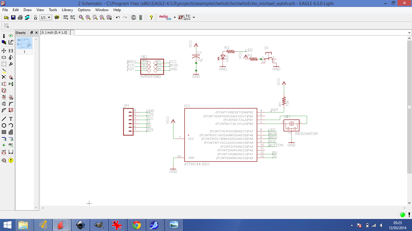
After installing the libraries I got to grips with how to navigate and type commands such as "add" to insert components. The board schematic window is where each component must be added and pin connections can be sent to gnd and vcc. Each connection/label made in the schematic window feeds the board layout window, which is then used to export the traces and cutout layers. One of the most useful features of the schematic window was the net command. Net labels on each pin of a chip create a link between the labelled pin and the corresponding area of the schematic, I found this the best way to route the pins of the tiny 44.
In the schematic I had to choose 2 resistor values, one for the current limiting resistor to be connected in line with the LED and the second as a pull up resistor to be connecte to the button. When choosing the current limiting resistor I used the values in the datasheet of the LED (1.8v, 40mA), V=IR and this handy website to calculate that I required a minimum of 82 ohm resistor. Looking at the stock of components in the lab it seemed appropriate to choose the next resistor up that wasn't too close to the theoretically safe value, so I chose 499 ohm resistor. After doing some research I found the pull up resistor value in a 5v cirsuit is typically between 5-10k and so as the tutorial stated to use 10k, I did.
Here is my schematic
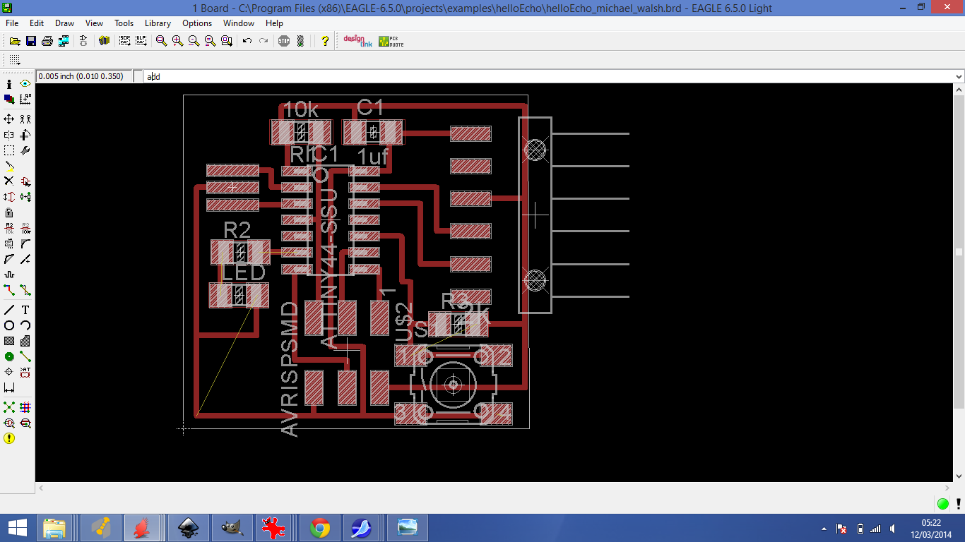
Once all the components had been added to the schematic it was then time to switch to the board layout window. I then moved each part using the move tool and positioned them and used the wire command to connect the parts and make traces between the pads. At this point I did check the design rules options and ensure that the minimum distance between pads and tracks could be milled by the 1/64th inch bit.
When finished my board layout looked like this:
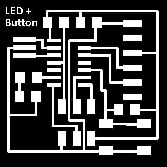
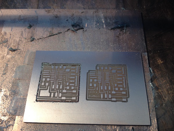
Next I exported the top layer which contained only pads and tracks. I used monochrome and dpi set at 500 as it states in the tutorial which gave me my traces layer. Once exported I viewed the png and it seems to have an extra area of space over on the right hand side of the board that was not being used but was part of the png export. After re-visiting my board layout window I came to the conclusion that the white layer of the FTDI must be making the extra space but I could not find a way of deleting this detail. As a workaround I opened my exported png in Gimp and cropped the image to get rid of this extra area, and whilst in Gimp I decided to label my board with some copper writing as shown below.
*TIP* I found it necessary to use Gimp to do the simple crop and add text function as other programs (Inkscape) seem to mess up the export after the alteration and alter the scale of the board.
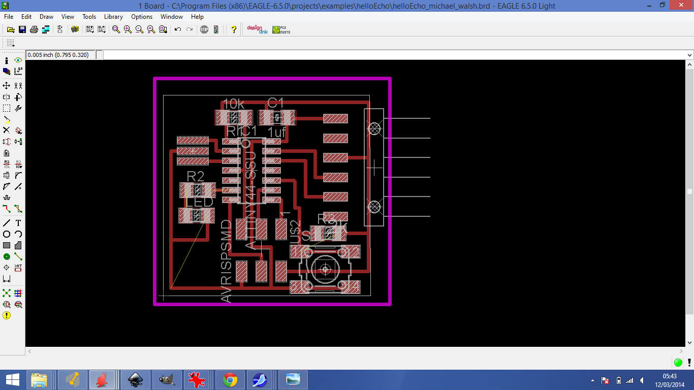
Next I wanted to create a cutout layer or interior as they are labelled in Fab Academy. Firstly I followed the tutorial and tried to export the dimension layer but I couldn't get rid of 2 white circles on the right hand side of the board. As I couldnt seem to delete these elements I decided to make my own cutout layer and use the wire tool to simply draw around the exported top layer as shown below.
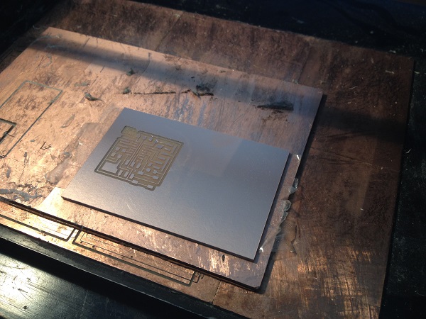
This cutout layer was then exported using the same settings as the traces layer which gave me this.
I checked the exported png size and it seemed to be correct for the traces layer so I was now ready to mill the board.
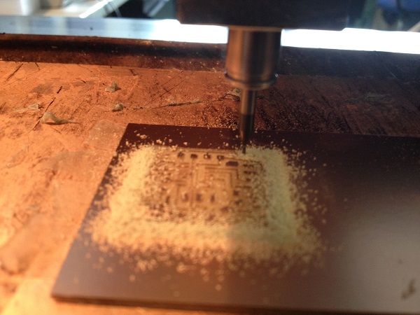
Milling the board
I now feel confident using the modella to mill boards so I followed all the lessons learned when cutting the Fab ISP and set up the machine and milled the traces.
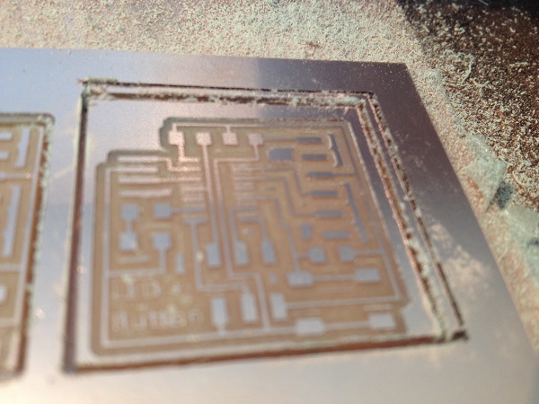
I then milled the cutout layer I had exported and then realised I had a problem. The cutout had cut through the tracks at the top of the circuit and then after checking the png it became more obvious that preserving the white area of the png (as the fab modules are set up to do) means the larger tool (1/32nd inch) cuts inside the line and had been routed through the top of my board. Lesson learned.
I checked my milled board again and although it hadn't cut the traces on the left hand side of the board it was very close to doing so so I decided to open up my cutout layer in all directions to ensure a successfull cut on the second board. This didn't seem to be possible in Eagle as there is a defined origin point for the board layout marked with a white cross which can't be edited. This being the case I then tried to move all parts of my board layout over to allow a wider margin down the left hand side, but the move tool didn't seem capable of this. After getting a bit stuck I decided to make my own work-around by editing the cutout png's size in Gimp to add the extra space in all directions, and reset my cutout origin point 2mm closer to zero (2mm left of my traces path origin).
I then decided I had left too much room on the cutout and re-edited in Gimp to make a smaller cut path and milled it out.This worked well and my second milled board was a success.
Soldering the board
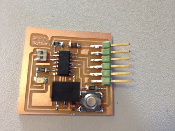
I printed out the board layout and the picture of the board made in the tutorial to help identify the components and their positions on the board. I then soldered each component to the board without much of a problem. The most difficult part to solder on was the 20mHz resonator which has 3 underside connections. This caused me a big problem when I realised that this part was not actually to be used on this board this year and instead a 20Mhz crystal was spec'd out that had a different connection layout. After spending some time trying to de-solder my resonator unfortunately a copper track lifted and became unusable. At this stage I tried to add in some copper vinyl to replace the lifted track and resolder the part and I just about managed it but with all the extra heat ruining through the part it then caused another track to lift and the copper vinyl didn't seem to be adhering to the board. At this point I made the difficult decision to mill a new board. I confirmed that the 20mHz resonator could be used with the embedded programming week and kept the same board layout.
Here is my final milled and soldered board.
Downloadable FIles
LedButton -traces.png
LedButton - cutout.png