This week's summary
This week's exercise was to fabricate and assemble an In System
Programming board using an existing fab lab design.
At a high level, this board (once programmed) allows you to
program other boards that will be made as part of fab lab.
Fabrication Notes
The board was fabricated using the Modela milling
machine.
Traces were cut with a 1/64 inch diameter bit.
The outline was cut using a 1/32 inch diameter bit.
We used the existing settings for speed and depth on the machine.
The material was FR1 which is in effect a 2 layer board.
Traces were cut on one side only.
The material was secured to the bed using double sided tape which
worked well.
Changing the bits is relatively easy but a little tricky at first.
Assembly Notes
I had some prior experience soldering so after a
rocky start I got the hang of it.
It is important to use flux to assist in the flow of solder.
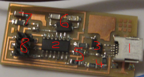
Order of components - USB connector first, IC second, then other
components from center to outside of board (photo at bottom of
page).
Tape the board to the workbench using double sided tape.
I found it useful to tilt the board towards me at approx. 40
degree angle when soldering the USB connector (taped the board to
a piece of bent cardboard).
Don't be afraid to create bridges, they are easily removed using
braided wicking material.
Connections can be checked as you progress using a continuity
meter.
The Outcome
Miraculously, the board worked on first attempt and we were
able to download the program.
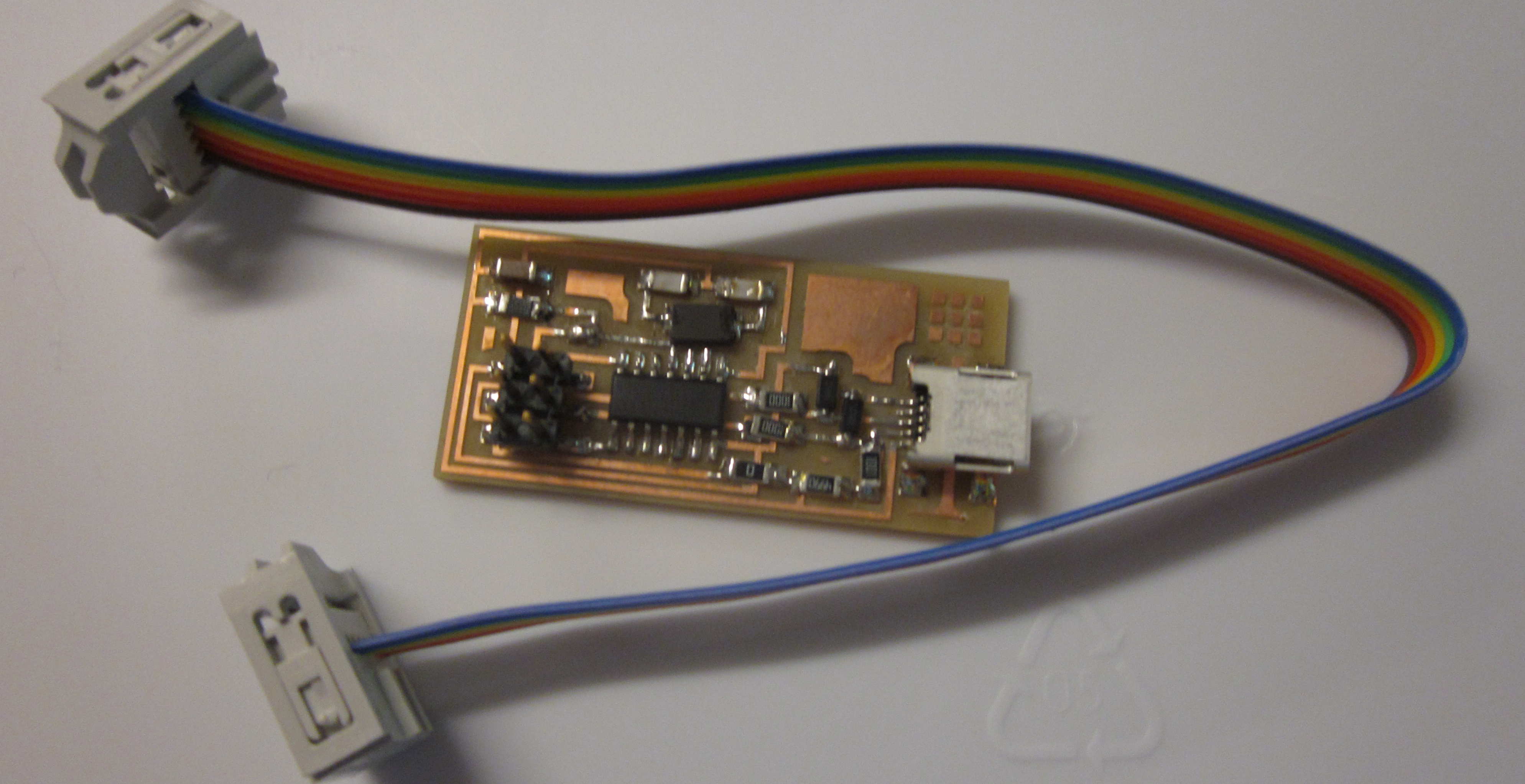
We also built a ribbon cable which is a simple process.
Other Ideas and Reference
For future projects on assembly, we may try to
create a stencil to screenprint solder paste on to the board and
then reflow in an oven.
Challenges
The assembly soldering process was not trivial. I found it best
to follow the order shown below. The USB connector is the hardest
part and you need maximum access to solder it correctly.