This week’s assignment is read a microcontroller data sheet (part 1) and program your board to do something, with as many different programming languages (part 2) and programming environments as possible.
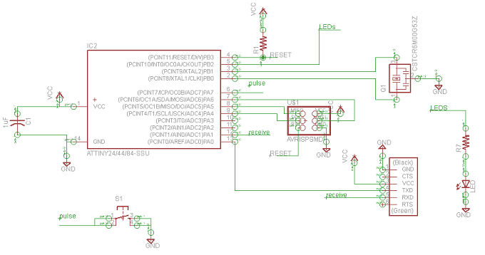
In my case I will use a Atiny44A with the board from electronics design assigment.
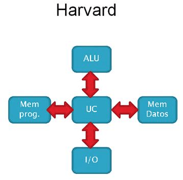
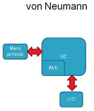
The AVR is a modified Harvard architecture 8-bit RISC single chip microntroller.
It's good to remenber that existe Two architecture in microcontroller:
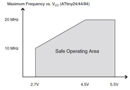
The maximum operating frequency of the device depends on VCC. As shown in Figure, the maximum frequency vs. VCC relationship is linear between 1.8V < VCC < 2.7V and between 2.7V < VCC < 4.5V.
The ATtiny44 features a 10-bit successive approximation ADC. The ADC is connected to 8-pin port A for external sources. In addition to external sources internal temperature sensor can be measured by ADC. Analog Multiplexer allows eight single-ended channels or 12 differential channels from Port A.
The direction of one port pin can be changed without unintentionally changing the direction of any other pin with the SBI and CBI instructions.
All port pins have individually selectable pull-up resistors with a supply-voltage invariant resistance. All I/O pins have protection diodes to both VCC and Ground. The ports are bi-directional I/O ports with optional internal pull-ups.
The driver pin is strong enough to drive LED displays directly.
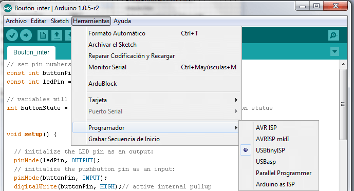
For this part of the assigment, and the use of FABISP programer I need to instal driver for this feature. In my case, the first program was made with Scratch (Ardublock)who need Arduino IDE install.
In this case no problem from input or output name, because I can write directly the configuation pin in the correspondant register.
In this case the Leds is Turn ON when I push the button, in other case the Led is Turn OFF.
But if you decide to use the arduino library, before writing the programation code you can verify what number of tiny pin correspond at the arduino board.
And you write your program.
1) Install AVR studio 6 ( http://www.atmel.com/microsite/atmel_studio6 ).
2) For programming, I am using AVRISPmkII ( http://store.atmel.com/PartDetail.aspx?q=p:10500054 ).
Make sure to power your board from external power supply (USB port with convertor USB to TTL signal)
Steps
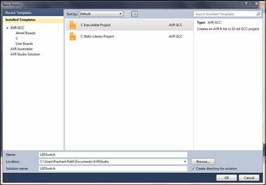
Step 1: Go To File -> New -> C Executable Project (Write name of your project, browse for location). Click OK..
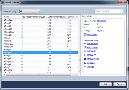
Step 2: In the Device Selection window select your microcontroller. (In my case it is Attiny44A)
Step 3: AVR studio will open up a .c file with some initial code.
You can write you code in this file.
Once finished writing the code, Go to Build - > Build or simple click the Build button shown below.
Step 4: The program will compile your code and if no error you should se Build:1 succeded at the Output window as shown above. A.hex file will be created in the project directory which we have to upload to the micro-controller.
Step 5: Programing the board - Connect the ISP pin of AVRISPmkII to your board (make sure you connect in right polarity). Go to Tools -> AVR programming. In the "Tool" drop-down list select your programmer (I used AVRISP mkII), In Device select your uC ( I used ATtiny44A).
1- Click on "Read" button below Target Voltage, the reading should be the voltage you are supplying to your board (Use external power supply to power your board or in my case a convertor USB to TTL signal, AVRISP mkII do not power the board unlike FabISP).
2- Similarly click on "Read" button below Device ID and your device ID should appear provided all the connections are correct.
Debugging - If something goes wrong, check your connections and try varrying ISP clock speed in the "Interface Settings" Tab.
3-4 For programing go to "Memories" Tab, browse to the projectfolder/Debug and locate the filename.hex file, then click on -"Program" button. If programmed The message at the botton should read like " Programming Flash OK" (5) as shown below..
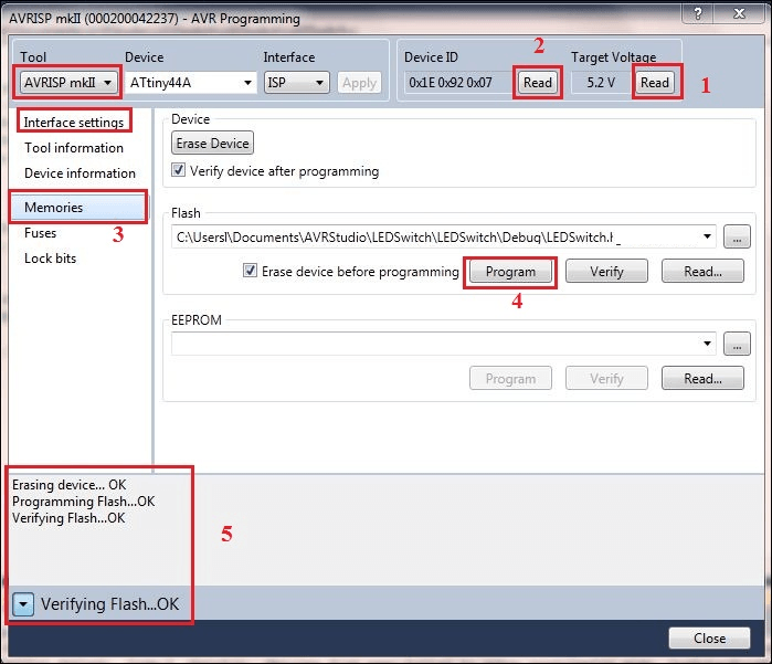
Step 6: Immidiately after the programing finished, the board will start executing the code and we can use the board.
{
// The "special function registers" used in this program are:
// DDRA -- Port A Data Direction Register (DDRB for port B)
// A high (1) value indicates output, low (0) is input.
// We set the 7th bit in DDRA to configure the PA7 pin as output pin.
// PORTA -- Port A Data Register
// This is used to set the output value for each of the eight port A pins.
DDRB = 0b00000100; //Set PB2 (LED) as output pin
PORTB = 0b00000000; //Set output pins in 0v
DDRA = 0b01111111; //Set PA7 (Button) as input pin
PORTA = 0b10000000; //Set PA7 pull-up resistor on
while(1) //Infinite loop
{
if (bit_is_clear(PINA, PINA7)) //If button is pushed (PA7 == 1)
{
PORTB = 0b00000100; // Turn ON the PB2 (LED)
_delay_ms(500); // 500ms
PORTB = 0b00000000; // Turn OFF the PB2 (LED)
_delay_ms(500); // 500ms
}
else
{
PORTB = 0b00000100; // Turn ON the PB2 (LED)
}
}
return 0;
}
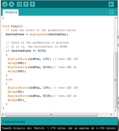
Blink LED, and when you push the button the led stop blinking
click on picture to see the video
That's all ....
Part 1
Read a microcontroller data sheet.In my case I will use a Atiny44A with the board from electronics design assigment.
Atiny44A specification
The AVR is a modified Harvard architecture 8-bit RISC single chip microntroller.
It's good to remenber that existe Two architecture in microcontroller:
 |
 |
| 8-Bit Microcontroller Advanced RISC Architecture |
- 120 Powerful Instructions - 32 x 8 General Purpose Working Registers. |
I/O and Packages | - Available in 14-Pin SOIC and PDIP - Twelve Programmable I/O Lines |
| Non-Volatile Program and Data Memories | - Program Memory Flash of 2/4/8K Bytes (Endurance: 10,000 Write/Erase Cycles) - Programmable EEPROM of 128/256/512 Bytes (Endurance: 100,000 Write/Erase Cycles) - Internal SRAM of 128/256/512 Bytes (Data Retention: 20 years at 85°C / 100 years at 25°C - Programming Lock for Self-Programming Flash & EEPROM Data Security) |
Special Microcontroller Features | - Debug WIRE On-chip Debug System - In-System Programmable via SPI Port - Internal and External Interrupt Sources: Pin Change Interrupt on 12 Pins - Internal Calibrated Oscillator - On-chip Temperature Sensor |
| Peripheral Features | - One 8-Bit Timer/Counter with Two PWM Channels - 10-bit ADC - Universal Serial Interface |
Speed Grade | - ATtiny44V 0 – 4 MHz @ 1.8 – 5.5V 0 – 10 MHz @ 2.7 – 5.5V - ATtiny44 0 – 10 MHz @ 2.7 – 5.5V 0 – 20 MHz @ 4.5 – 5.5V |
| Operating Voltage: | 1.8 – 5.5V for ATtiny44V 2.7 – 5.5V for ATtiny44 |
Industrial Temperature Range: -40°C to +85°C Low Power Consumption |
- Active Mode (1 MHz System Clock): 300 μA @ 1.8V - Power-Down Mode: 0.1 μA @ 1.8V |
The maximum operating frequency of the device depends on VCC. As shown in Figure, the maximum frequency vs. VCC relationship is linear between 1.8V < VCC < 2.7V and between 2.7V < VCC < 4.5V.
| Serial Programming: Both the Flash and EEPROM memory arrays can be programmed using the serial SPI bus while RESET is pulled to GND. The serial interface consists of pins SCK, MOSI (input) and MISO (output); | 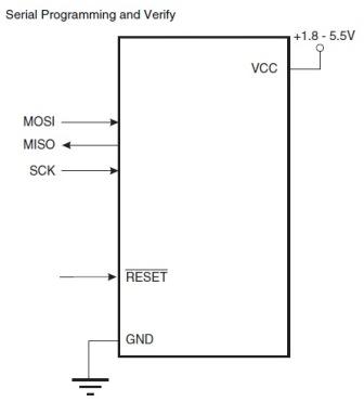
|
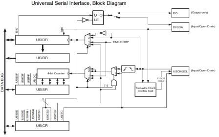
| The Universal Serial Interface (USI), provides the basic hardware resources needed for serial communication. Combined with a minimum of control software, the USI allows significantly higher transfer rates and uses less code space than solutions based on software only. Interrupts are included to minimize the processor load. A simplified block diagram of the USI is shown in figure. |
|
The ATtiny44 features a 10-bit successive approximation ADC. The ADC is connected to 8-pin port A for external sources. In addition to external sources internal temperature sensor can be measured by ADC. Analog Multiplexer allows eight single-ended channels or 12 differential channels from Port A.
The direction of one port pin can be changed without unintentionally changing the direction of any other pin with the SBI and CBI instructions.
All port pins have individually selectable pull-up resistors with a supply-voltage invariant resistance. All I/O pins have protection diodes to both VCC and Ground. The ports are bi-directional I/O ports with optional internal pull-ups.
The driver pin is strong enough to drive LED displays directly.
Part 2
Program your board to do something, with as many different programming languages and programming environments as possible.For this part of the assigment, and the use of FABISP programer I need to instal driver for this feature. In my case, the first program was made with Scratch (Ardublock)who need Arduino IDE install.
- Download the Arduino 1.05-r02 ,
- Installing ATtiny board support in Arduino
Download: ATtiny (from this GitHub repository)
Locate your Arduino sketchbook folder (you can find its location in the preferences dialog in the Arduino software)
Create a new sub-folder called "hardware" in the sketchbook folder.
Copy the attiny folder from inside the .zip to the hardware folder.
Restart the Arduino development environment.
You should see ATtiny entries in the Tools > Board menu.
.
and FTDI drivers - You need to install the driver for fabISP programmer for that you download usbtinyisp_libusb-win32_1.2.1.0.zip and install the driver
- Connect the cable between the fabISP programmer, the echo hello board, the miniUSB from the fabISP and the computer and finally the FTDI connector from the echo hello board and the computer
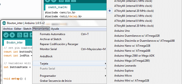
- Select the "ATtiny44(external 20 Mhz clock) from the tools menu Now all is ready to begin the programation
Ardublock with arduino IDE
- if you've never program, it is easier to start with the "Scratch" (here ardublock) programming system designed by MIT so they can start coding children from 8 years.
- In this case you can download ArduBlock (http://cloud.github.com/downloads/taweili/ardublock/ardublock-all.jar)
- Include all.jar ardublock-file in the tools folder of the Arduino IDE ".... / arduino-1.0.5-r2\tools\ArduBlockTool\Tool\ ardublock-all.jar" You must create folders: ArduBlockTool\Tool\
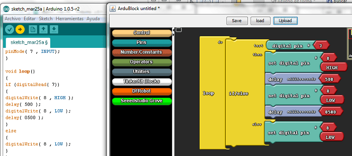
after programing using the block you click to upload button and the program is transform to "C" code and program the board.
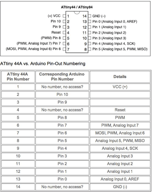
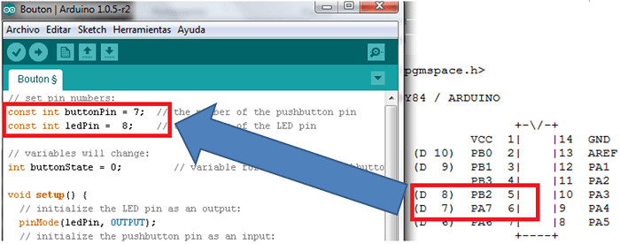
The First program don't work...and I did not understand that until check-documentation again comparing it with arduino Atiny44v. At that moment I realized that the arduino pin numbers correspond to the board, not the component. In the figure below we see the correspondence between the card and the Tiny44V component. I applied and everything worked.
Arduino IDE
Programing the tiny board is easy if you know "C" language. The first program that I can make is :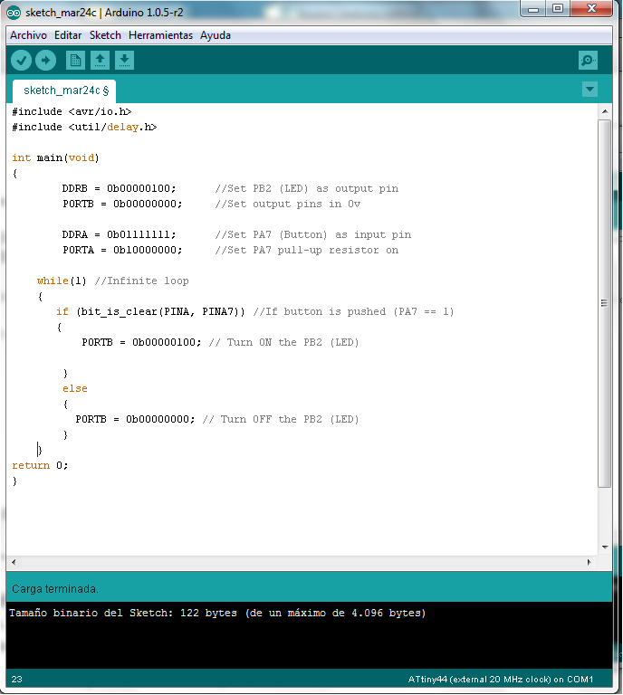
In this case no problem from input or output name, because I can write directly the configuation pin in the correspondant register.
In this case the Leds is Turn ON when I push the button, in other case the Led is Turn OFF.
But if you decide to use the arduino library, before writing the programation code you can verify what number of tiny pin correspond at the arduino board.
And you write your program.
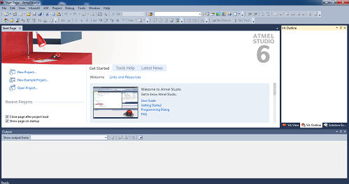
AVR Studio
1) Install AVR studio 6 ( http://www.atmel.com/microsite/atmel_studio6 ).
2) For programming, I am using AVRISPmkII ( http://store.atmel.com/PartDetail.aspx?q=p:10500054 ).
Make sure to power your board from external power supply (USB port with convertor USB to TTL signal)
Steps
Step 1: Go To File -> New -> C Executable Project (Write name of your project, browse for location). Click OK..
Step 2: In the Device Selection window select your microcontroller. (In my case it is Attiny44A)
Step 3: AVR studio will open up a .c file with some initial code.
You can write you code in this file.
Once finished writing the code, Go to Build - > Build
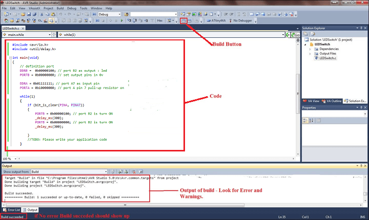
Step 4: The program will compile your code and if no error you should se Build:1 succeded at the Output window as shown above. A
Step 5: Programing the board - Connect the ISP pin of AVRISPmkII to your board (make sure you connect in right polarity). Go to Tools -> AVR programming. In the "Tool" drop-down list select your programmer (I used AVRISP mkII), In Device select your uC ( I used ATtiny44A).
1- Click on "Read" button below Target Voltage, the reading should be the voltage you are supplying to your board (Use external power supply to power your board or in my case a convertor USB to TTL signal, AVRISP mkII do not power the board unlike FabISP).
2- Similarly click on "Read" button below Device ID and your device ID should appear provided all the connections are correct.
Debugging - If something goes wrong, check your connections and try varrying ISP clock speed in the "Interface Settings" Tab.
3-4 For programing go to "Memories" Tab, browse to the projectfolder/Debug and locate the filename.hex file, then click on -"Program" button. If programmed The message at the botton should read like " Programming Flash OK" (5) as shown below..
Step 6: Immidiately after the programing finished, the board will start executing the code and we can use the board.
Code
int main(void){
// The "special function registers" used in this program are:
// DDRA -- Port A Data Direction Register (DDRB for port B)
// A high (1) value indicates output, low (0) is input.
// We set the 7th bit in DDRA to configure the PA7 pin as output pin.
// PORTA -- Port A Data Register
// This is used to set the output value for each of the eight port A pins.
DDRB = 0b00000100; //Set PB2 (LED) as output pin
PORTB = 0b00000000; //Set output pins in 0v
DDRA = 0b01111111; //Set PA7 (Button) as input pin
PORTA = 0b10000000; //Set PA7 pull-up resistor on
while(1) //Infinite loop
{
if (bit_is_clear(PINA, PINA7)) //If button is pushed (PA7 == 1)
{
PORTB = 0b00000100; // Turn ON the PB2 (LED)
_delay_ms(500); // 500ms
PORTB = 0b00000000; // Turn OFF the PB2 (LED)
_delay_ms(500); // 500ms
}
else
{
PORTB = 0b00000100; // Turn ON the PB2 (LED)
}
}
return 0;
}
Blink LED, and when you push the button the led stop blinking
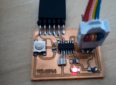
click on picture to see the video
That's all ....