
Classes > Electronics Design
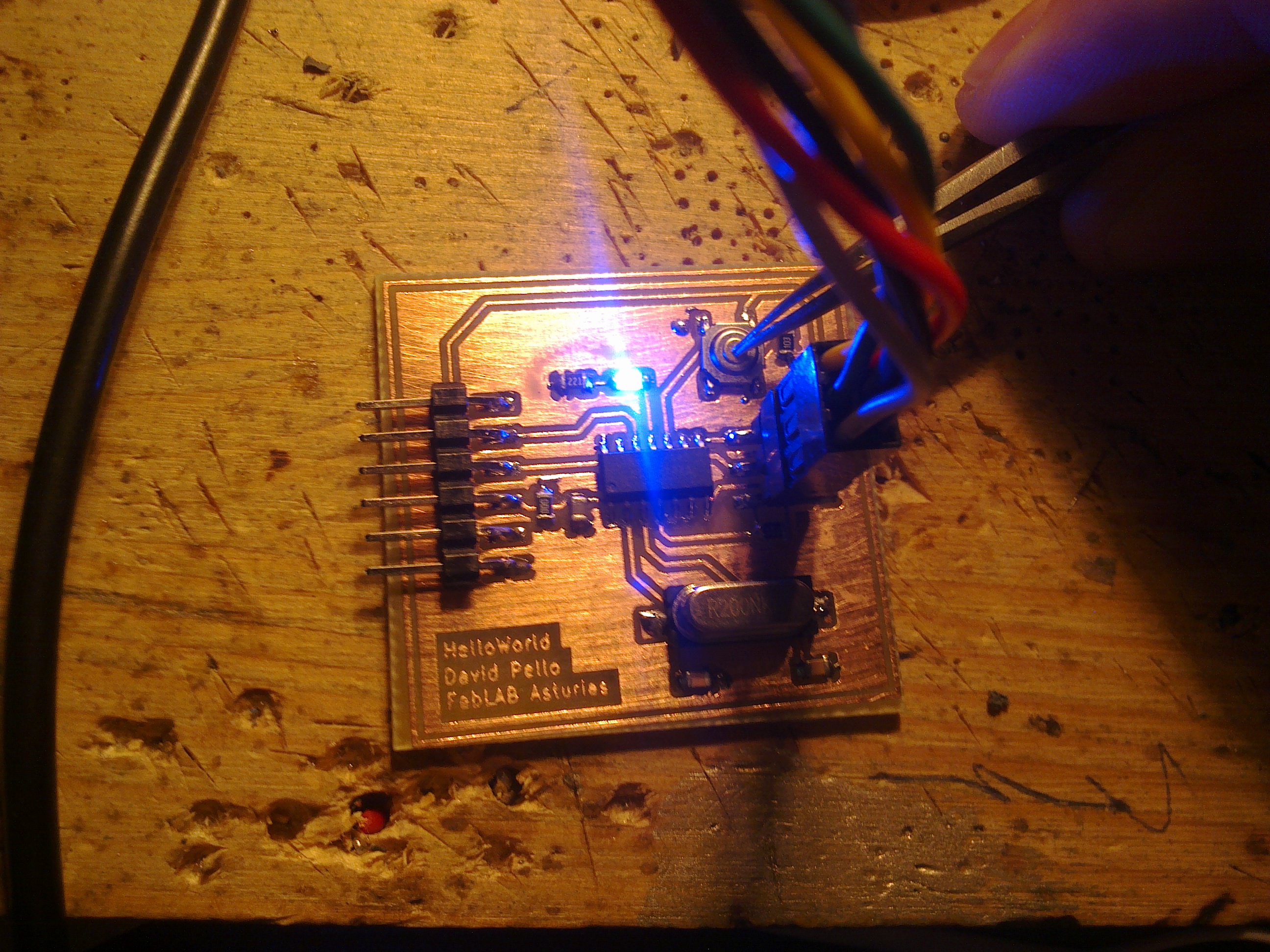
This week we had to modify the "hello world" mcu board. This board is a small PCB with an attiny44, ftdi and isp headers, and some passives for the reset circuit and bypass. We had to add a LED and a momentary switch to it, build it and test it.
The tool I choosed for this task is Kicad. Kicad is a really nice open/free-software EDA package, that includes schematic capture, pcb design, CAM process and library editor. I have been using Kicad for a while, and I feel really confortable using it. I used Eagle before, and it's also a nice tool, but after using Kicad without the limitations of the free Eagle version, going back to Eagle feels like a step back.
So first I started capturing the schematic of the hello world board, looking at the connections of the given PCB drawing. As it is a really simple board this was an easy task. After this, I drawed the schematic in kicad.
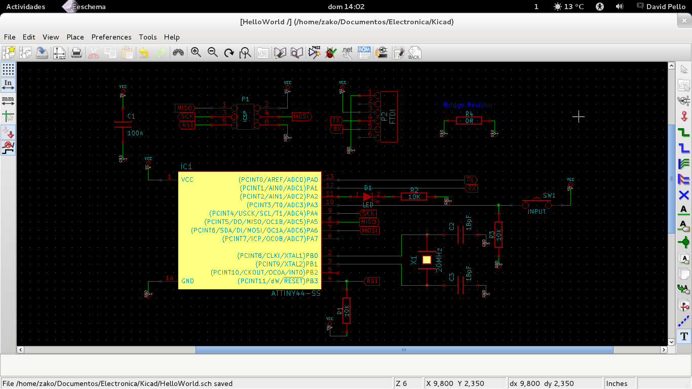
I had to add some components to the Kicad library, the FTDI and ISP SMD headers, and the SMD tactile switch. The library editor of Kicad is really easy to use, so looking at the datasheets and at the Eagle parts, I got them ready in no time.
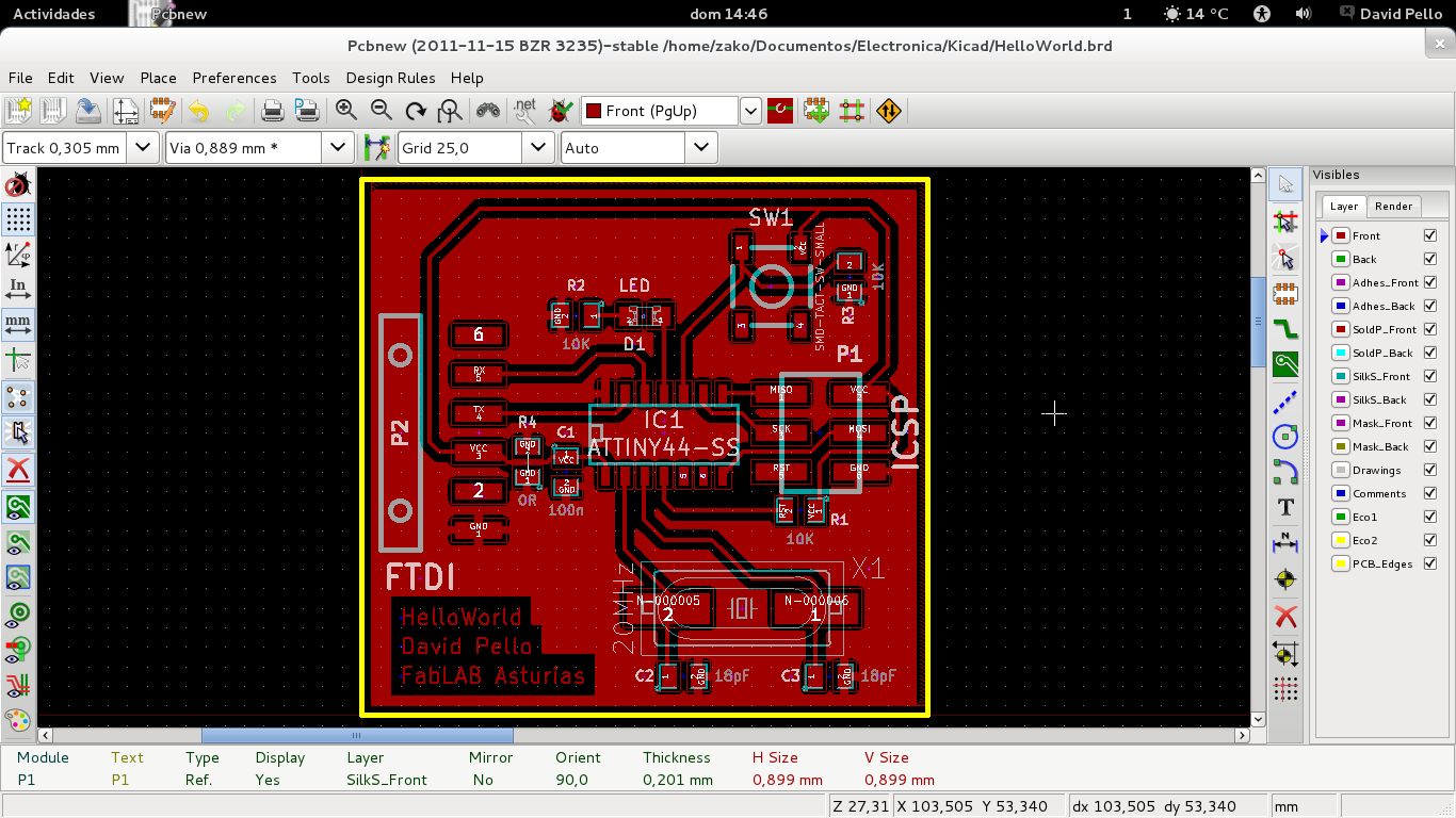
Then I started designing the PCB. After placing the components and doing most of the tracks, I couldn't route the ground between two isolated places, so I used a 0 Ohm resistor to make a bridge, and the board was finished.
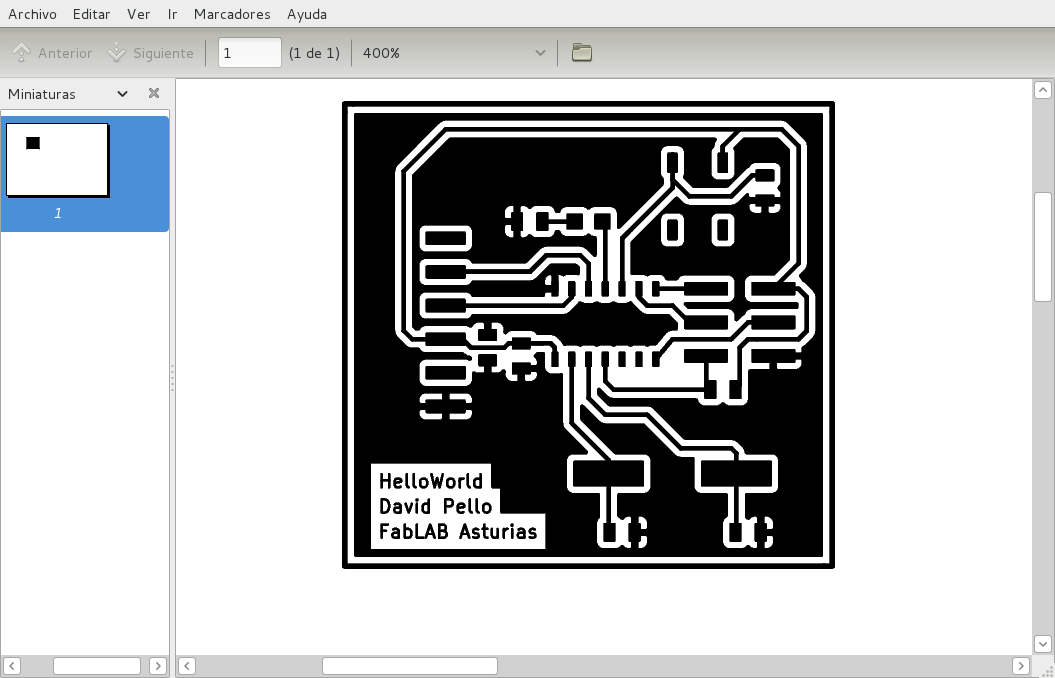
After this I used the Plot function of kicad to get a postcript of the top layer, with this I can print it on tracing paper to do the UV method, or the tonner-transfer method, or milling the board, or whatever.
The Kicad files for the schematic and PCB, here:
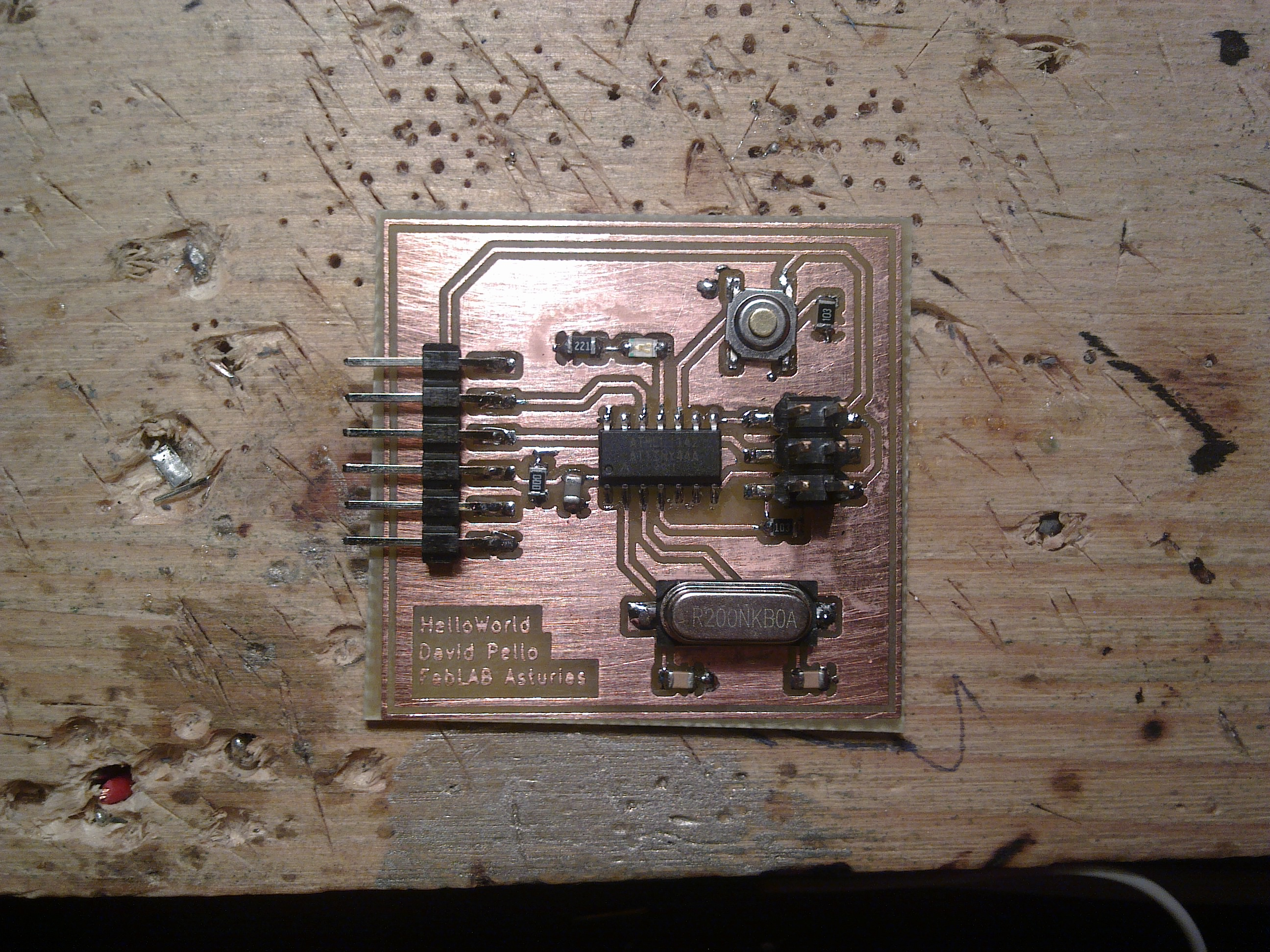
Then I made the PCB, soldered the components, and wrote a simple assembler program to test it. The program reads the button and lights the LED when pressed. It's written with the avra assembler.
Program files:
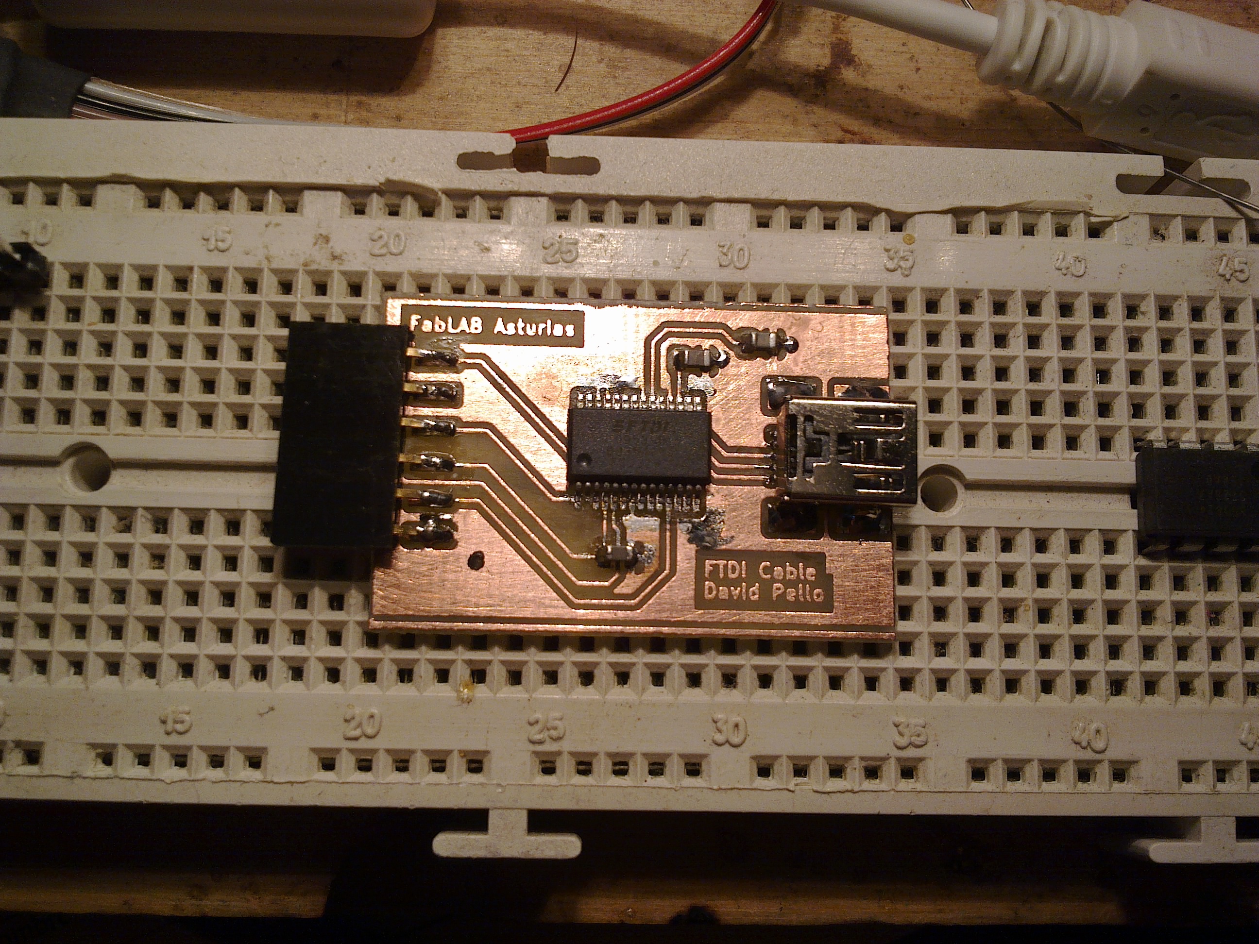
As an extra assignment I wanted to design also my own ftdi cable. It's based on the ft232r reference design, just the USB port, some decoupling capacitors, and the FTDI header.
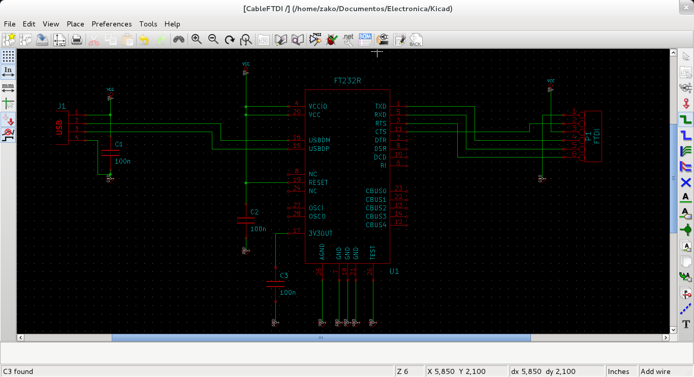
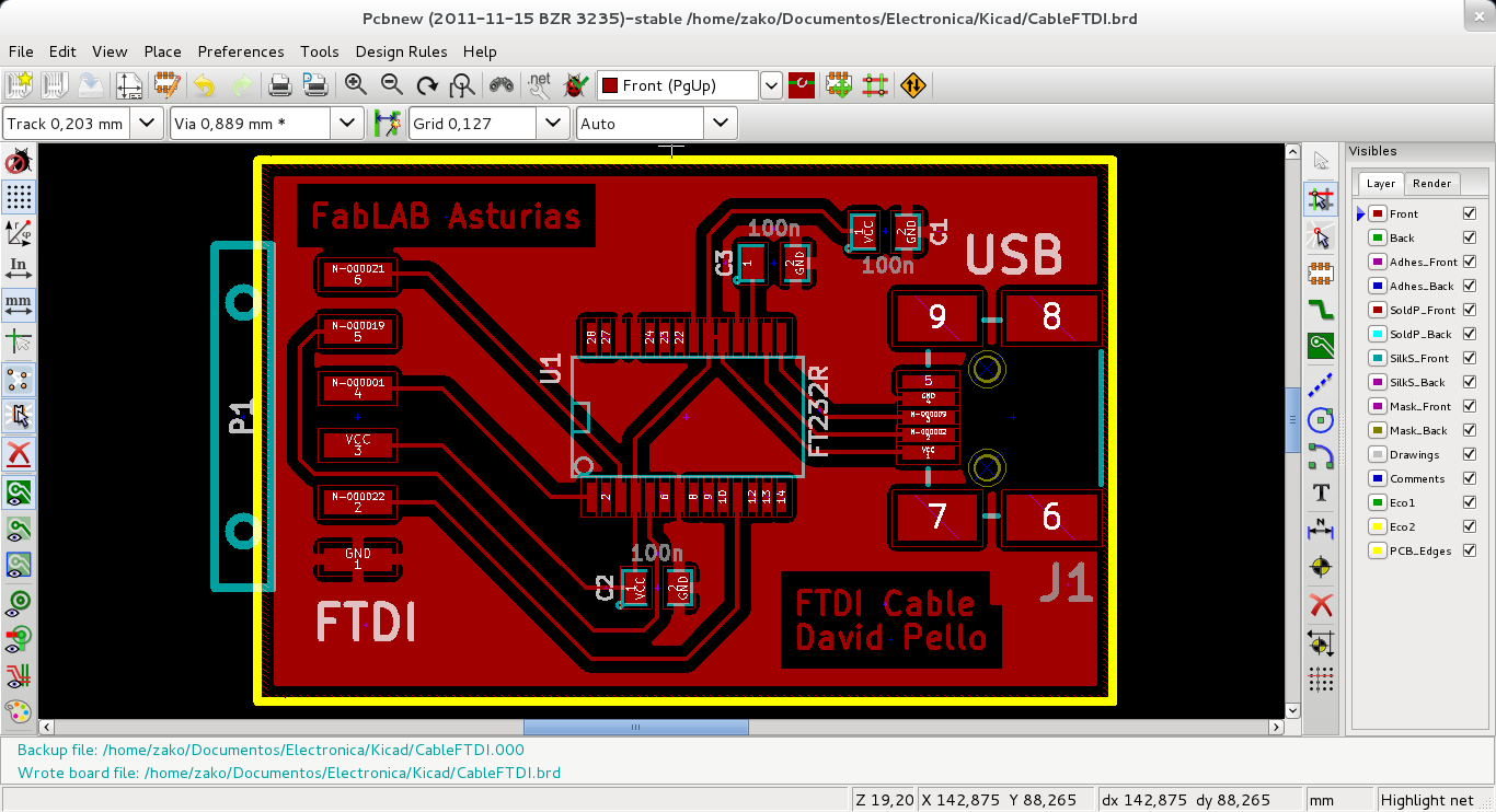
The Kicad files for the FTDI DIY cable, here: