Additional Images and Videos of this project are on my tumblr blog:
part1 part2 part3 part4 part5 video of CNC milling
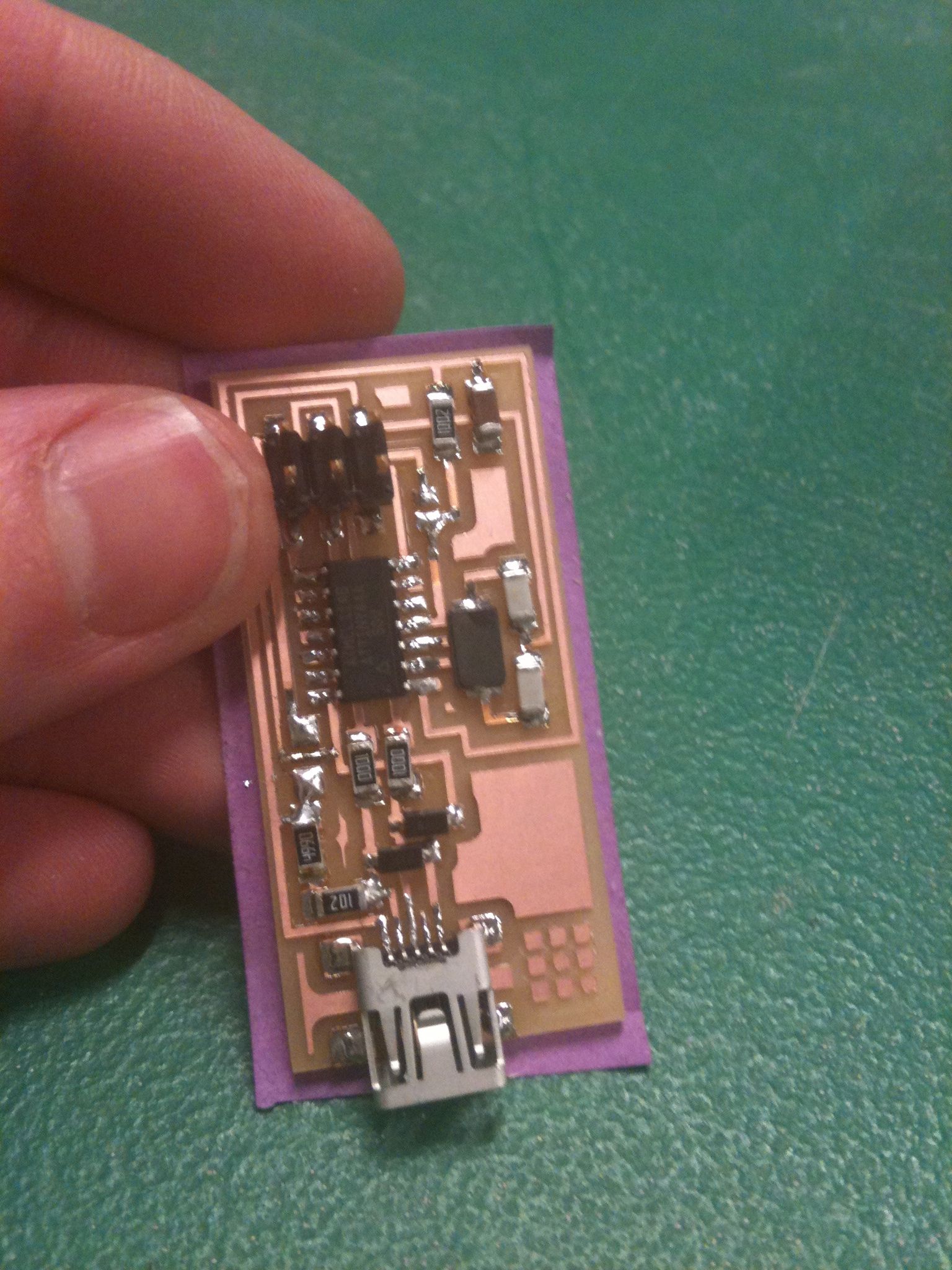
This week we had a very specific assignment with very specific steps to follow. To be perfectly honest, I don't actually understand what we made or how it works, but I suspect it will play into future lessons somehow. We built a device called the Fab ISP Programmer, which to my untrained eyes and brain is a circuit board with a mini USB port on it.
The first step to making this board was to mill out the actual circuit pattern using a CNC milling machine. The material we used consisted of a layer of copper laminated onto a layer of nonconductive material (plastic I think). The CNC milling machine is a small rotary bit toolhead which can move on the x, y, and z axis. The unmilled laminate board is mounted in the bed of the machine using double-sided tape. To make the circuit pattern, you download the design from the Fab Academy website, load it into the machine, and run the machine. The small spinning mill bit cuts through the copper layer and into the inert material below, carving channels in the board and eventually leaving only a series of interconnected lines of copper on the surface. These lines of copper will conduct current between the various elements on the board.
The second step involves soldering all the components onto the board. This is called "stuffing" the board, and the placement and selection of components is determined by the schematic available on the Fab Academy website. There are transistors, capacitors, resistors, diodes, a crystal, an actual chip called "attiny44a", and a mini USB header. All of these pieces are soldered onto the board using tin solder. In addition to the components, there are two solder "bridges" which temporarily link different parts of the boards to each other. These bridges are used to load the initial firmware onto the board, and then must be removed afterwards in a second soldering operation. More on this later. Maybe.
The actual soldering method is pretty easy provided you prep your workspace properly. One thing that helped me was to raise the work surface closer to eye level by setting a small footstool on top of the table and using it as my work surface. The soldering is done with a tin-based solder and an electrically hearted soldering Iron, set to 700 degrees Fahrenheit. The method that worked best for me was to dip the end of my solder wire into the flux gel so that there's just a tiny bit on the tip, then touch the heated element of the iron to the area of copper I wanted to solder to heat it up. While the copper is heating up, I tentatively tap the end of the solder wire onto the surface so that some of the flux flows off of the solder wire and onto the copper surface. As the copper heats up, the flux liquifies and spreads across the copper. When the copper is at just about the right temperature, the flux will start to smoke a tiny tiny bit, which is when I touch the tip of the solder wire to the surface a second time and if I'm lucky a tiny bit of it will flow onto the copper. If it doesn't flow, I can touch it directly to the tip of the soldering iron, and it will usually bind partially to the copper and partially to the soldering iron. I then remove the soldering iron and use a damp sponge to wipe off any excess solder still clinging to the tip.
Once this initial dab of solder is in place, a component (such as a resistor, capacitor, etc) can be laid down on top of it and held in place with tweezers while the soldering iron is placed onto the connection point which raises the temperature of the solder and causes it to flow out from under the component and bind the component to the copper.
I don't know anything about electronics, so this whole process quickly turned into a game of matching colors and shapes. I looked at the sample boards and the images on the website, and then rummaged through our local Fab Lab's box of components until I found pieces that looked like the ones in the example. Then I soldered them into the corresponding spots on my own board. Once everything was in place, I plugged the Fab ISP into my computer's USB port. The fact that no smoke issued from the device, and no error messages appeared on my computer, were indication enough that I was at least somewhat on the right track.
The next few steps involved installing and running specific software on my computer from the command line. Fortunately the instructions worked exactly as they were supposed to and there were no hiccups.
To install the firmware, I had to connect a second device to my computer, which would in turn be connected to the Fab ISP. The device I used was a black box with a 6 pin connector called a "USBtiny programmer".
From there, it was just another series of steps involving typing various codes into the command line on my computer. This was supposed to allow a program called "make" to install firmware on the FabISP. Everything worked fine up unitl the last step, when I received an error message.
Well, it turns out my matching of colors and shapes didn't serve me all the way through this project after all. Remember earlier when I mentioned the solder bridges? They are used to load the firmware, and then once the firmware is loaded, they are removed from the boards Well, since all of the example boards are *finished* boards, they of course do not have the solder bridges on them anymore, which meant that when I replicated them in the apelike fashion that is my wont, the board I built did not have solder bridges. Which in turn meant that my board in its initial form could not be loaded with the firmware, which in its own turn lead to the error message I received.
So: FINE. I'll READ.
After scanning back through the instructions I found the entry about the solder bridges. I set up my soldering station a second time, and bridged the two areas specified on the diagram. Then I connected the FabISP back to my computer and ran the steps again. It worked this time.
The final step, once the FabISP had been programmed, was to remove the solder bridges. Unfortunately this is not something that I got to see a demo of in class so I pretty much had to guess how to do it. I had overheard other students talking about using a woven rope of fine copper wire to "wick" the solder off of the board, but had not seen it demonstrated. I should mention at this point that I was working on this project fairly late at night when no-one else was in the lab, so there was nobody available to ask about this.
After some fudging around with the copper braid and the soldering iron, I managed to remove a little bit of the solder. It didn't look pretty, and probably a lot more of the solder could have been removed, but it was enough to eliminate the bridge so that the two areas of copper were no longer connected. Good enough for me.
I was initially stressed out about this project because it seemed very technical and involved, plus this week brought with it many outside obligations and deadlines such that I did not expect I would have time to finish the FabISP. However once I realized that it was not necessary to actually *understand* any of the concepts or processes I was using, it became a simple matter of following basic steps.
Here is an image of the completed fabISP: