6. Electronics Design
This week I learned how to use KiCad to create electronic circuit schematics and PCB boards.
Research
Prior to this experience, I haven't worked with KiCad at all I didn't even know that PCB boards were even manufactured this way. Honestly, I didn't even know anything about making circuits at all.
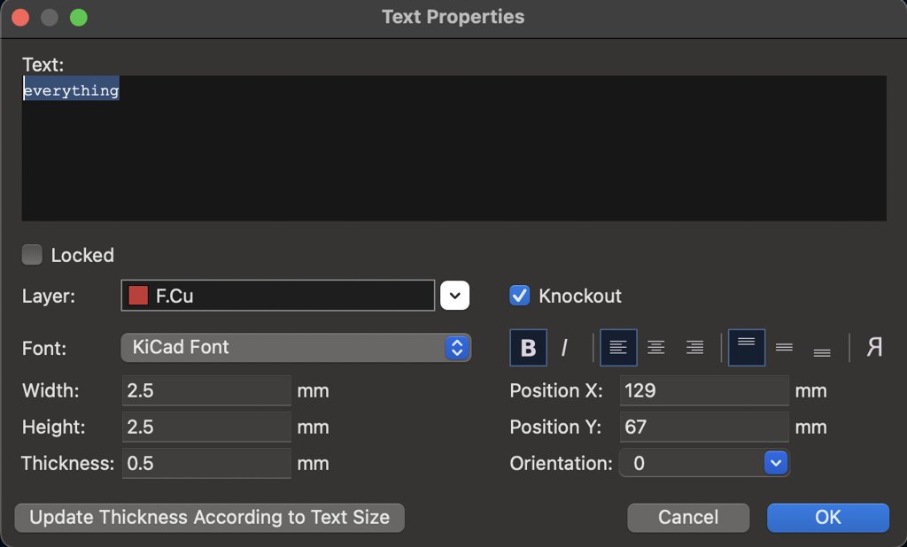
But I do like bagels.. everything bagels to be exact...

Setting up KiCad
For this week we needed to learn and use a Electronic design automation (EDA) tool to design a circuit board. Downloading KiCad had it's own set of struggles. I was having some problems with organizing my files. I first downloaded KiCad for Mac from the website and I moved it to my applications folder.
From here I had to download the Fab Academy library. What? Well, basically in KiCad is a catalog of materials and circuit stuff, but of course it doesn't have everything. Part of the Fab Academy catalog is a list of equiptment most labs have, so the library that I was trying to download would showcase the rest of those parts. This means I would be able to design a board I would be more likely to be able to produce.
On the Fab Academy home site, the inventory is showcased here.
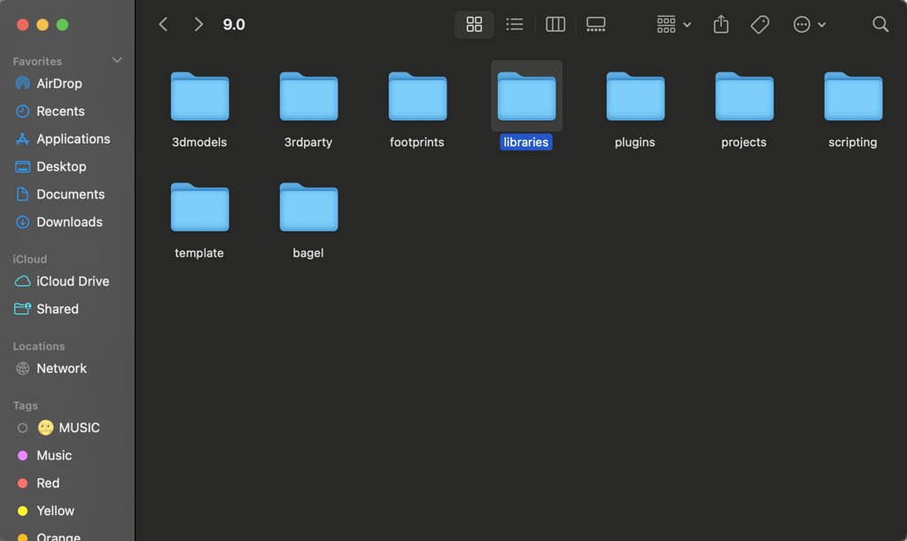
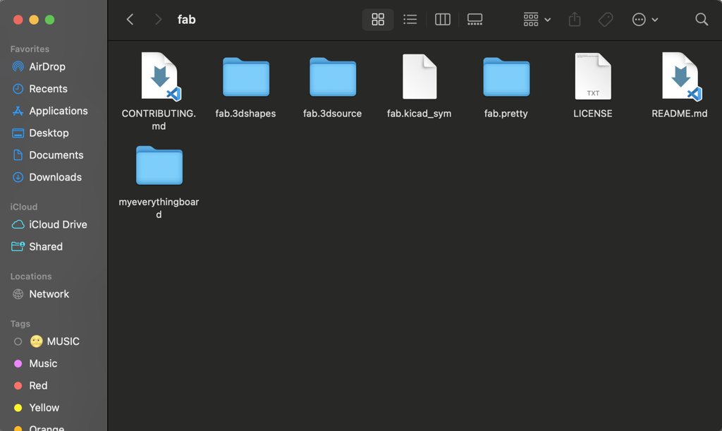
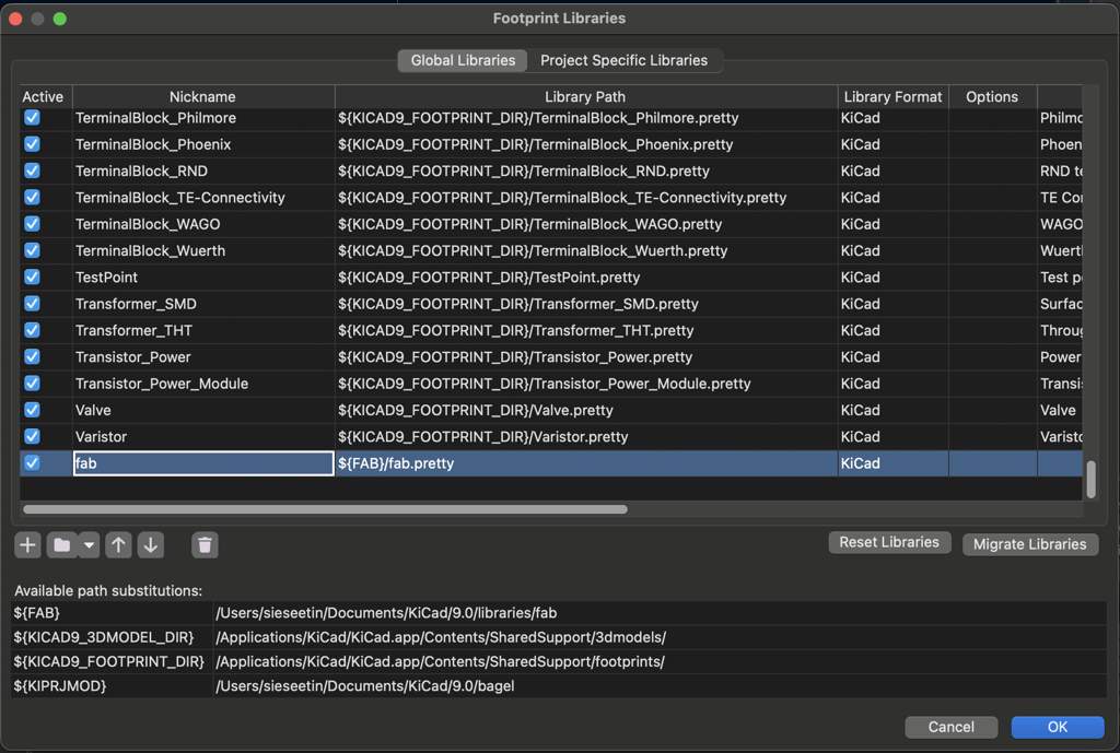
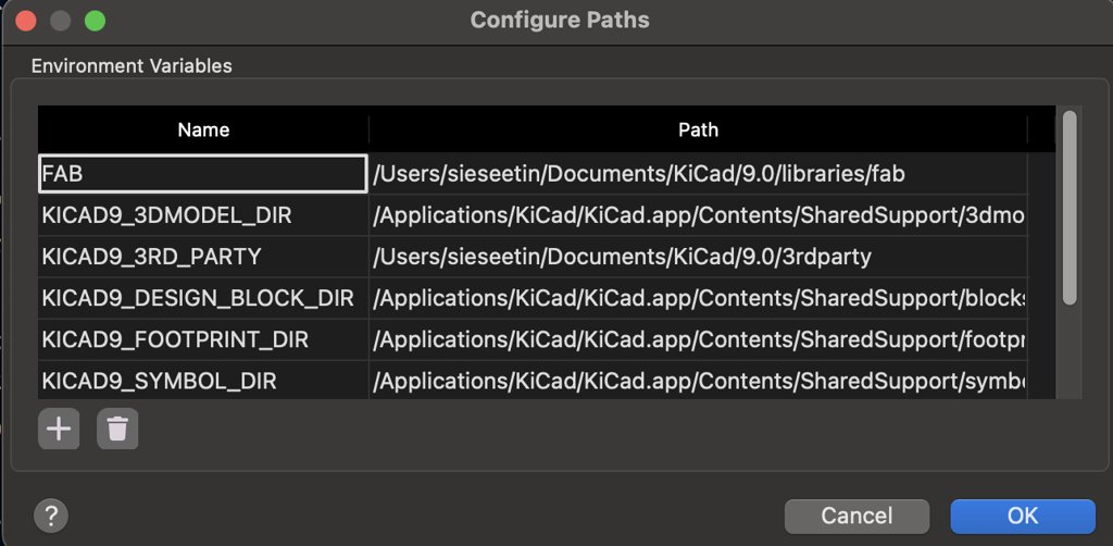
To download KiCad, I followed a tutorial. First, I downloaded KiCad from the official website onto my computer. Then I downloaded the Fab Academy folder and renamed it to 'fab'. I then created a 'libraries' folder inside of KiCad -> 9.0, and then dragged the new 'fab' folder inside 'libraries'.
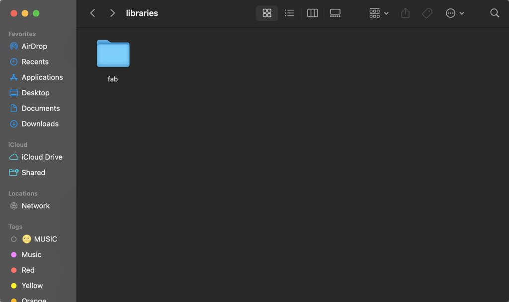
I connected the symbol libraries and footprint libraries from that folder to my version of KiCad.
And just like that, the download was done!
Creating a Design
Now that KiCad is all set up, I need to create a circuit board. What!? How do I even do that?! I can't even spell circut.
No fear. I can rest easy, leaning on the shoulders of fab academy documentors who came before me.
• • • Schematic Editor
I started playing around in the schematic editor, which is the inital phase that Kicad will start you on when you first start a new project. It's basically a rough draft that doesn't account for scale or layout of the components, but just helping you understand and test the logic of your pieces.
This icon will open the panel in which you can add components to your design.

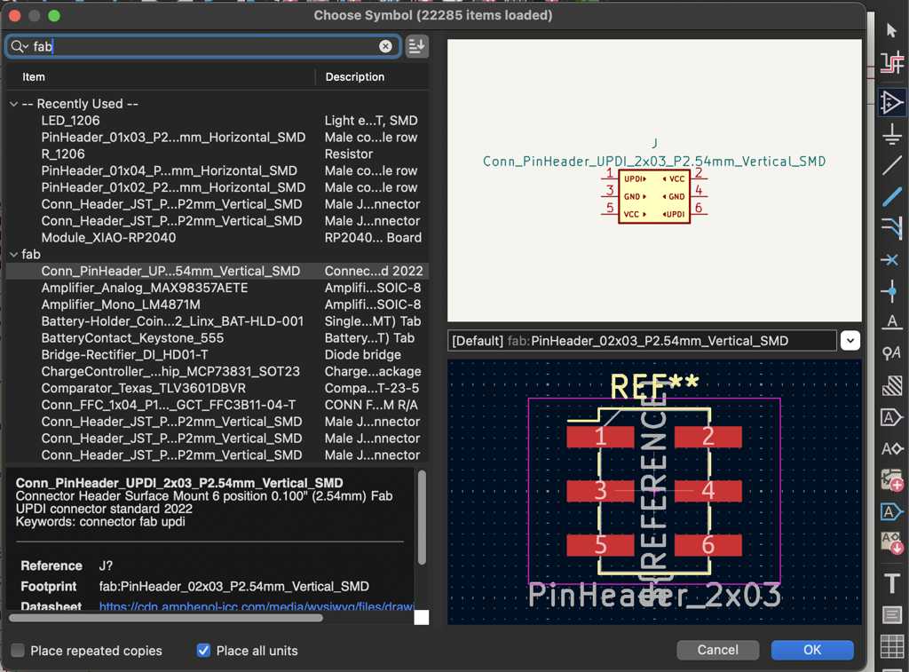
When I open this menu and select items I always make sure to preface my search with 'fab' so only components that I know my Fab Lab will have will be displayed. This makes it a lot easier to coordinate with my lab's inventory so when it gets down to making the board I have everything (bagel).
This icon controls the wiring tool, which is essential for connecting together parts on your schematic. I learned it was totally OK to get messy with the placement and wiring in the schematic stage; it's really just acting as a guide for yourself and well as an outline for the PCB version which actually counts.

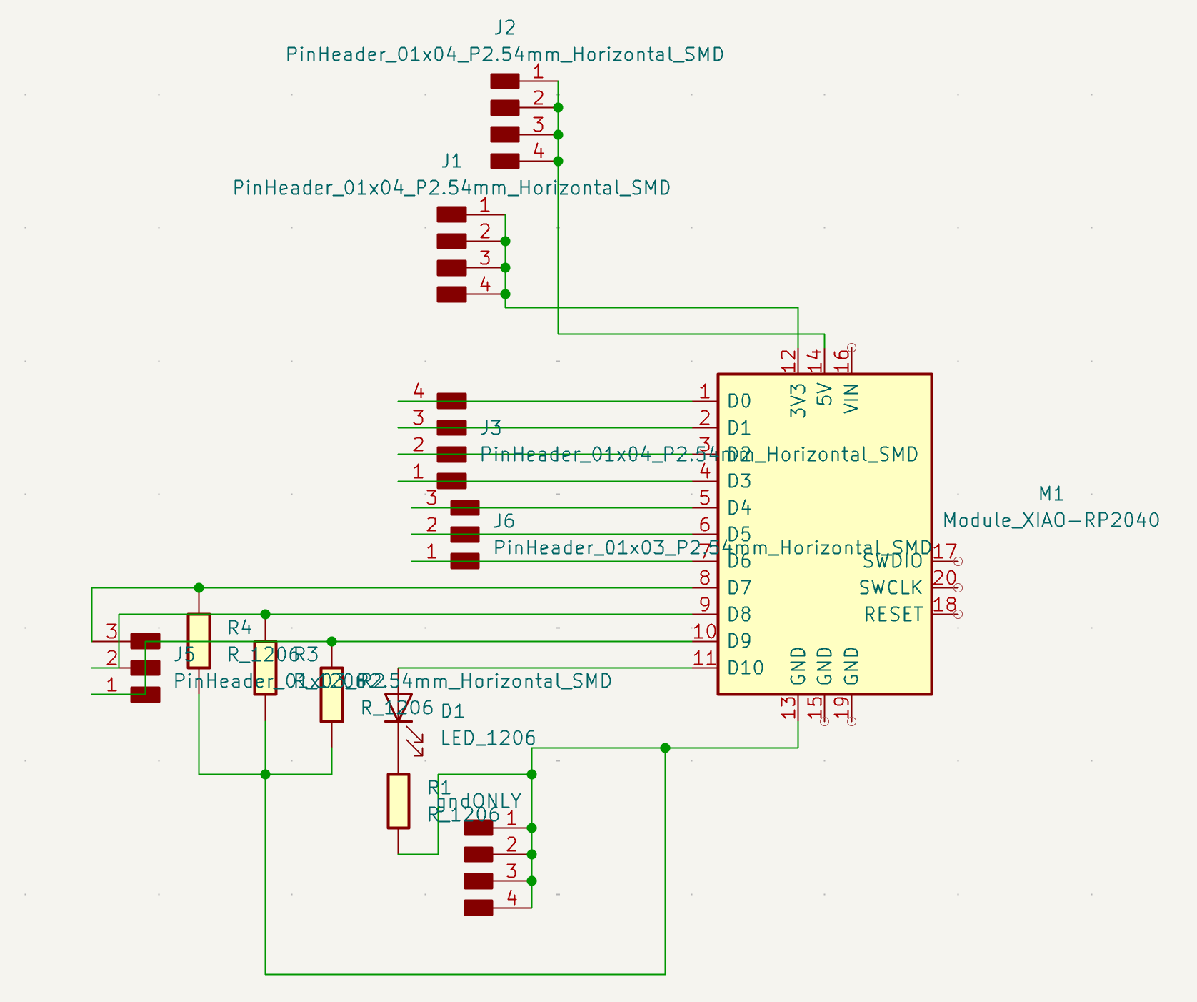
This was my final schematic!
Download Schematic
• • • PCB Design
Truth hurts. PCB layout does too. No more fooling around in the light airy spacey world of KiCadia's Schematic-andia. NO! Now we are in PCB City with nothing but a tattered plan and a dream. Let's go for it...
First, we need to bring over the plan we created in the schematic editor. You can do this by clicking this icon.

This menu will appear. It's explaining what is coming over from the schematic. If you choose to go back and update your schematic once you've already begun your PCB layout, this menu will help show you what are the new components coming over and what you already have placed.
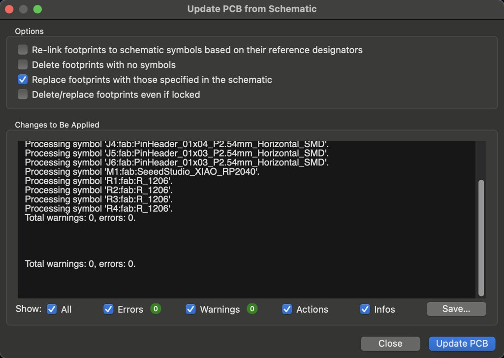
Click 'Update PCB'. Now all those parts are in. They're going to appear clustered together as a big blob of red and blue lines. Place this in the middle of the PCB editor. Now you can start to space out the pieces to your liking, and to think about how your board will look like in real life.
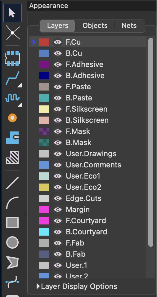
The side panel is where you can add and change elements on your main workspace. The F.Cu layer contains all of the traces that will be cut when you export your board. This is where you’ll get the plots and pads that the program generates based on the electronic components you're using. You can also use the jagged blue line tool to add wire paths for connecting different components—these are the traces that you board will move power along.
On the Edge.Cuts layer, this is where your board will actually be cut out from the PCB. You can create an organic shape, or use the rectangle or circle tools to define the shape of your board. Keep in mind that when you're drawing your edge cut, it needs to be large enough to act as the base of your board—make sure it's bigger than the components you're using and that it includes all the traces you drew on your F.Cu layer.
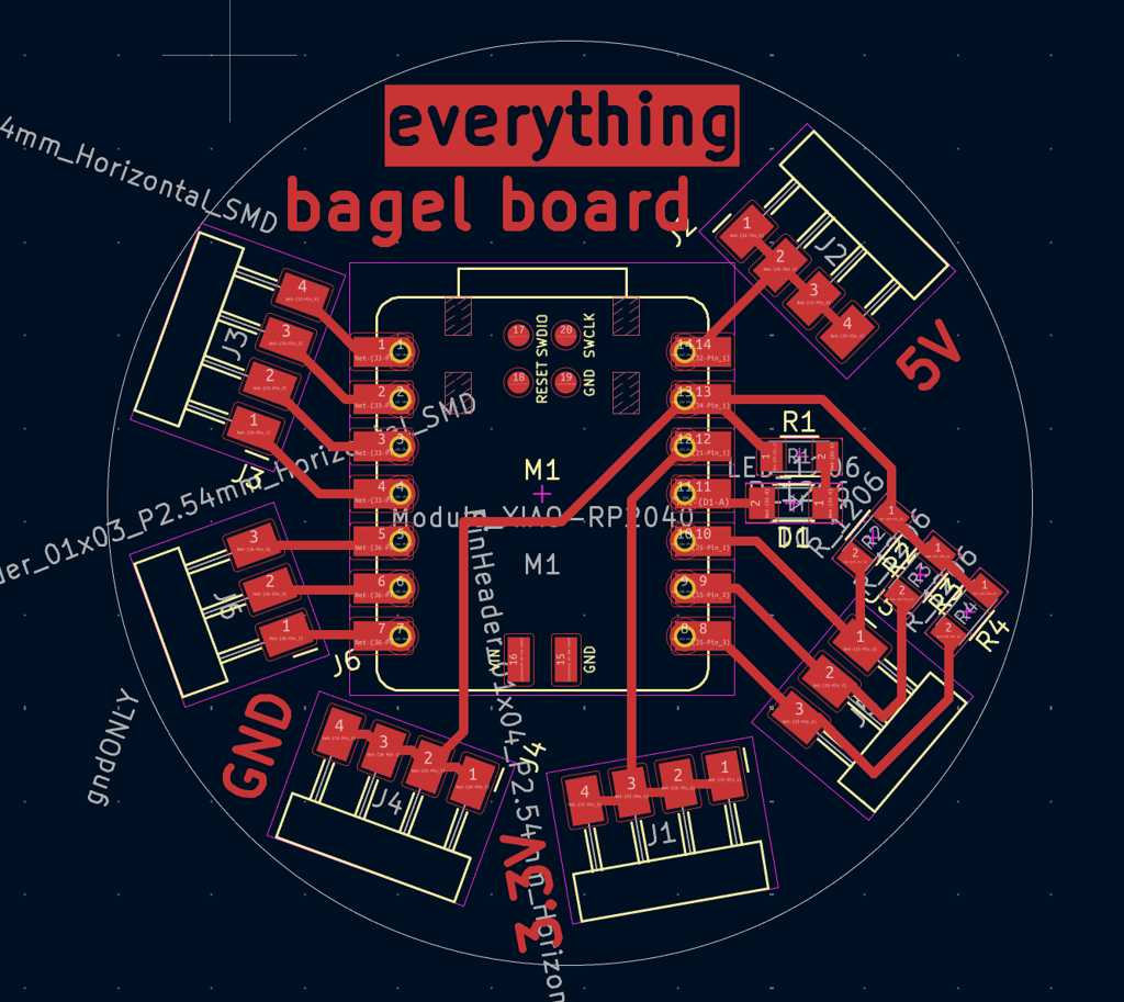
Now that I actually understood how to use KiCad, it was time to create a design that made sense for what I wanted my board to do. For this week's goal, I wanted to make a board that was multi-use and functional—not specialized for just one project. I wanted as many pin headers as possible so I could test and swap wires for different setups. I also wanted to include an LED indicator on the board so I could tell if power was being supplied.
I ended up adding a red LED to my board, along with four-pin headers and three-pin headers. I created the three-pin headers by cutting down a six-pin header—sometimes you have to get scrappy when your lab doesn’t have everything, lol. I added a four-pin header to access pins D0 through D3, and another header for 5V, 3.3V, and ground for easy access. I also added a three-pin header to access pins D7 through D9, and connected a 10kΩ pulldown resistor to that set. For the LED, I used a 220Ω resistor.
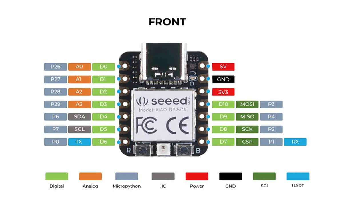
This is the layout I created after thinking through all the components I wanted to include. I referenced the Xiao RP2040 pinout (as mentioned above) to help me decide which pins I wanted to use.
This is my final PCB layout!
Download PCB
Fabricability
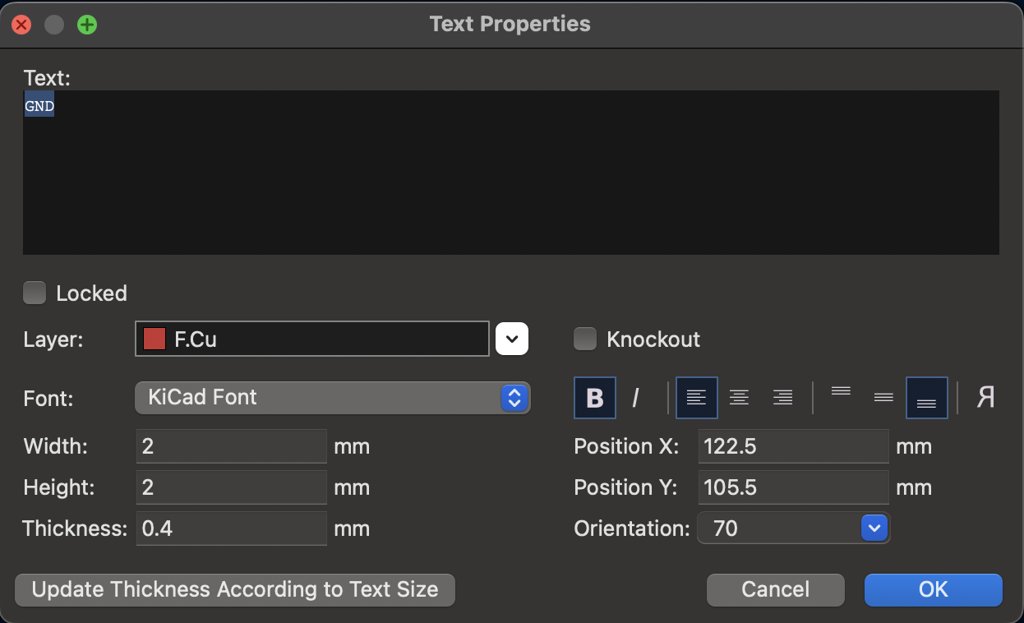
For this week, I didn’t have to actually produce my board, but in order to test the board’s fabricability, I made sure to draw my traces at least 0.4 mm wide. Our class has been having a lot of problems with the mill cutting traces either too thin or too thick, so to play it safe, I bumped mine up to 0.5 mm. I felt that this would protect my board from damage or fabrication issues when I eventually do make it.
The text I chose to include on my board was also adjusted to have a thickness of 0.4 mm or 0.5 mm, depending on how bold I wanted it to appear. I had some trouble figuring this out at first, but eventually realized that to increase the thickness, you also have to increase both the width and height of the text box. I increased the width to 2 mm and the height to 3 mm to achieve the desired text thickness.