Jacob Libby
Week 6
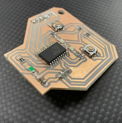
Electronics Design
A week dedicated to designing, fabricating, soldering, and programming a circuit board from scratch
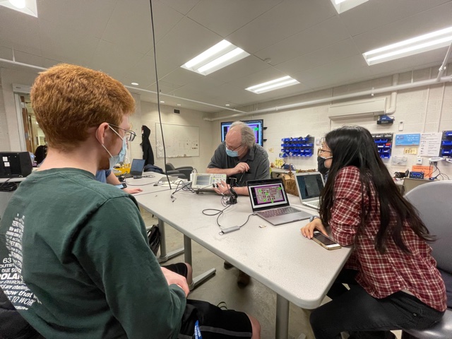
We began this week by in our lab by experimenting with multimeters and a digital oscilloscope. I had taken a course in electronic circuits previously, however this week was incredibly informative and helped solidify knowledge that had definitely grown a layer of dust. We were given a board that was connected to a laptop for power and were asked to test with the multimeter the voltage between the ground and several points on the board. This helped teach us how the electrons flow through the circuit and also showed in a much more tangible way how certain components affect current.
While keeping the black lead on Ground (GND) for the entirety of the exercise, we moved the red lead around the board to test continuity and voltage. We began by testing the voltage at A which was the top right corner of the button and saw that the voltage was 5V, which was equivalent to the input voltage. We then measured the voltage at the top left corner of the button (B) which came out to 0.5mV since the voltage was not currently going through the button. The next measurement was also at the top left corner of the button, but this time we recorded the voltage while the button was being pressed. As we pressed the button, the voltage jumped from 0.5mV up to 5V since pressing the button completes the circuit to the point we were measuring. We then moved across the board to see readings at C, right before the current went through the resistor R2 and got a reading of 5V. Moving the red lead to the start of the LED under R2 (point D), we got the reading of 1.68V, which makes sense since the current travelled through the resistor R2, and thus was reduced when it arrived at point D.
After using the multimeter and getting more comfortable with circuitry, Professor Goodman brought out a fancy digital oscilloscope (I had only used analog ones before) to show us a new perspective. The oscilloscope allows us to see the movement of electrons in real-ish time. This was incredibly interesting to me, but I was through the roof when Professor Goodman pressed the button and explained what was happening.
When the button is pressed on the board, it is programmed to start a ten second timer and print out the time remaining on the computer it is connected to. When the oscilloscope is connected to the board and the button is pressed, we are able to literally see the stream of binary information in 1's and 0's!!!!!!! I am a computer science major, and have always interacted with 1's and 0's in high or medium level programming languages, but I had never actually seen the high and low signals transmit as a current before. This was so cool and definitely one of the highlights of my week!
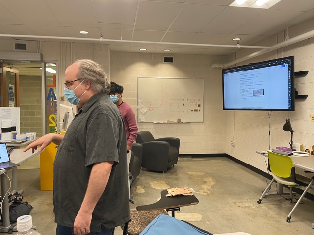
Professor Goodman guided us all through a tour of KiCad, the software that he suggested we learn and use for this week’s project. We went to the GitLab for FabAcademy’s KiCad library and downloaded the file, uploading it into the schematics and footprints of the software. This process took me longer than expected since I had (before meeting) downloaded an outdated version of the FabAcademy library, so I had to do a lot of on-the-fly adjustments and downloading.
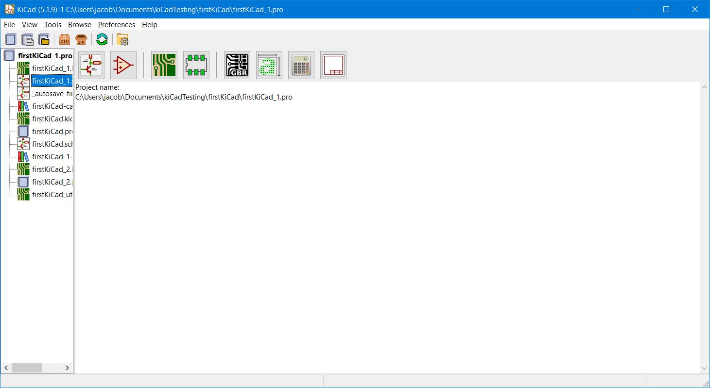
The KiCad software proved to be a little tricky to master at first, especially with such finicky zooming. I decided to plug in a mouse when using this software so that I could use the mouse wheel rather than spending time zooming in and out, and over and over again until I get a better view of my design.
The first view that I used to design my circuit was the Eeschema/schematic view. I was able to add symbols for components into my design and rotate/move them freely. The hardest part of the schematic view for me was remembering the controls and finding the correct components. However, I really enjoyed the task of connecting the components with wires, and it brought back fond memories of me using Logisim, a similar tool used to create logical gates and circuits.
My hope for this design was to create a board that had two buttons and three LEDs to create a simple coordination game. My plan is to code this board to have each player press one button each at the same time. If the buttons were pressed in a number of milliseconds within eachother, the green LED would light up. If one person pressed their button after the other with a delay longer than that, the LED closest to their button.
The next step of the process was to create the tool paths for the traces on the copper surface. To accomplish this, I used the PCB view, and began connecting components with 0.5mm copper trails. This process was surprisingly fun. It was like a complex puzzle (and reminded me of the mobile app/game: Flow Free) that kept me thinking even while I was away from my computer. I created the design above while trying to optimize the size of the design, and thus had to redesign. Although this design had a very small footprint, I was hoping to create a circuit that was symmetrical in its button and LED placement, and found later I did not include two pull-down resistors.
My next iteration took far more time to put together, as there were now more components and thus far more constraints on the design. After tedious randitions of getting to the lasts components and it being impossible to connect then with a trail of copper that wouldn't create a short circuit, I rejoiced when I created the above design. Although reminiscent of a concerned skeleton, I am extremely proud of this design and am incredibly happy with how it turned out.
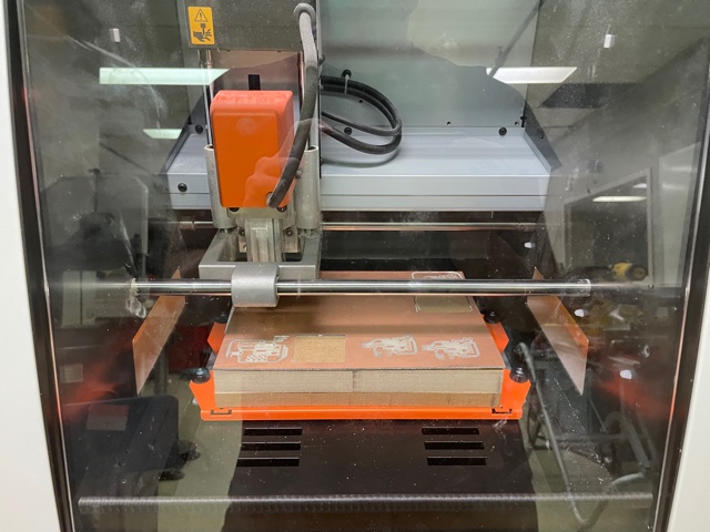
The next step was to fabricate the design with the roland mill. I uploaded the design as an SVG to illustrator, double checked the nodes and connections to see if there were any errors/issues, re-traced some copper paths, reuploaded to illustrator, and sent the file into Mods.
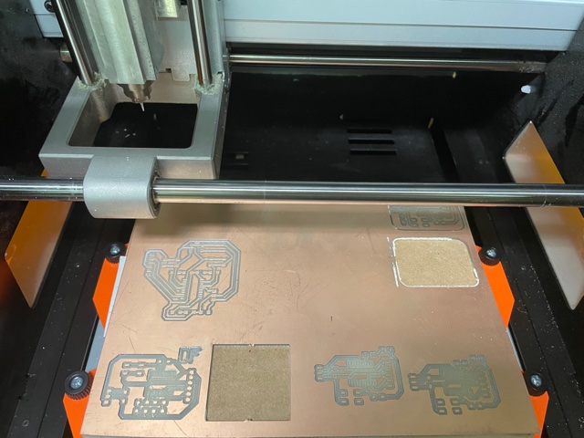
After zeroing the mill and performing a series of air cuts, I first cut the trace of the design. During this cut, it was evident that I did not correctly zero the mill as it was barely scraping the top of the copper, and thus had to abort the cut, re-zero the mill, and then start the cut again. This cut went much better.
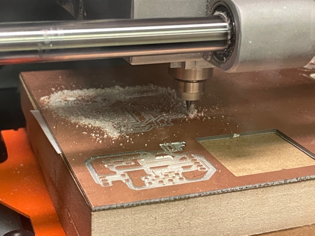
I then changed out my bit to a 1/32" carbide end mill and repeated the same steps. I went to illustrator, double checked the design, uploaded to mods, performed an obsessive amount of air-cuts, and then mustered the guts to cut into the material. I first cut out the holes for the connectors and keychain hole, and then the outside cut.
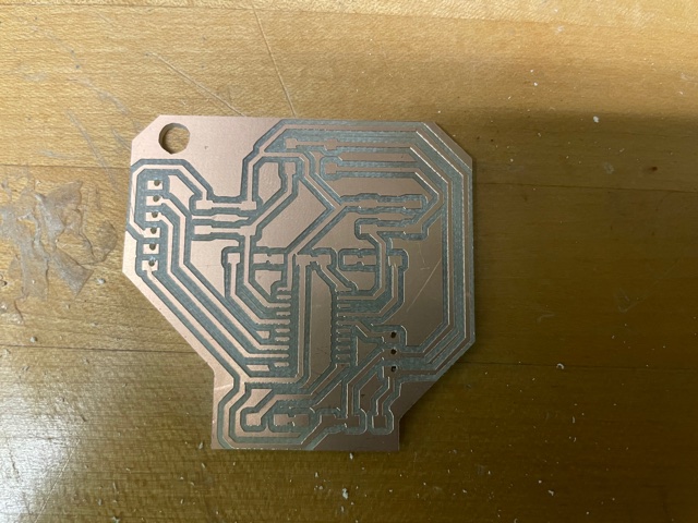
These came out beautifully. I then went to sleep in order to not be as shaky for soldering the next day. After week 4, I felt much more confident in my ability to create a circuit board and (in comparison) flew through the soldering process. I was using a heatgun for all solders except for the pins, for which I used a solder iron. The hardest part of the soldering process was keeping my hands steady and soldering the areas of the design that had copper going under components. I had to make use of Neil's strategy of "heating up a component while holding onto it with tweezers until the board came loose and fell" a few times since I was getting more connections in areas than I was planning. In addition, an area of my board (above pin 1 of the ATiny1616) was connected by copper in a way that it should not have been. I tested this area with a multimeter and it had continuity with less-than desirable parts of the board, so I had to chip away at the extra copper that was creating the bridge, and after testing the continuity again, found I had fixed the problem and probably saved me a lot of time if I had plugged it in and something short circuited or blew up.

After I had finished soldering and had tested my board with a multimeter a few more times, I moved on to programming the board.
I downloaded Arduino and got to work with connecting my board to my computer. I copied over Neil's Echo Hello code and after changing the code from 1614 to 1616-compatible, I clicked "upload using programmer" to upload the code onto the board. After this, and a bit more trouble shooting and switching the Tools->Chip to the correct 1616 chip, I then reconnected my board with the FTDI pins in order to have the board and the computer communicate with eachother. The next crucial step was to cross my fingers. After quadruple checking the connections to make sure I had connected all pins correctly, I tried over and over again by opening the serial monitor to create communication between the board and the computer. After asking for help from fellow classmates, we realised a common problem among our boards and found that by adding a line "Serial.swap();" under the void setup() funciton, this allowed the communication to occur and fixed the code.
I crossed my fingers again and was thrilled when my board said "hello" back!!!!! It worked! I felt so accomplished.
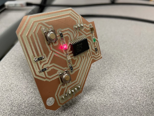
This week was an incredibly challenging week, and I am extremely proud of what I have accomplished. The process of going from design to fabrication to electronics is tedious, long, and full of hurdles, but it is also so rewarding.
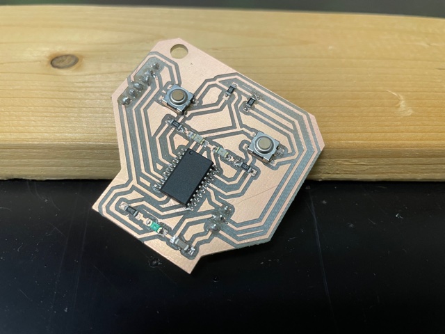
I look forward to working again with electronics later on in this course and completing the program for this board.