Mohit Ahuja's Fabacademy 2021
Output Devices
Group Assignment
This week did some measurements of the power consumption by different boards. This is the result of the group project:
Link to the group assignment page
Individual Assignment
Out of all the weeks so far, I have definitely done the most work in Output Week. This week I really went on a full on spree of making interesting things, and I got so lost into it that my documentation suffered because of it. But not to worry, I will take you through the entire journey of my exploration of making an output device.
After a lot of pondering, I chose an OLED display for my output device, because I wanted to incorporate OLEDs into my Final project too. Hence this week was the perfect time to get my feet wet with using the OLED display. I went through a total of 3 complete redesigns of my board, and I am still a little bit unhappy with the result. But let us move through the process to see what I did, what issues I faced, how I made it work eventually and what do I need to improve.
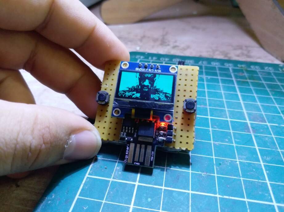
I had actually already made the previous version of the Charlieplexing circuit back in 2017, so there was an option to do that yet again, maybe with a twist. But I realised that for the kind of data that I want to display, an OLED would be a much better alternative. And I already had an idea that this was going to work, mainly because I had already made a project that involved connecting a Digispark ATTiny85 module to an OLED along with 2 buttons that would input some kind of data to the microcontroller. My intention for making that was to make a configurable digital watch, and maybe even a smartwatch some day. Here are a few pictures of the prototype featuring the late Chadwick Boseman as Black Panther:
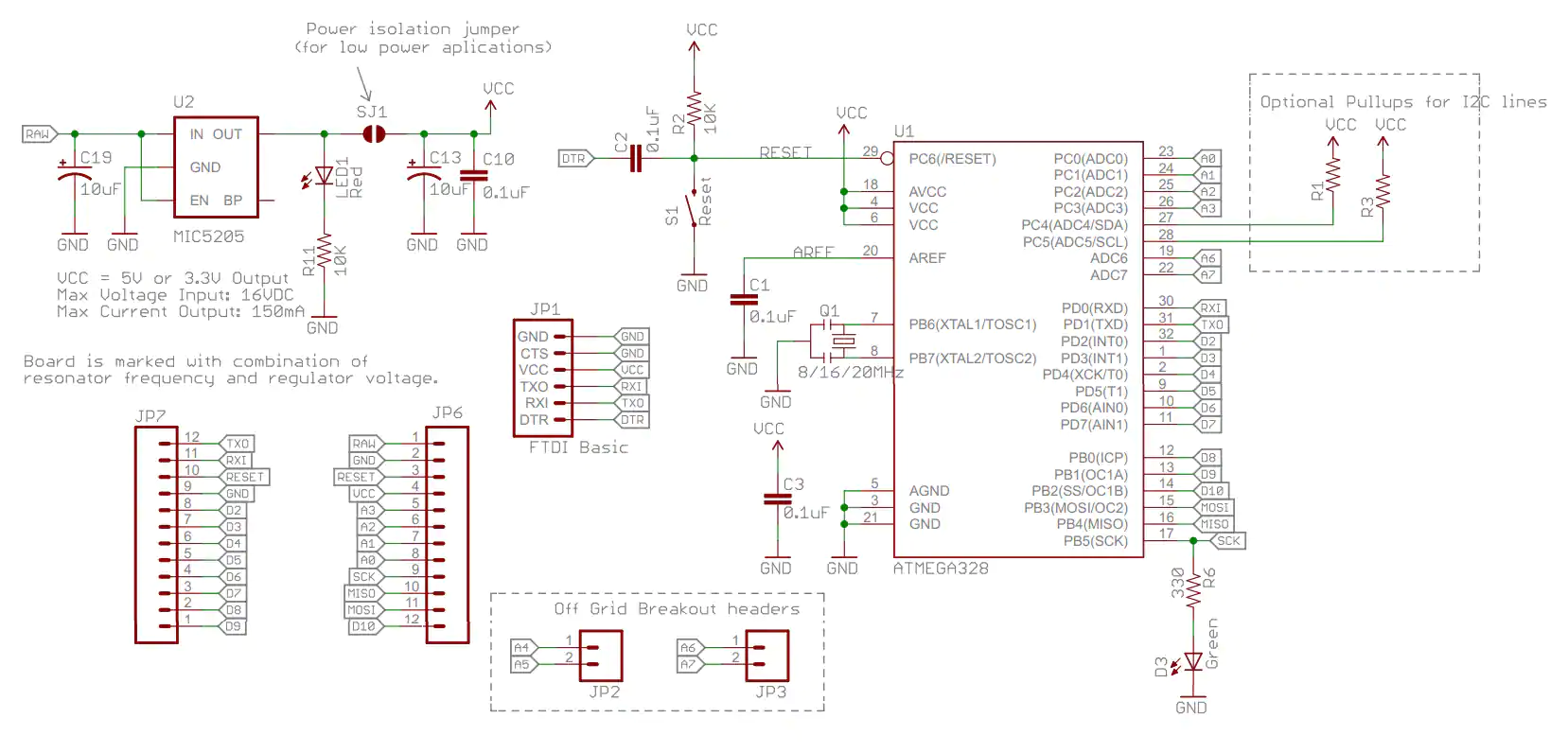
I talked about this with Suhas Sir, who told me that he had tried making the OLED board in the past, but hadn't found success since the attiny45 had very little memory space. To which I agreed, because when I had made the code for the perfboard version of the circuit, I had used up almost all of the memory space. So he pushed me to try to make the OLED board, if not with an attiny45 then with an attiny85. He actually suggested going for the atmega328 chip first, since it would be easier to interface and would have no limitations regarding memory. I was reluctant about that since the atmega328 would be very wasteful for a project like this, because it would have too much memory, and too many unused pins.
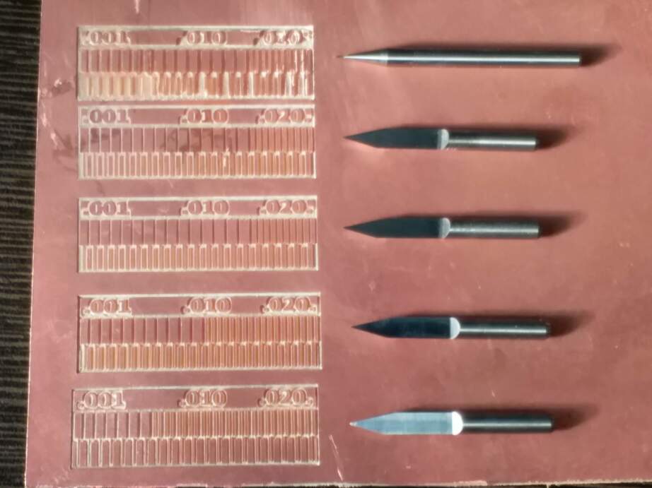
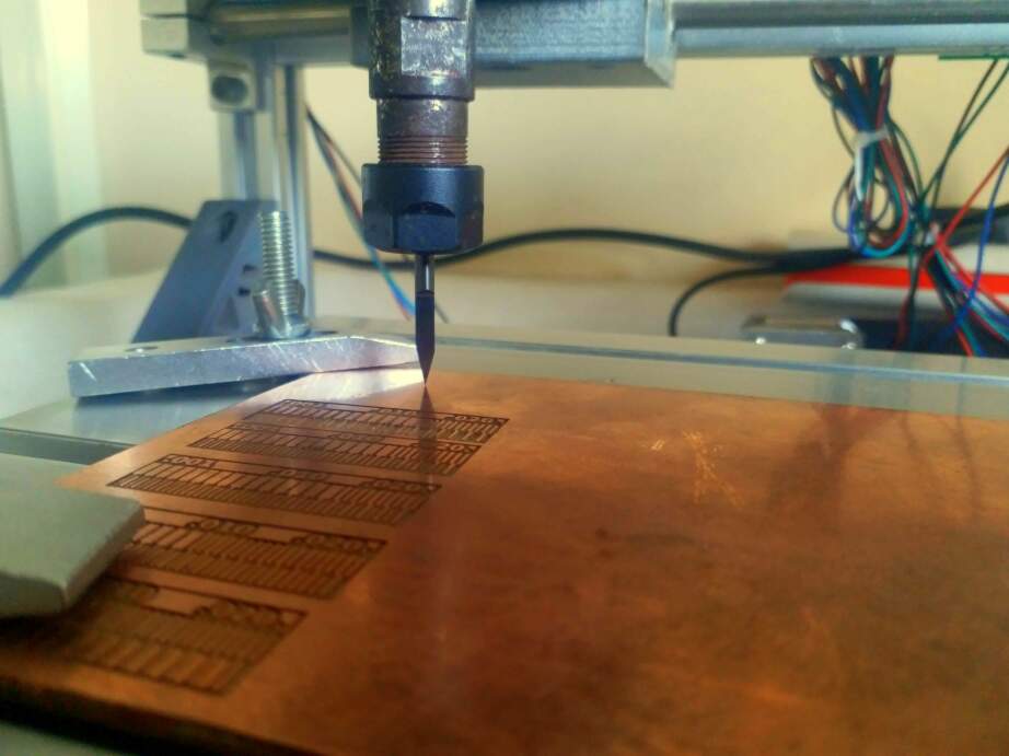
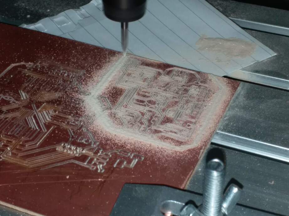
Caliberating the PCB Milling machine
First Iteration
For making the first version of my board, I took Suhas Sir's suggestion and went ahead with the atmega328 for my board. I also wanted to make the circuit rechargeable and also wanted to have a boost converter that converts the 3.7V-4.2V of the Battery to 5V.
So I looked up the components that were used to make a TP4056 Li-ion/Po Battery charging module and found this schematic:
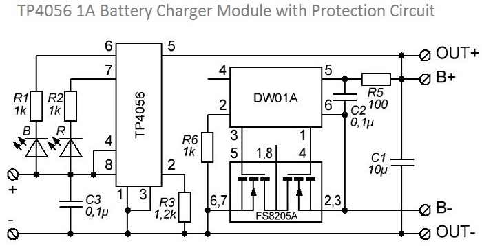
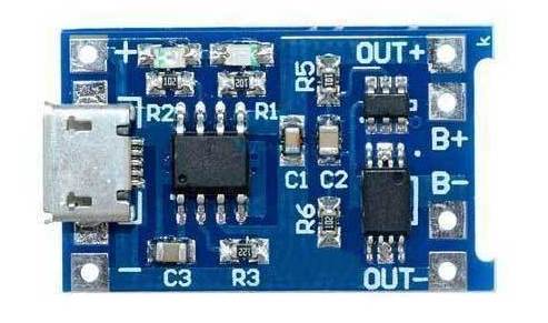
This page explains the circuit very well. I also recommend going through this page for some extra info on how to charge multiple batteries from a single.
I'll try to summarise everything I have read so far about this module. Essentially the TP4056 module consists of 3 primary components: Ø TP4056 IC: The TP4056 is a complete constant-current/constant-voltage linear charger for single cell lithium-ion batteries. Its SOP package and low external component count make the TP4056 ideally suited for portable applications. Furthermore, the TP4056 can work with USB and wall adapters.
- TP4056 features include current monitor, under voltage lockout, automatic recharge and two status pin to indicate charge termination and the presence of an input voltage. This IC is responsible for charging and protecting the Li-ion battery. Here is a link to the datasheet for the IC with all the characteristics, and a recommended circuit too.
- DW01A: The DW01A battery protection IC is designed to protect lithium-ion/polymer battery from damage or degrading the lifetime due to overcharge, overdischarge, and/or overcurrent for one-cell lithium-ion/polymer battery powered systems, such as cellular phones. Here is a datasheet of the IC which also shows a recommended circuit for using the IC.
- FS8205A: This Dual N-Channel Enhancement Mode Power MOSFET is used for cutting off the battery voltage when the battery is drained below the safe limit. Here is the datasheet of the IC containing all the relevant info about how to drive the IC.
But the voltage output of this would be between 3.0V - 4.2V, and the atmega328 needs a constant 5V regulated source of voltage for operation.
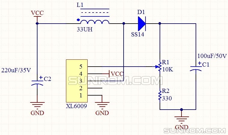
So I decided to add a boost converter to my project too. I decided to put the components of an existing boost converter module that is commercially available. The boost converter I chose was based on the XL6009 IC, and here is the schematic of the module:
This was the schematic of the first version of the board:

And this is the board design:

Click on the images below to download full resolution png images of the traces and cutout files:


Second Iteration
This is the second version of my board, I removed the ISP from the board.
This was the schematic from the second board:
This is the board design:
Second Iteration Schematic
Second Iteration Board
Click on the images below to download full resolution png images of the traces and cutout files:

This is the milling result:

Third Iteration
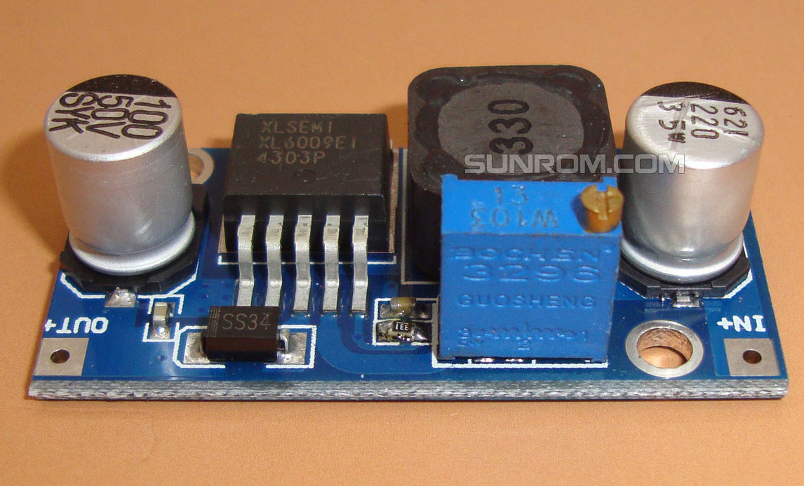
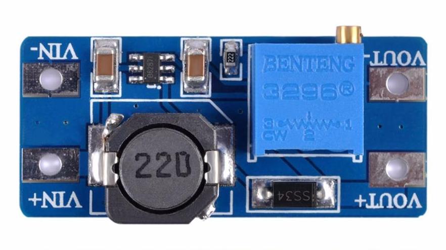
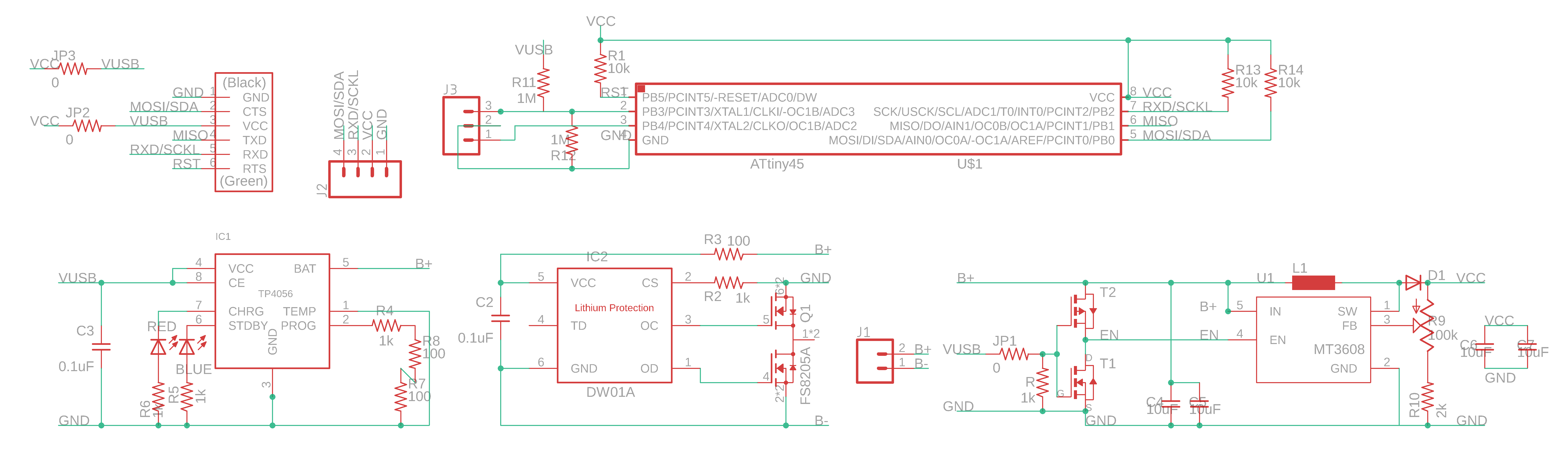
This is the third version of my board, I changed the boost converter to an MT3608 that I extracted from this commercially available boost converter module:
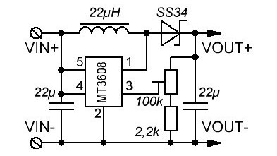
This was the schematic from the third board:
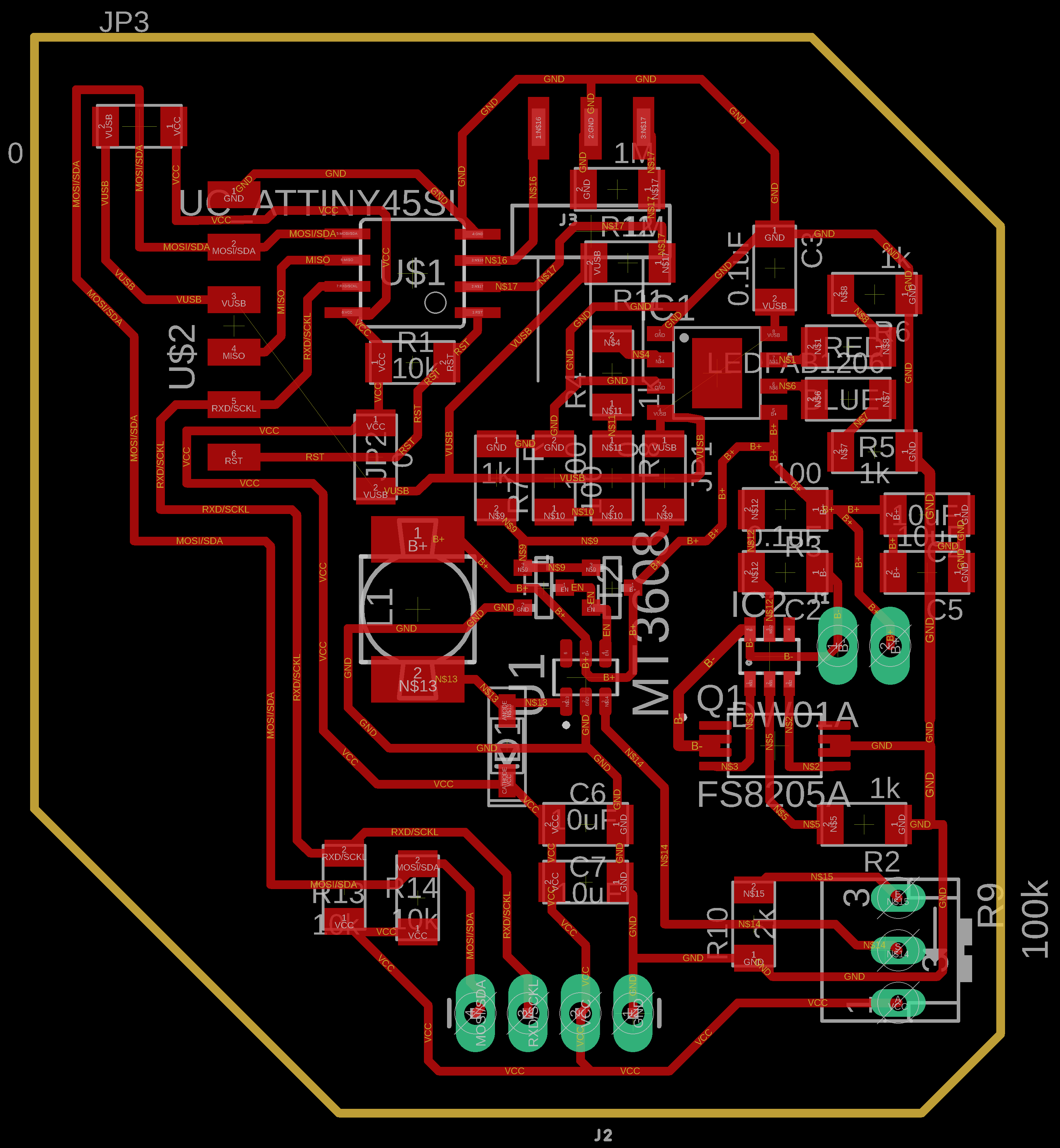
This was the board design:
Click on the images below to download full resolution png images of the traces and cutout files:

This is the milling settings:


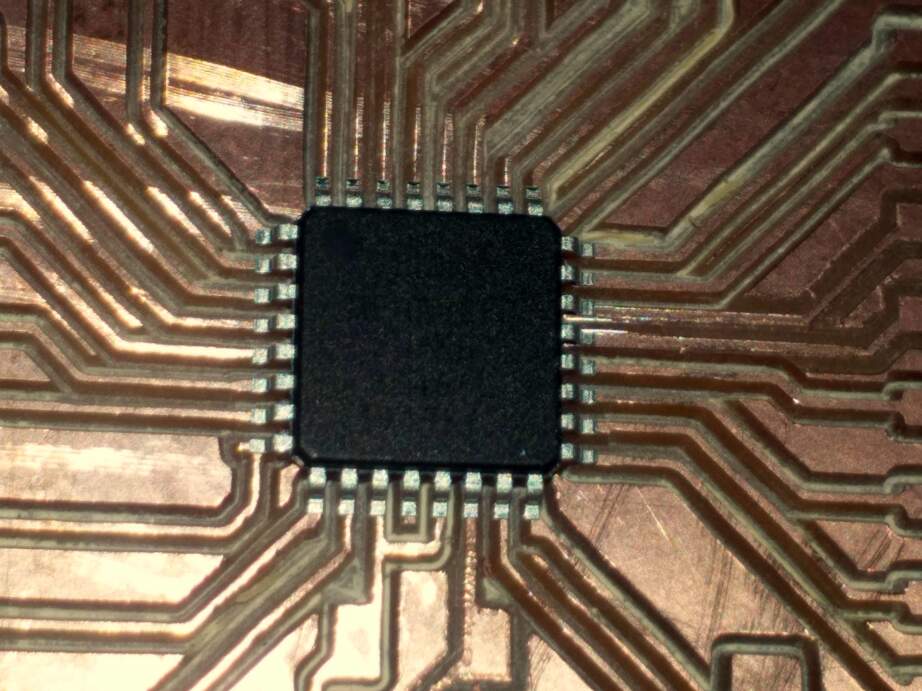
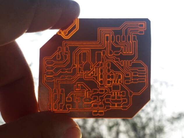
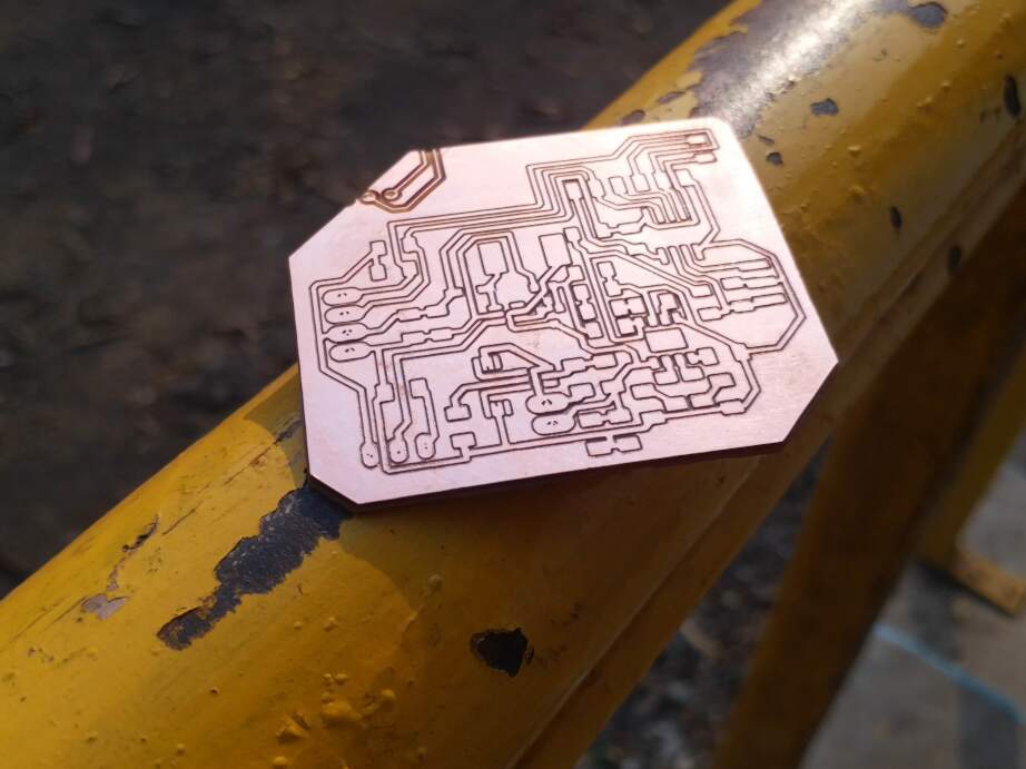
This was the outcome of the milling process:
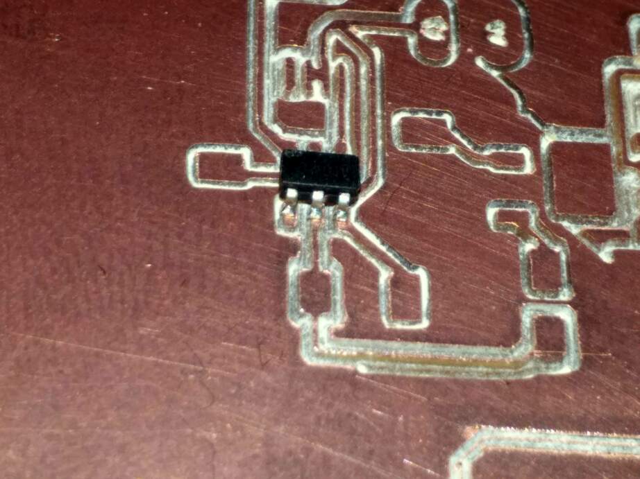
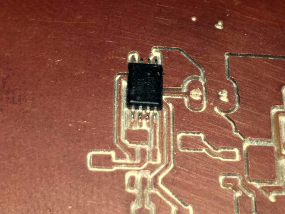
After soldering and stuffing, this is the result:
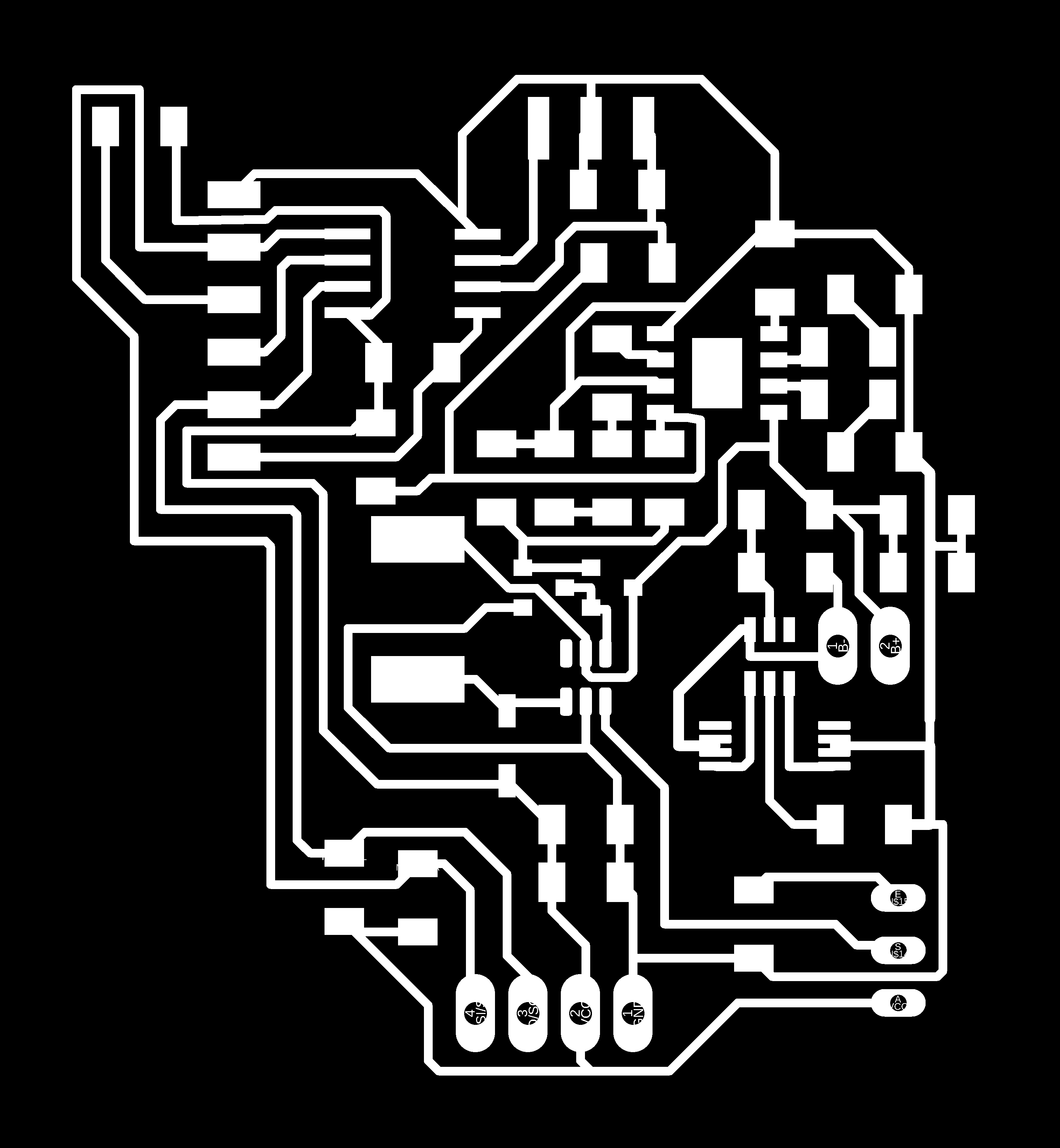
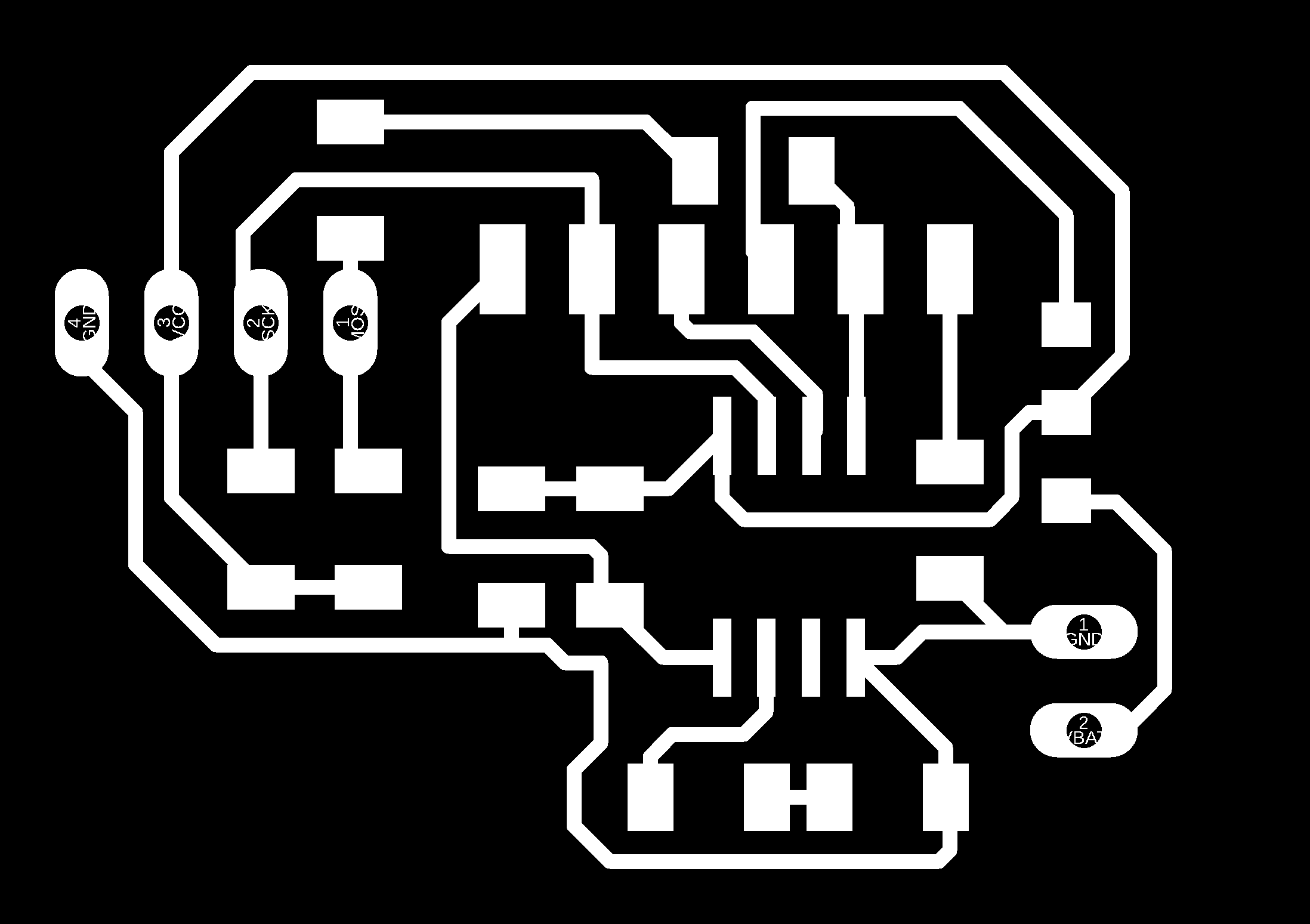
Fourth Iteration
For this iteration, i decided to make the board without any bells and whistles whatsoever. I decided to get rid of the battery charging and boost converting circuits and make a simple driver board. This was the schematic and the board design:
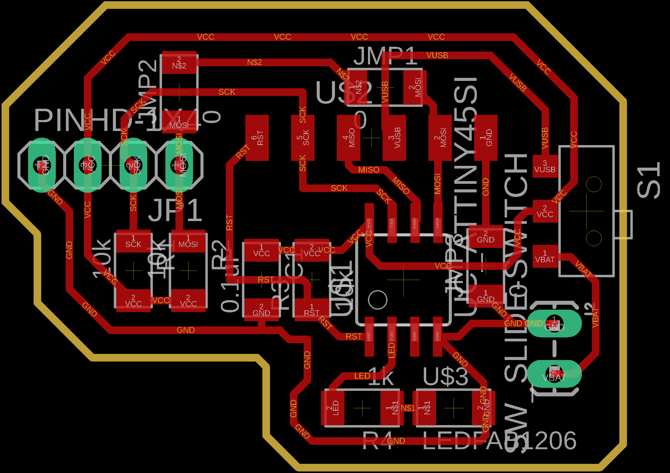
Fourth Iteration Schematic
Fourth Iteration Board
Click on the images below to download full resolution png images of the traces and cutout files:

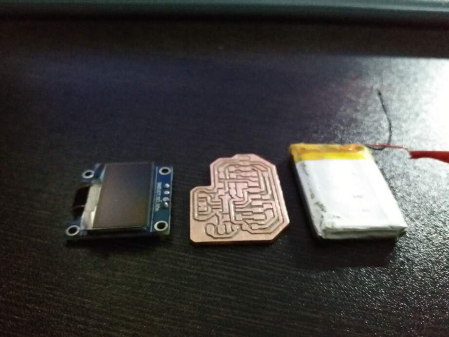
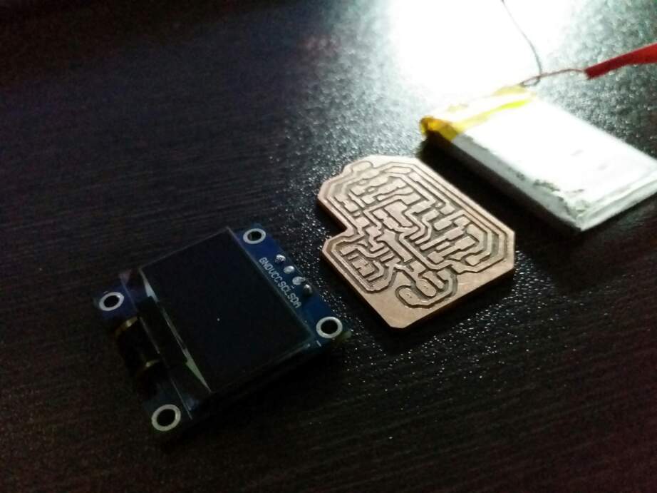
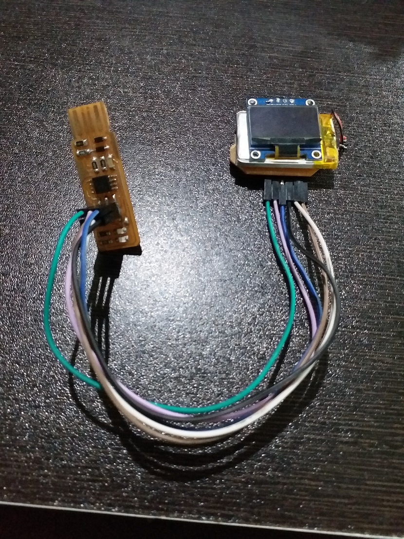
And here is what the finished board looks like:
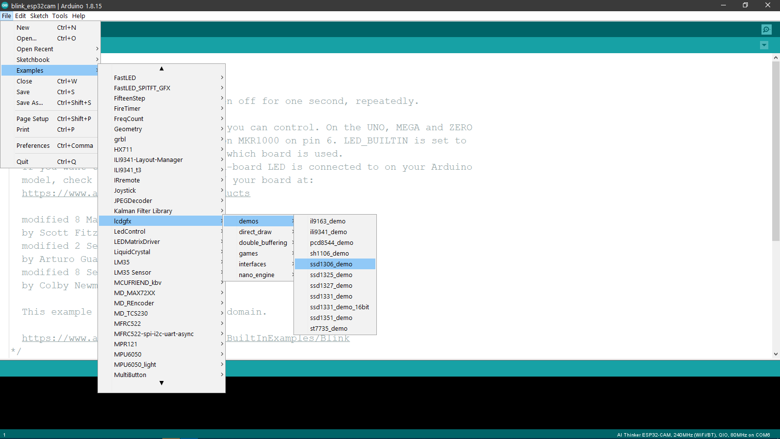
To program the board, I used the example from the lcdgfx library by going to File>Examples>lcdgfx>demos>ssd1306_demo
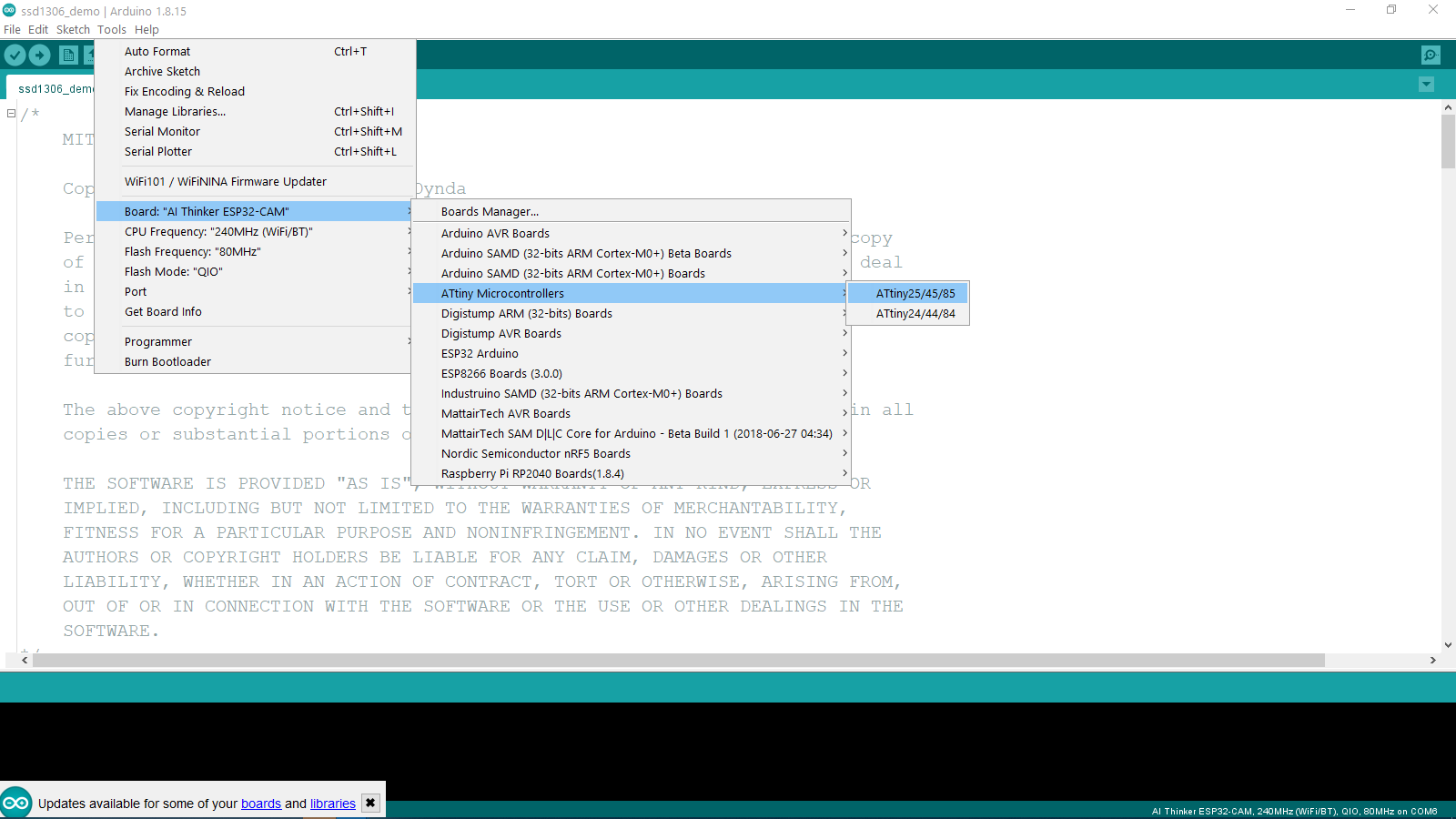
To upload the code to the board, I selected the correct board from Tools>Board>ATTiny Microcontrollers>ATTiny25/45/85
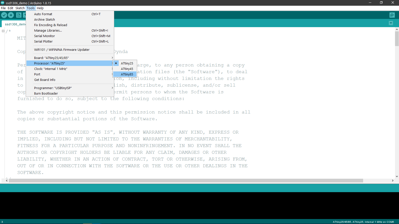
Then I selected the correct microcontroller from the newly created menu under Tools>Processor>ATtiny85
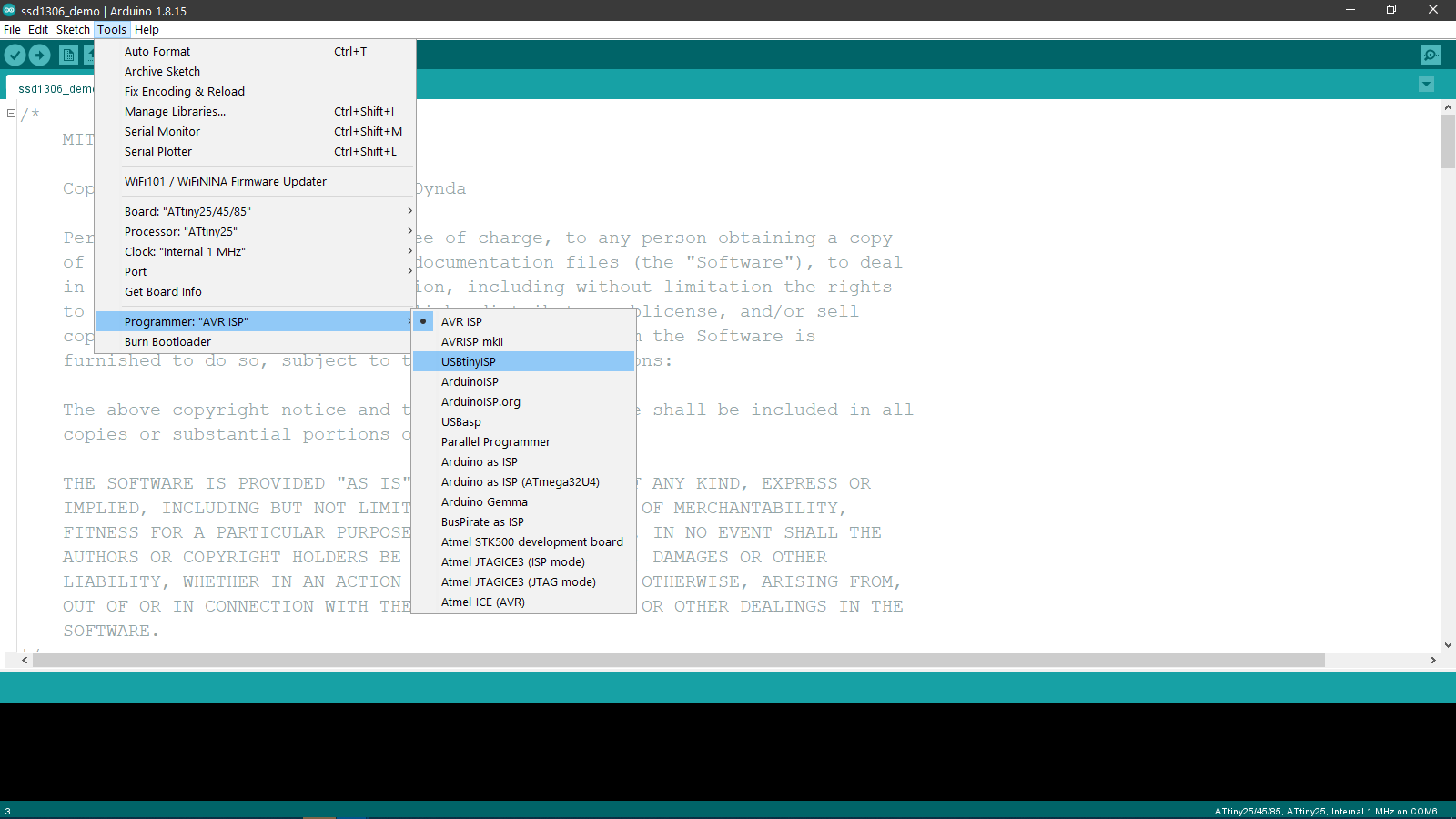
Finally I chose the correct programmer for my FabISP from Tools>Programmer>USBtinyISP
This is the LCD demo code for the board
These are the connections I made to the board with my FabISP to program it:
After uploading the code for the firs time, I noticed that the LCD was not working. When I read the comments before the program that I uploaded, I realised that the connections for SDA and SCL suggested by the program are different from the default SDA and SCL pins of the attiny85 ic.
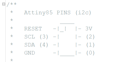
The pinout suggested by the code
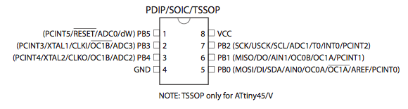
The pinout of the IC by default
This was why the code did not work properly when I tried it for the first time. I tried to see if I could change the pins within the program to the original pins of the attiny85, but I realised that it would be very difficult for the limited time I had. So I had to make some changes to the connections. I simply took the SCL and SDA pins of the LCD and directly soldered them onto the suggested connections by the program.
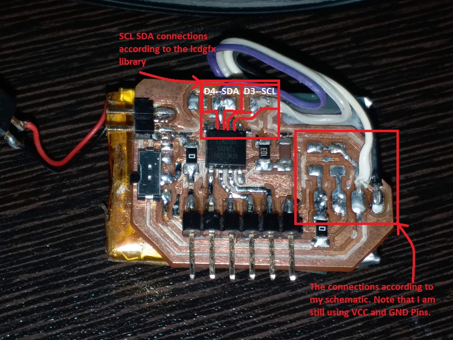
It is not the prettiest, but it fixed the issue and the LCD started to work. In the future I will fix the schematic and board files and make a better version of the same.
Finally, this is the result of the entire ordeal:

Power Consumption of the board:
The above video shows a multimeter measuring the current flowing through the circuit. You can see that the current consumption changes based on the number of pixels that are lit on the display. Based on this video, we can discern that the average power consumed by the circuit at a voltage of 3.7V (typical lithium polymer cell voltage) like so:
- Average current consumed by the circuit: 13.72mA
- Typical Voltage of a Li-Po Cell: 3.7V
- Therefore, Power = Voltage * Current = 3.7 V * 0.0137 A = 0.051 W = 50.764 mW
The project consumes 50.76 mW of power with the program that it is running currently.