The assignment for this week was to learn the basics of electronics production by milling PCB board with a benchtop CNC machine, and soldering the components to it. This week there were group and individual assignments. The assignments were:
Group assignment
- Characterize the design rules for your PCB production process: document feeds, speeds, plunge rate, depth of cut (traces and outline) and tooling.
- document your work (in a group or individually)
Individual assignment
- Make an in-circuit programmer by milling and stuffing the PCB, test it, then optionally try other PCB fabrication process.
The learning outcomes were to:
- Describe the process of milling, stuffing, de-bugging and programming
- Demonstrate correct workflows and identify areas for improvement if required
To discuss the work completed this week I will share first the group assignment, and then the individual assignment.
Group Assignment
The objective of the group assignment was to Characterize the design rules for our PCB production process: document feeds, speeds, plunge rate, depth of cut (traces and outline) and tooling, and document our work (in a group or individually). To begin, I will start with describing the hardware.
CNC hardware
The CNC milling machine that we used was the Carvey tabletop 3D carving machine as shown in the image below.

The technical specifications are as follows:
- Machine Footprint: 24" x 24" x 18” (61cm x 61cm x 46cm)
- Work Area: 12” x 8” x 2.75” (30cm x 20cm x 7cm)
- *Repeatability 0.001" to 0.003"
- Run out: .0006" (.01524mm)
- Spindle RPM: 3000-12,000 (300W)
- Weight Approx: 60 lbs. (27kg)
- Materials it Can Cut: wood, soft metals, foam, plastics, circuit boards
- Connectivity: USB Port
- Computer System Requirements: Chrome web browser, 64 bit Mac or Windows, USB Port.
the first part of the group assignment was to learn how to use the machine, this included loading the cutting piece, working with the software, changing the bit, and starting a carve. The Vancouver Fab instructor Jason provided the instruction and we made the video below as reference.
Characterising the machine
After we had learned how to operate the CNC machine, the next step was to begin characterising the various aspects of its performance. To do this we performed three different tests:
- a line test: to characterise the precision (trace) of the bit
- speed tests: to characterise the speeds and plungerates
- depth tests: to characterise the depth setting needed to penetrate the copper.
All of the characterisation was done with a 30 degree V-bit as shown in the photo below:

The first test we performed was the line test. In this test, we milled various lines to see how precise the bit could be. For these tests we used the following settings:
- Bit size: 0.1 mm
- Cut depth: 0.01 in
- Feed Rate: 9 in/min
- Plunge Rate: 6 in/min
- Depth per pass: 0.005 in
The result of the cut test was as shown in the photo below:

The next major tests that were carried out, were the speed tests. In these tests we varied the speed and plunge rate to see what the maximum we could do was without damaging the bit. We tried the following different settings.
- Bit size: 0.1 mm
- Cut depth: 0.01 in
- Feed Rate: 15 in/min
- Plunge Rate: 10 in/min
- Depth per pass: 0.005 in
- Bit size: 0.1 mm
- Cut depth: 0.01 in
- Feed Rate: 20 in/min
- Plunge Rate: 12 in/min
- Depth per pass: 0.005 in
- Bit size: 0.1 mm
- Cut depth: 0.01 in
- Feed Rate: 5 in/min
- Plunge Rate: 6 in/min
- Depth per pass: 0.005 in
In two of these tests we broke our bits. Therefore we settled on the following settings as ideal for our setup:
IDEAL SPEED SETTINGS
- Feed Rate: 7 in/min
- Plunge Rate: 6 in/min
The final, and most critical tests we carried out were the depth tests. After several tests, we made the observation the the zero sensor was not calibrated correctly, so we adjust its height and proceeded to test at various depth settings. For brevity, I will list the settings of all the tests on one line.
Bit size: 0.1 mm Feed Rate: 7 in/min Plunge Rate: 6 in/min Cut depth: 0.0001 in, 0.0002 in, 0.0003 in, 0.0004 in, 0.0005 in Depth per pass: 0.0005 in
The results are shown below:

Bit size: 0.1 mm Feed Rate: 7 in/min Plunge Rate: 6 in/min Cut depth: 0.0037 in, 0.004 in, 0.005 in, 0.006 in, 0.0065 in Depth per pass: 0.0037 in, 0.004 in, 0.005 in, 0.006 in, 0.0065 in
in these test we found that a value of depth below 0.0037 in DID NOT CARVE the material. This was a result of the miscalibration. Therefore we learned that we had to add 0.0037 in to our desired cut depth to get the desired cut. We also learned that the copper is not penetrated until a depth setting of about 0.0051 in. The results for this test are shown below.

Through the this testing we determined the ideal settings as follows:
IDEAL SETTINGS FOR PCB V-BIT
- Bit type: V-bit
- Bit size: Select 0.3 mm
- Feed Rate: 7 in/min
- Plunge Rate: 6 in/min
- Cut depth: 0.0052 in
- Depth per pass: 0.0052 in
IDEAL SETTING FOR PCB END-MILL
- Bit type: end-mill
- Bit size: 0.18 mm
- Feed Rate: 20 in/min
- Plunge Rate: 10 in/min
- Cut depth: 0.004 in
- Depth per pass: 0.004 in
Individual Assignment
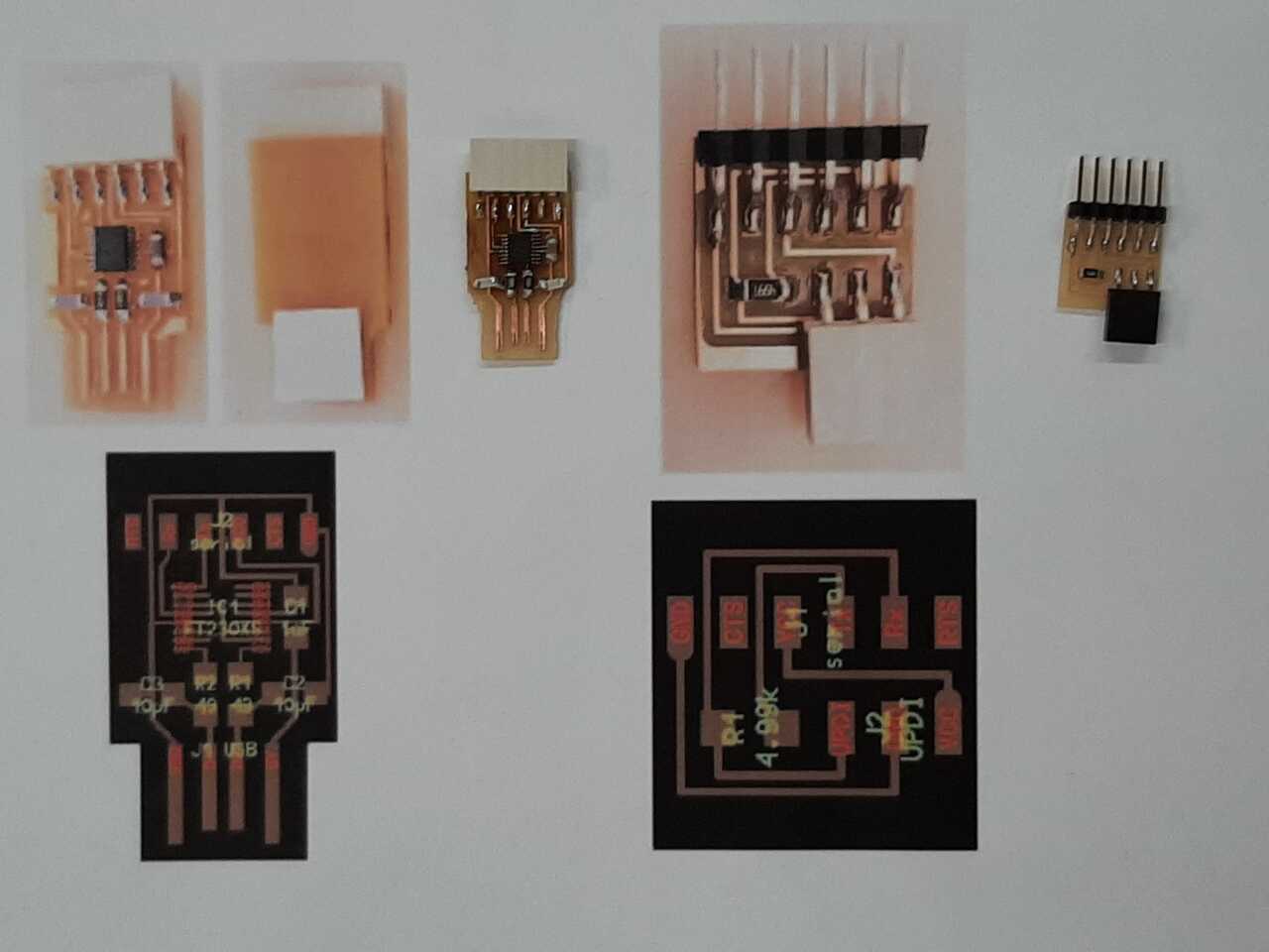
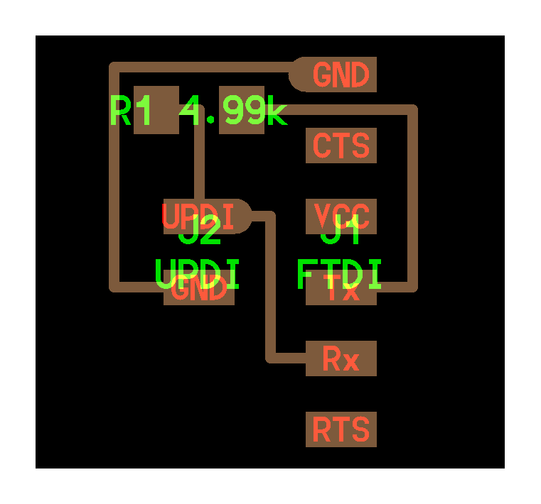
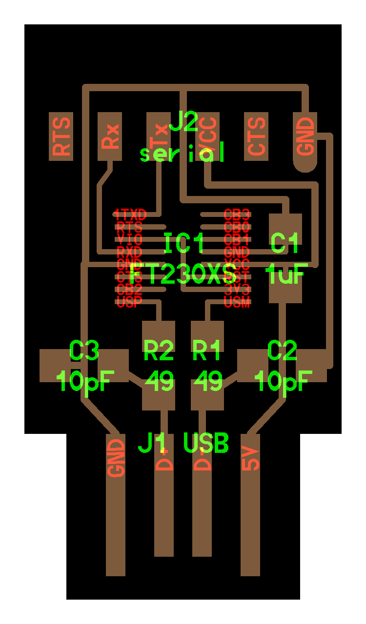
Following the characterisatoin efforts performed as a group, and satisfied with the settings we had established, I then began to work on my individual assignment of creating a UPDI circuit board and an FTDI circuit board in order to make a UPDI to FTDI adapter. I began by cutting the UPDI board first with the following result.
Millinh
I used the following settings for milling my UPDI and FTDI boards
Bit size: 00.1 mm Plunge Rate: 6 in/min Cut depth: 0.0052 in Depth per pass: 0.0052 in


I then began attempting to cut the FTDI chip out of the PCB board using the following settings:
Bit size: 0.1 mm Plunge Rate: 6 in/min Cut depth: 0.0052 in Depth per pass: 0.0052 in
and achieved a rather disappointing result.

the issue was that some of the traces would get cut away by the bit. After some hypothesizing, it became apparent that there were two issues at play
-
- The tip of the bit is 0.1 mm, but at the surface level it is wider because it is a v-bit
-
- When the software is set at 0.1 mm it will program more passes, thus resulting in more material being cut
So I went about trying to resolve this issue through further characterisation. The first step was to do some simple geometric calculations to determine whether the width of the bit at the top of the surface was substantially greater than at the cutting depth (tip of the the bit). The image below illustrates the calculation performed:

The result was 0.135 mm, a difference of 35%, therefore it was not trivial. The other consideration was the effect on the bit size setting on the number of passes programmed by the computer so I went about playing with the bitsize width (as per the image above) until I converged on the ideal bitsize setting.
IDEAL PCB CUT SETTINGS
- Bit size: 0.35 mm
- Feed Rate: 7 in/min
- Plunge Rate: 6 in/min
- Cut depth: 0.0052 in
- Depth per pass: 0.0052 in
with these setting I was able to obtain the following result:

The next step was to stuff the UPDI and FTDI boards. The components required for each board are listed as follows:
UPDI board
- 3 pins female header
- 6 pins male header
- 4.99 k resistor
FTDI board
- 6 pins female header
- 2 x 49.99 ohm resistor
- 2 x 10 pF capacitor
- 1 uF caoacitor
- FT230XS (missing)

The image below shows the final soldered UPDI board.

Soldering
The next step in the process was to stuff the board by soldering the chip into place. The first step is to solder the microchip onto place. this can be done with a soldering iron or a heat gun. Flux is extremely helpful in doing this as well.
First we start with all of the parts

Next we solder the chip into place


After we solder the other components such as resistors and capacitors.

lastly, you will want to test that all of the connections are properly soldered by using a continuity test on the multimeter. A photo of this process is shown below.

If all is well it is time to move ahead to programming and debugging. Below a photo of the two soldered boards.

Programming/debugging
The first step in the process is to download and ensure that you have installed the FTDI driver onto your computer so that it will recognize it as a USB device. You can do this by going to ftdichip.com/drivers/vcp-drivers and downloading the driver for your OS.

Once downloaded you can extract the folder to your desktop or other prefered folder location on your computer.

Now plugin and connect your FTDI board into your USB port. Note that the use of a cable helps to relieve pressure on your computer board and your fabricated board.

Lastly, you will want to go to your device manager and ensure that your FTDI chip is being recognized as a COM/PORT

and voila, you have your FTDI chip to program your boards. Connect this with the UPDI board to program AT-Tiny chips
