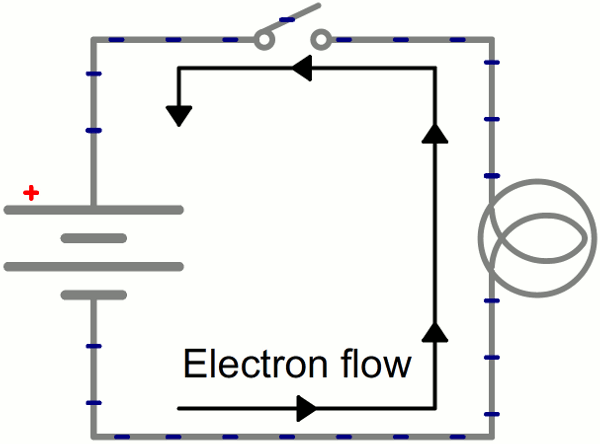
A vital point before start drawing or even designing PCB is to explore both; the workflow of a circuit and the current. This tutorial includes the explanation of the circuit and how it works. While, this tutorialexplores the workflow of the voltage and current.
GOAL
Redraw the Eco Hello world board that has Microcontroller attiny45 board through using different Microcontroller (i.e; attiny44 or atmega328) and including at least one LED (with current limiting resistor) and one button.
EXTRA CREDIT:Add different inputs and outputs.
LEARNING OUTCOMES
Select and use Autodesk Eagle software to design a printed circuit board (PCB).
Demonstrate workflows used in designing a printed circuit board and that’s through designing the circuit schematic to be then converted into an electronic board.
SOFTWARE USED TO BUILD PCB
Autodesk Eagle.
WORKFLOW TO DESIGN A PCB
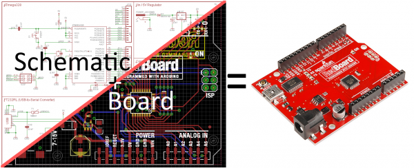
Schematic phase: schematic diagram encompasses of components and wires that connected with the purpose of producing the electrical circuit. On other word, the schematic diagram illustrates how every different component of a circuit is connected to each other. In addition, the diagram shows how lines represent connecting wires otherwise the basics such as; resistors, lamps, and switches which are represented by consistent symbols, thus making the board’s routing easier.
Layout phase.
Milling phase.
Soldering phase.
DEFINITION OF PRINTED CIRCUIT BOARD
Printed Circuit Board also known as "Printed Wiring Boards" or "Printed Wiring Cards". PCB is a flat, rigid, and insulating material which includes a conductive structure that adhere to one side. The conductive structures create a geometric pattern which contains; rectangles, circles, and squares (as an example).
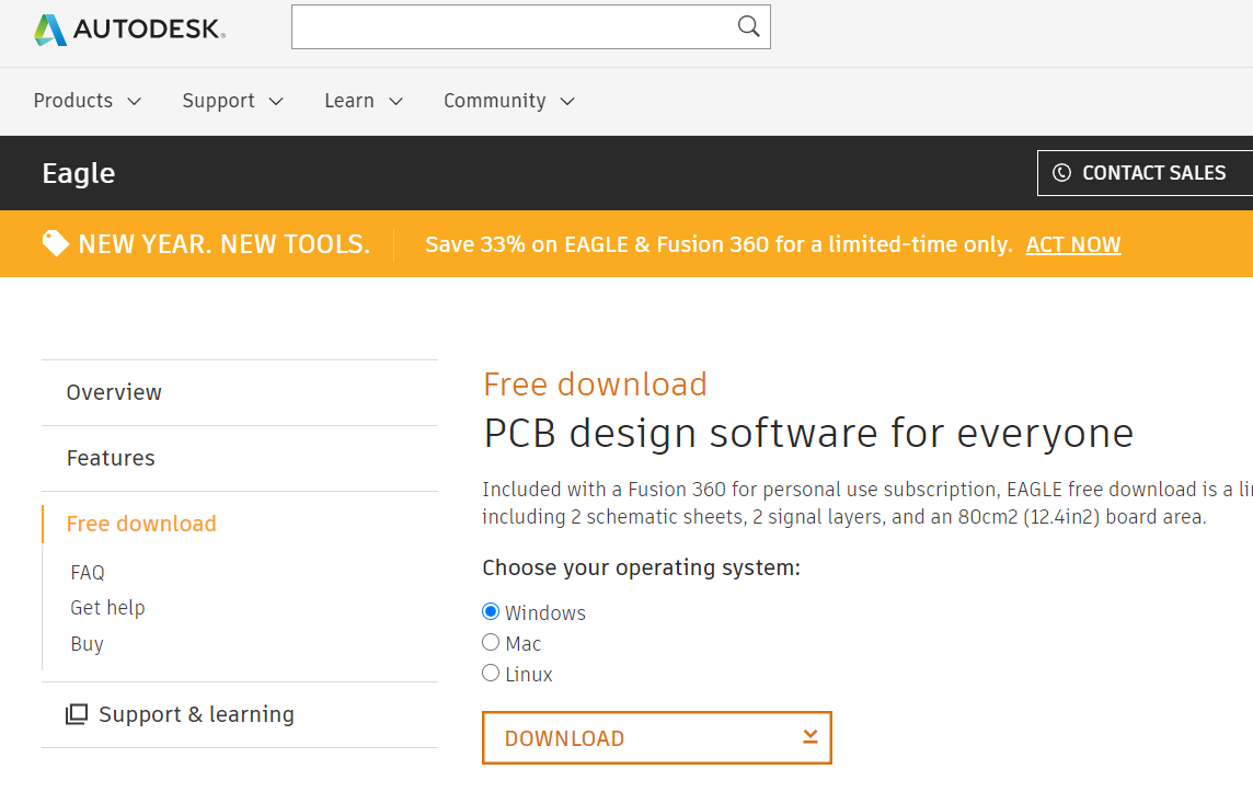
DEFINITION OF AUTODESK EAGLE
Autodesk Eagle software used to design the PCB and it’s defined as a scriptable electronic design automation application with schematic capture, printed circuit board layout, auto-router and computer-aided manufacturing features.
First of all, Download the Autodesk Eagle software to build our circuit board.
After downloading the Eagle, you will be navigating into the Eagle interface that includes few tutorials into how to use the software, thus building your target circuit board.
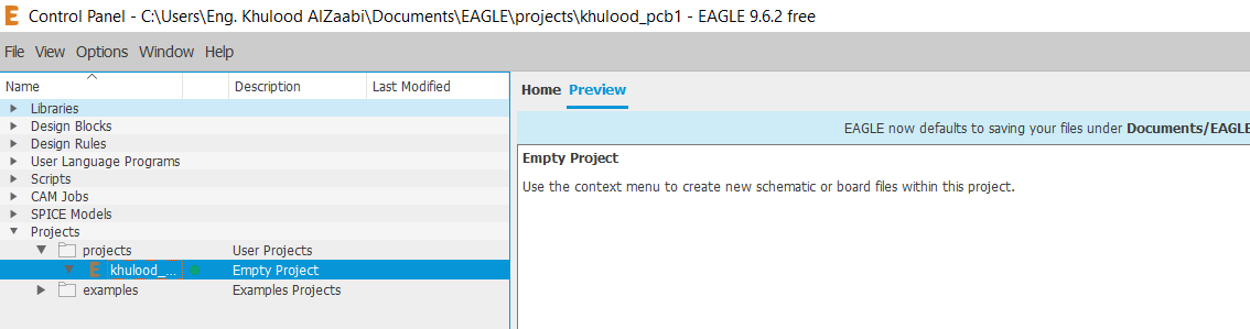
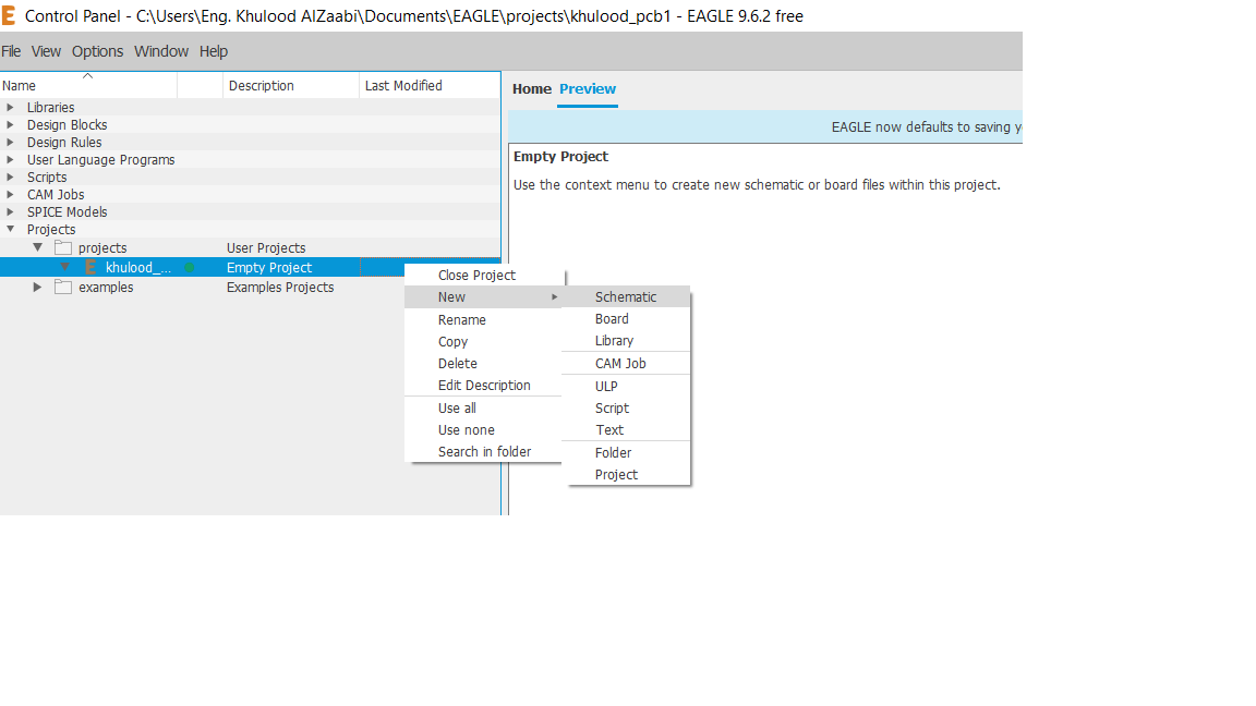
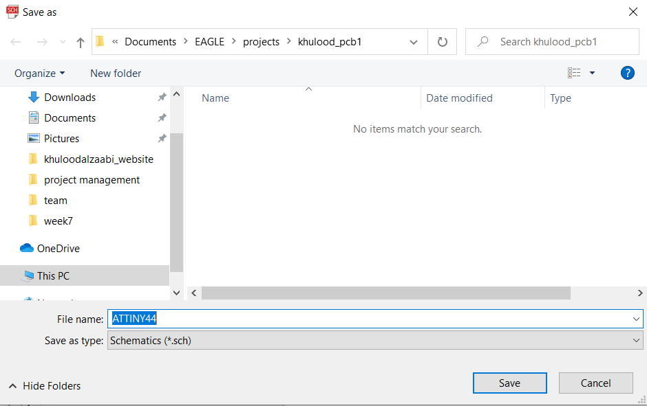
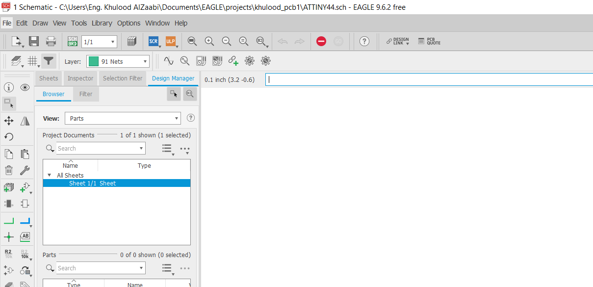
Create a new project, and create a new schematic file to start building our target circuit board. Later on, save it as "Ttiny44", and by deafult will be saving within this path: documents > Eagle
Save it as "Ttiny44", and by deafult will be saving within this path: documents > Eagle
Now, you could start building the circuit board schematic, as shown below.
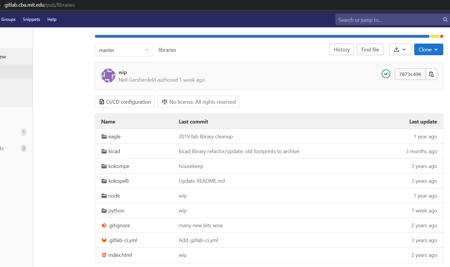
Then we have to clone the Fablab Eagle Library from the GitLab, which includes a bunch of electronic components that we could use in designing our target PCB.
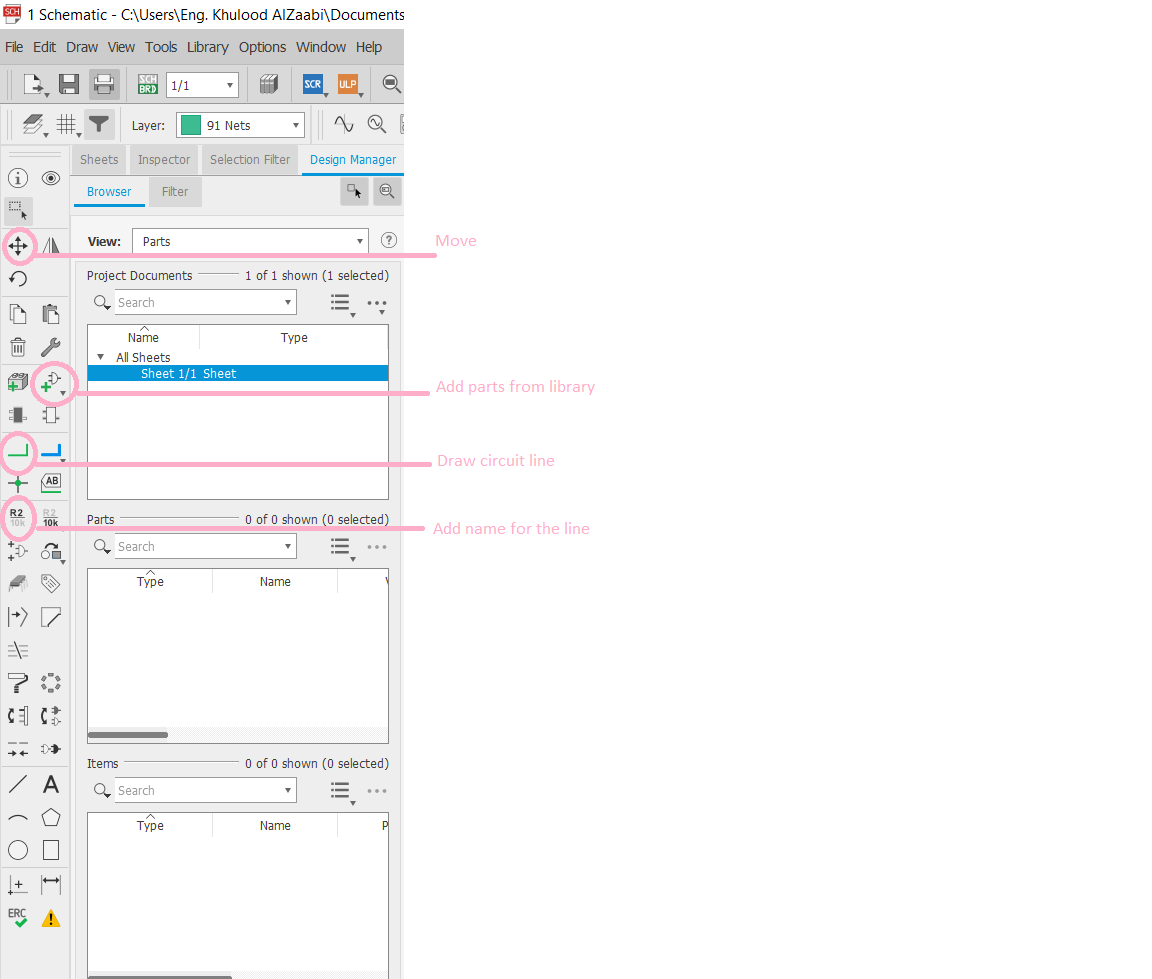
Then, our circuit creation will begin through using the following navigation bar
COMPONENTS TO BE USED DURING THE DESIGN
ATtiny44.
Resistor.
Capacitor.
XTAL Resonator.
FTDI connector (1x6 header).
ISP connector (2x3 header).
INPUT AND OUTPUT TO BE ADDED
Button (input).
Green LED (output) with Resistor.
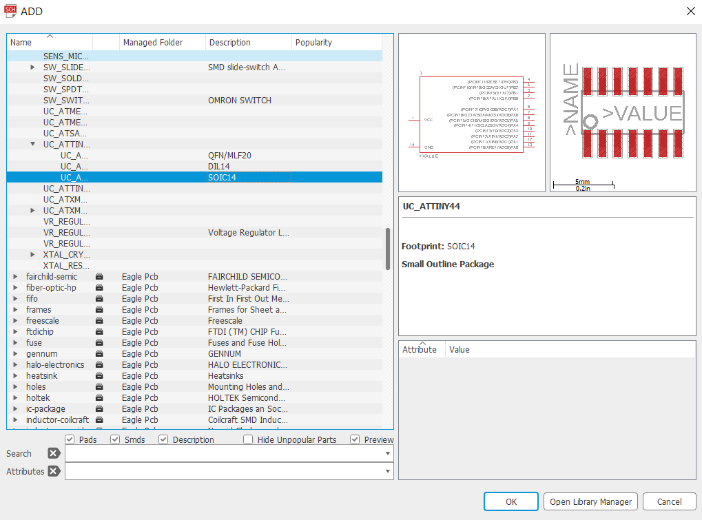
Now, it's a time to add Attiny44.
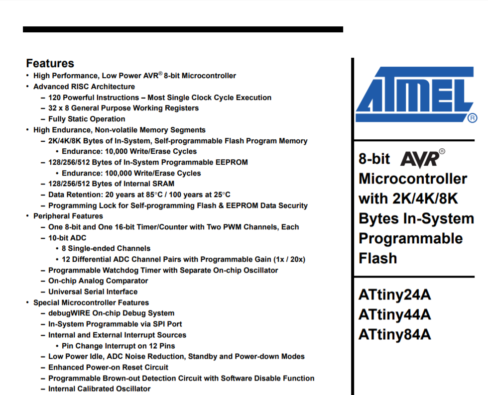
The most important step is to explore further about the Datasheet that explains more about the microcontroller which will be used to design the target circuit board "ATtiny44".
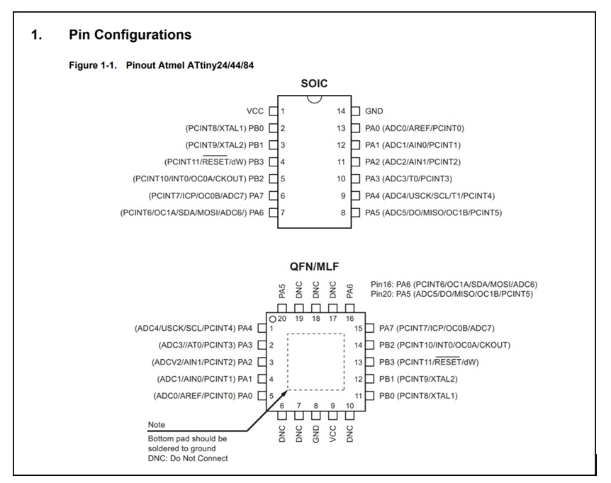
The below image illustrates a pin configuration of the ATtiny44.
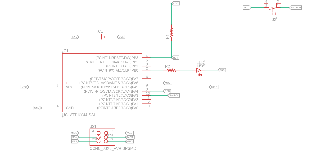
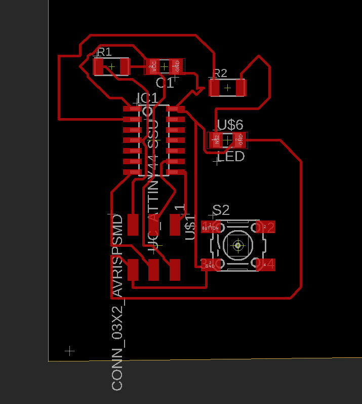
I started to design PCB, including a LED, and other components as I mentioned above on the component section with the purpose of drawing Attiny44 board, with one LED with a current limiting resistor.
.
The following images presents the schematic of the designed PCB.
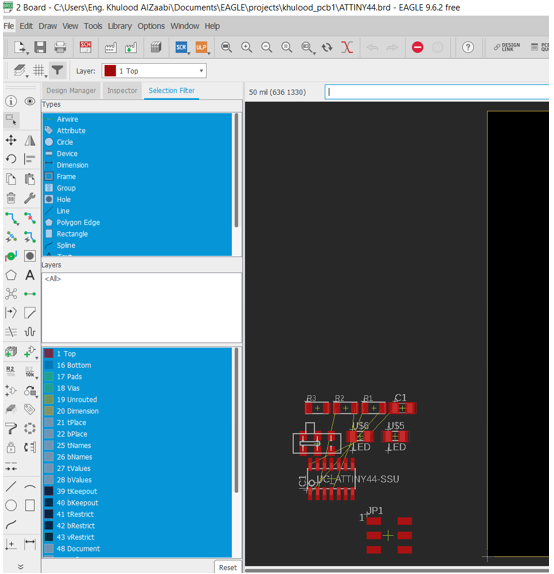
The step that follow creating a schematic is to switch the schematic through navigating into the button on the top left (Generate/switch to board).
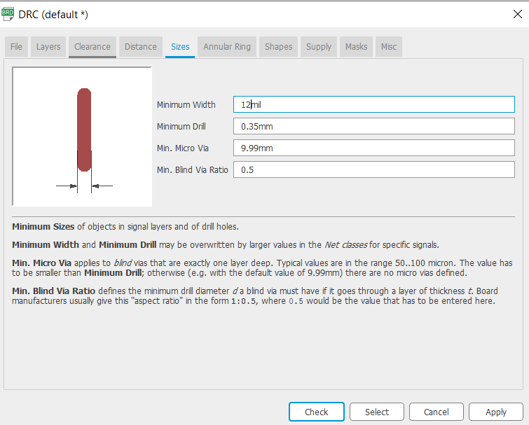
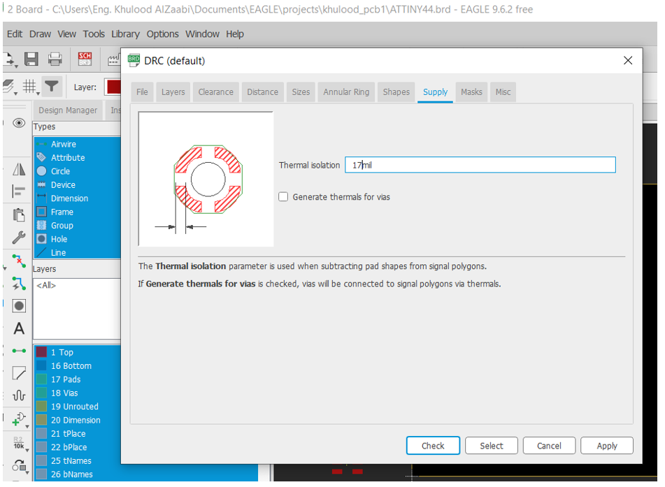
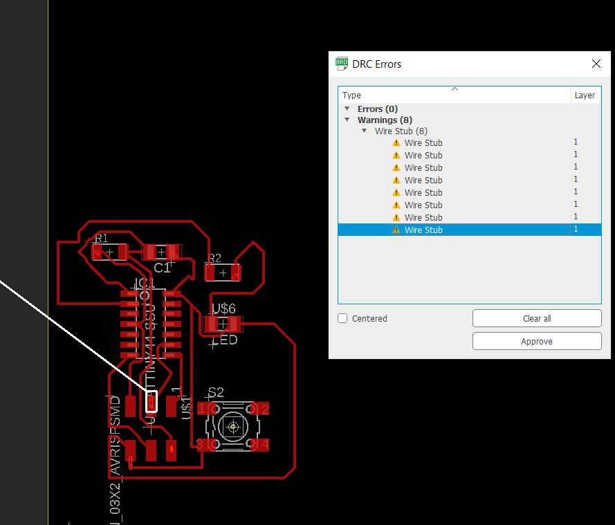
Now, it's a DRC editing (clearance, size, and supply) turn and that's done through navigating to DRC > Clearance (change the signals size according to our milling cutter size “0.4mm”).
In this step, the whole parts should be re-organized and connected together through navigating to use > Route Airwire tool on the left bar.
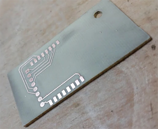
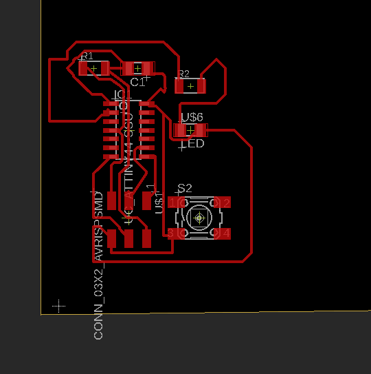
The final board been ready to move into the next phase of electronics design as shown below.
We have to re-check the DRC clearance, and I did get warnings, and one error.
Finally, our PCB is ready to be use for further implementation .
LESSONS LEARNED
1. THE PRINTED CIRCUIT BOARD COMPONENTS
I studied these kinds of course before at University, however, this task as a refreshment to my previous knowledge as I forget the PCB components’ name, and I navigated to read (as an example) ATtiny44 supported document to know further about it, and I searched to be familiar about the component name, thus choosing these components become easy while navigating into the FAB Library.
2. THE PCB'S CONNECTION
I faced difficulties at the beginning while designing the circuit, thus asking Eng. Hashim for his assistance and guidance, until I became familiar about the circuit, and its connection. Also, how I could use the navigation bars, and its tools as an example, move, label, etc.
3. ROUTE AIRWIRING THE PCB COMPONENTS
Most of time I spend it while route airwire the PCB components, as sometimes, the connections’ line hinders from connecting other components together, so I have to fetch for another path. In regards, the DRC warnings and errors, I got warnings as I missed a blocked of connections’ lines and I have to remove them. In addition, I got one error and that’s due to the changing that I did to the circuit schematic. All these obstacles been fixed.