week5
softwares to try:
- Autodesk Eagle
- KiCad
- FlatCAM
steps to design PCB
- first download eagle from autodesk
- open eagle, click in create a new schematic file
- schematic is the representation and usage of symbols and in eagle it is the components you use
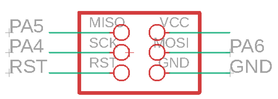
- Atiny 44
- R1 - resistor- zigzag 10k ohm
- C1 - capacitor 1 uf
- XTAL 20 Mhz
- FTDI h
- ISP h
- LED
- Resistor
- Button
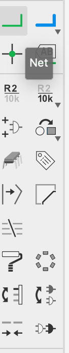
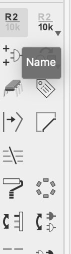
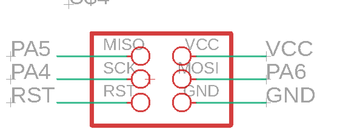
- click on net and then choose the part you want to label
- im doing vcc so i click next to the red circle and make a line
- then click on R2 to label it
- im naming it VCC as shown in the part
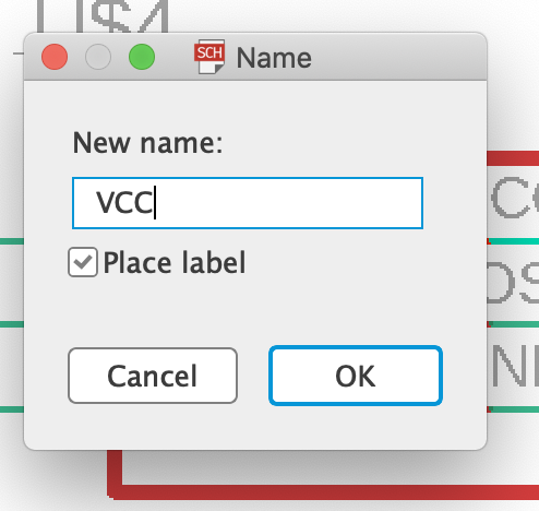
- click yes to connect it to the other VCC which i named VCC too so when you name two or more parts with the same name it connects them automatically
- lastly it will look like this
- connecting the parts by clicking on autoroute and then make sure it has 0 vias

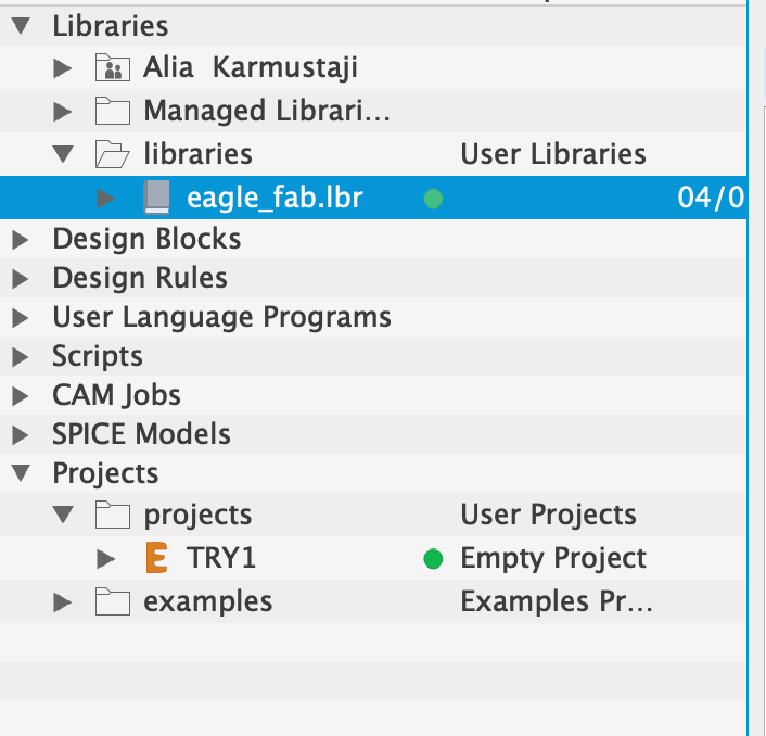
Downloaded the program “Eagle CAD”, then watched few lectures on how to use it and make a functioning circuit board. Yeah Eagle is not a bird but it is an electronic design automation software. This software help you design and print a circuit board easily and smoothly. After downloading Eagle and spending hours watching videos about it. I got the courage to start making my first circuit board. These are the steps I followed ———> 1. Open eagle 2. Go the Fabacademy website 3. Download Fab Library to use in the software 4. Go to Documents click on Libraries 5. Choose eagle-fab.lbr 6. Click on it again in the software and make sure the button turns green 7. i used ATtiny44 for reference as the assignment mentioned 8. I went tot the fab website, I got Neil’s board to use 9.Later I started placing my components 9. After having all my components layed out I organized them 9. I connected the components
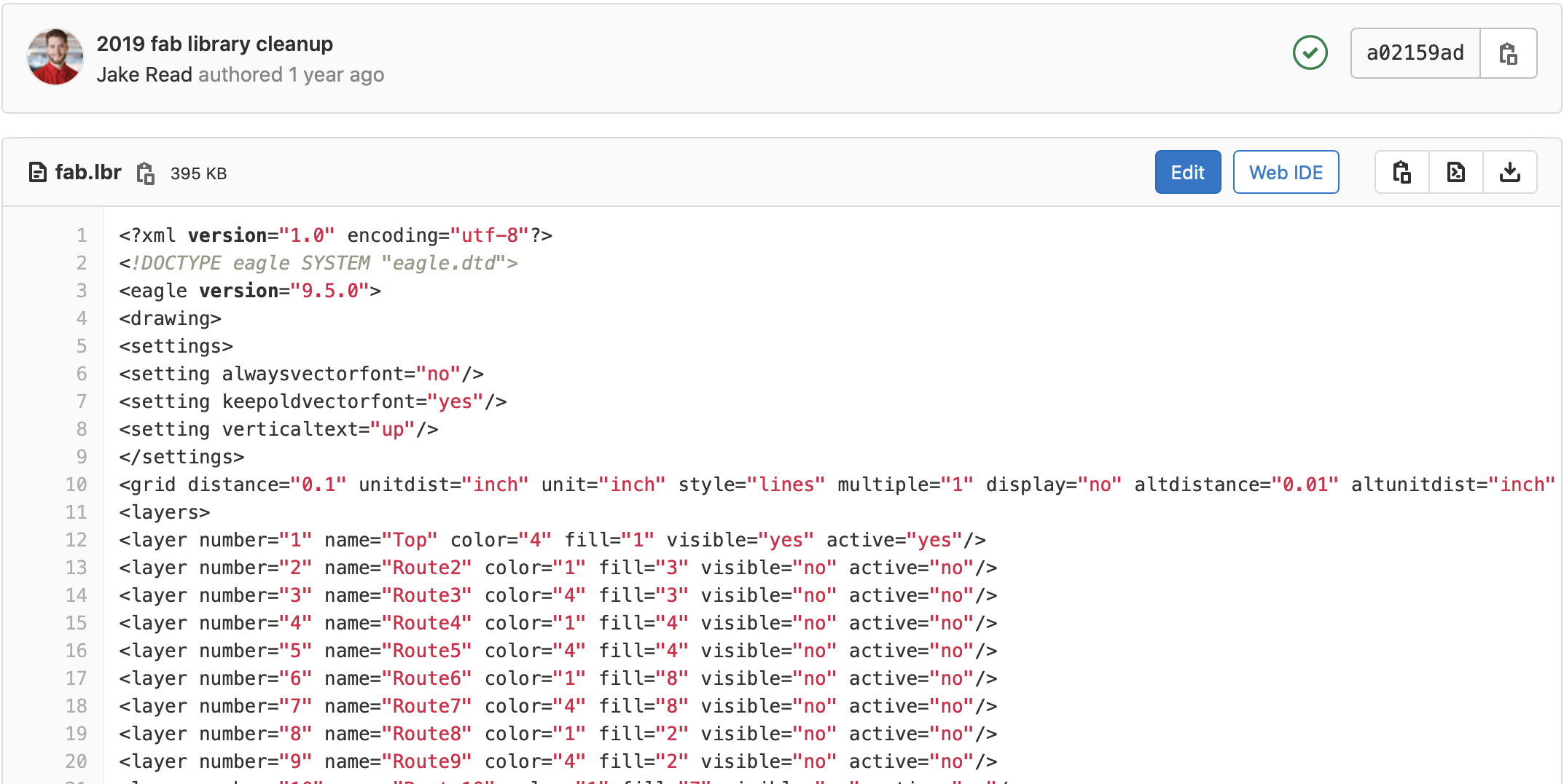
adding fab library, got t fabacademy website then 2019 fab library cleanup.
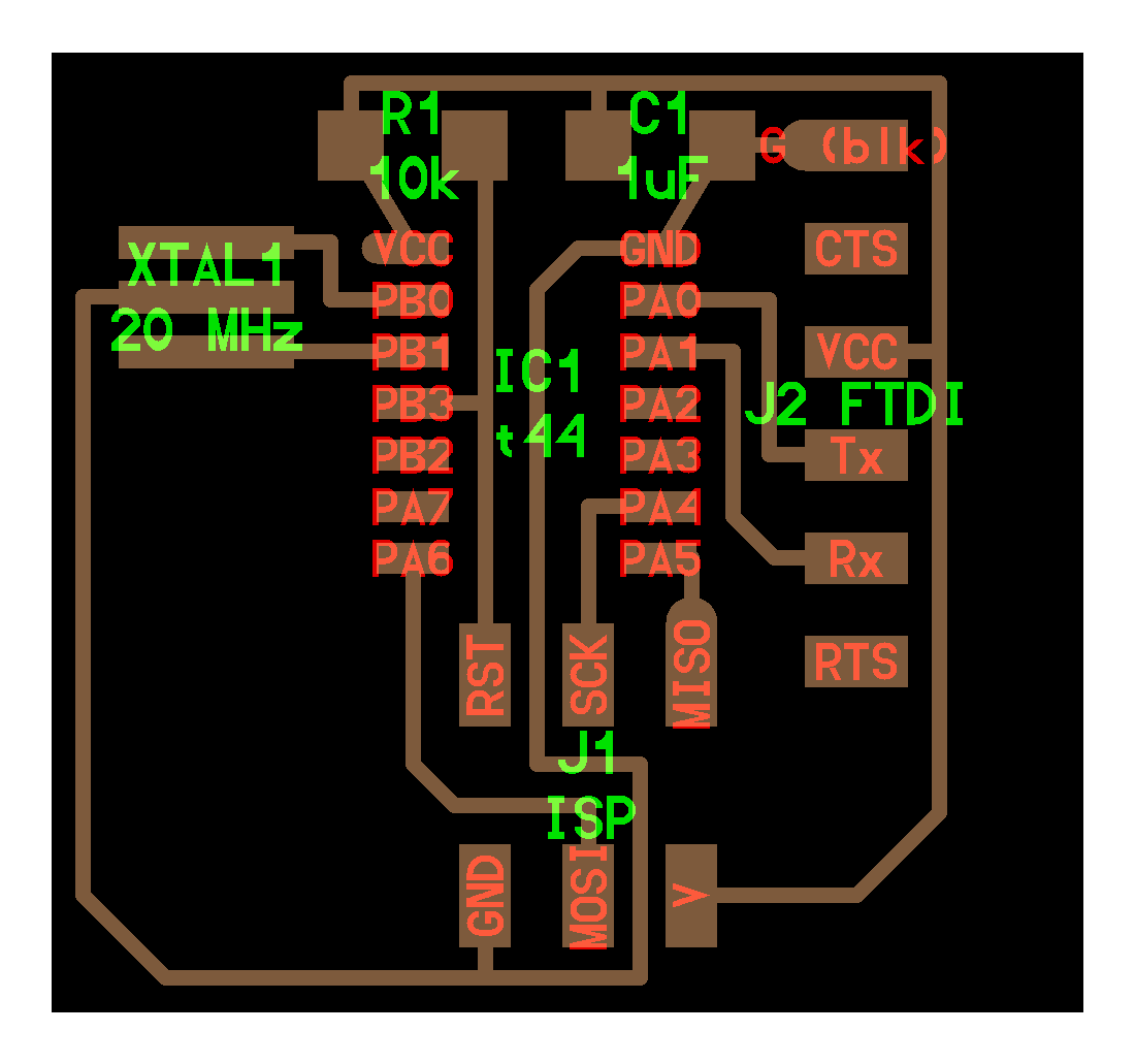
i used this board of attiny55 for reference which i found on fabacademy website
components:
adding the components
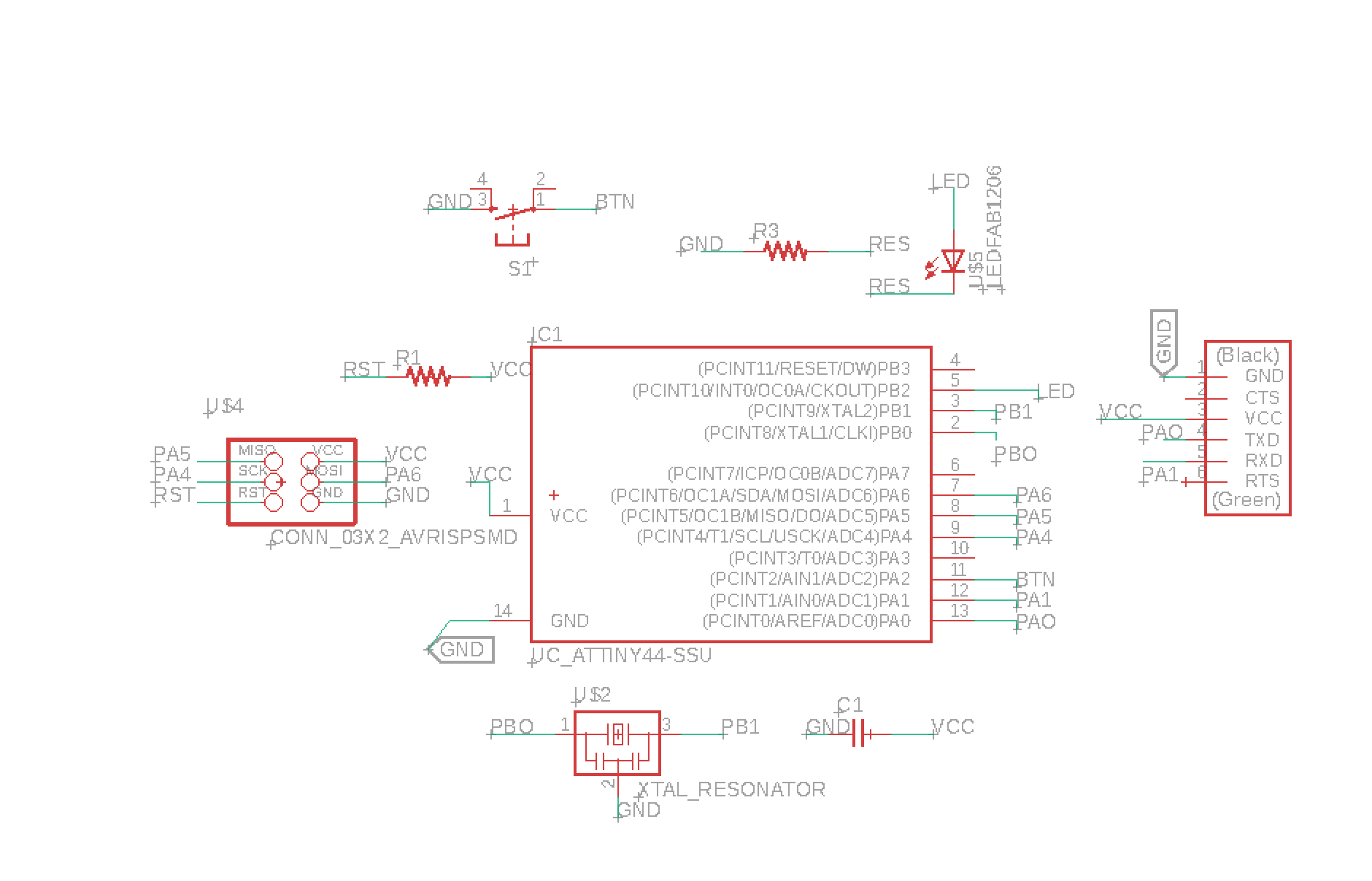
labeling and preparing parts
after adding eveything needed i click on this button to change the file from schematic to board

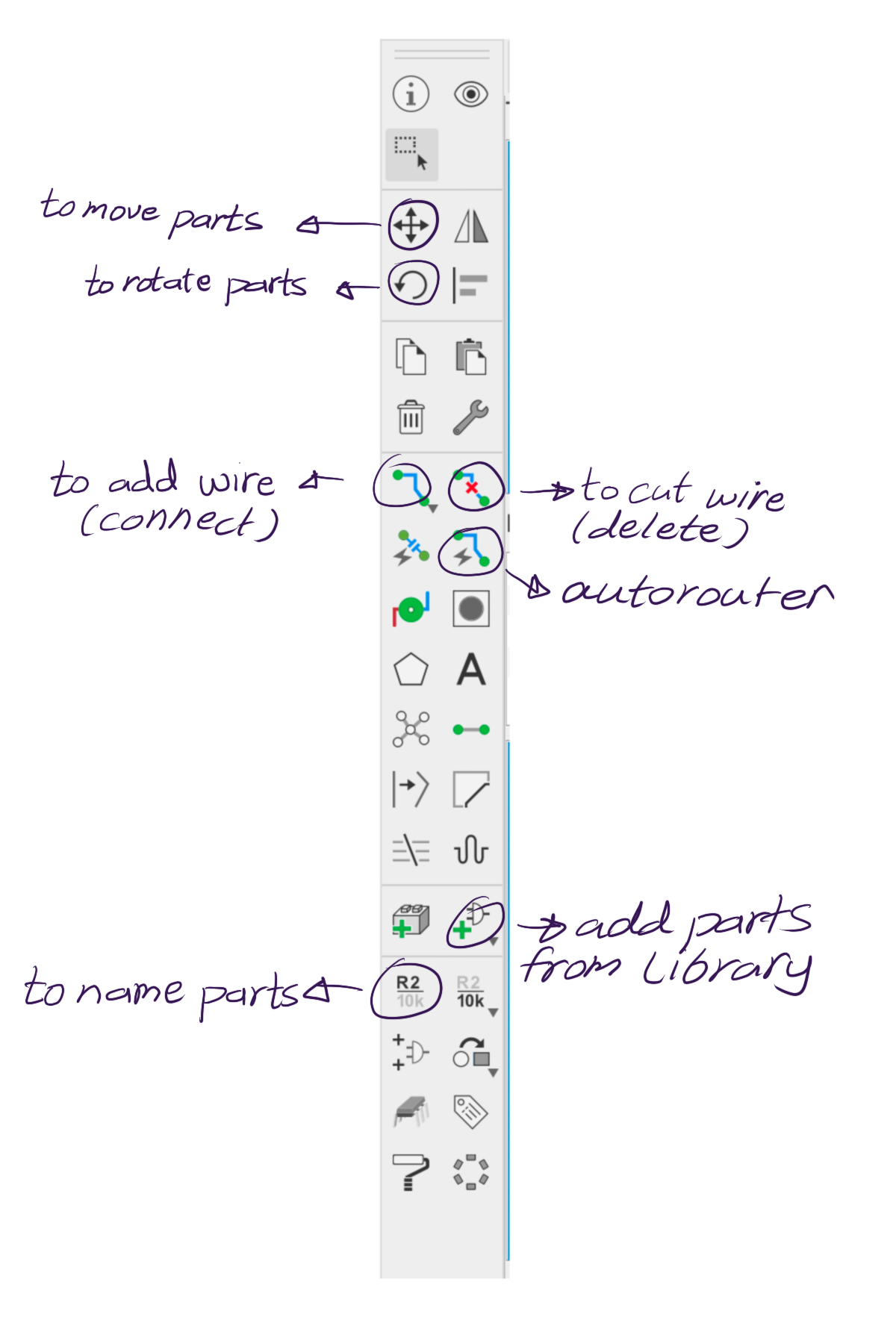
showing what each button do
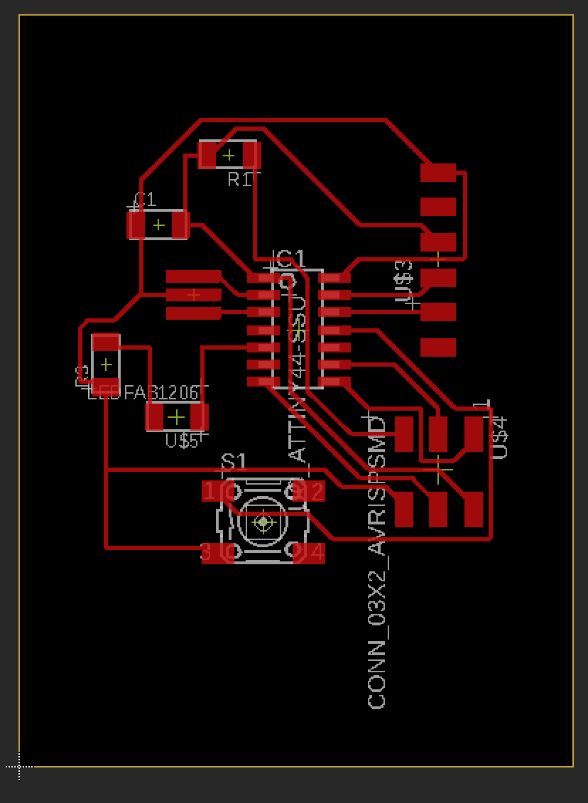
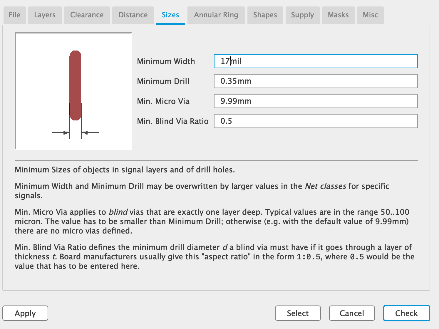
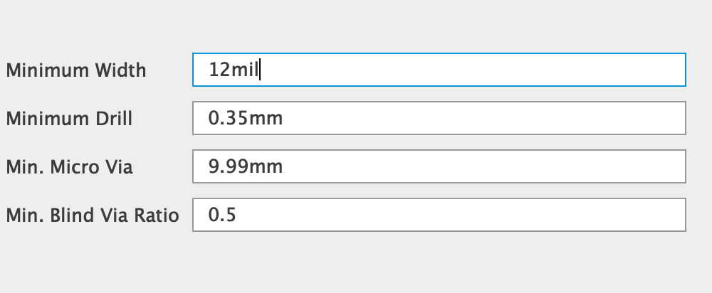
Changes the size from 17 mil to 12because i had a problem with connecting the parts without having to use the back of the board
this is my final board but i need to fix the GND and try another way to connect it
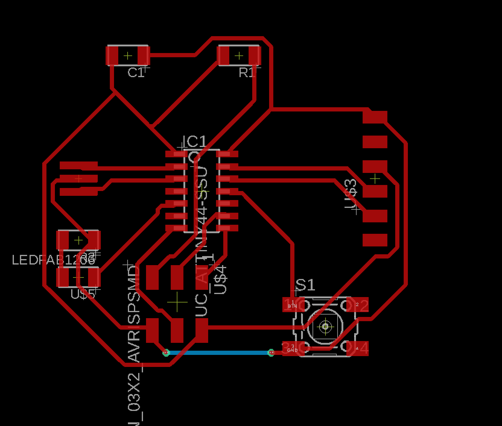
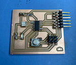
this my final board