Week 6
When you discover a new tiny component but have no idea what's its purpose
Table of Contents
So, we turned back on electronics, so I'm quite happy about it. I didn't really had my fun with the previous week, mostly because of myself, since I'm not a very creative person so I kinda suck when it comes to designing something: I start imagining beautiful things but then I don't have the time or the ability to craft them, and I usually remain with a sense of insatisfaction that sticks with me for a while. Since I realized that I loved the practical part of soldering the pcb a few weeks ago, I know that I'm going to like this week as well - because I'll learn even more about it. It's strange that someone with humanistics background and no knowledge at all of physics, electronics, mathematics, and so on finds herself liking this kind of week theme. I'm very, very bad with number and precise stuff, but ... I'm enjoying this intro in electronics, nonetheless.
I also started again my University Courses, so I'll have to manage my time in doing both things simultaneously - I'll try to do my best to keep up! It seems strange and probably sounds weirder, but I almost forgot during these past weeks that I also have the university going on. It's a nice thing, I guess - it meens I have been totally taken by all the new stuff and even if I'm not particularly good or creative in what I'm doing I'm enjoying it anyway. More than I thought, which is beautiful!
Some notes about Electronics (Updates as I go on)
Electrical Components (Updates as I go on)
Learning about Schematics
.. and about Boards!
Milling
Soldering and Testing
Updates
Download
Objectives
- Individual assignments: Redraw one of the echo hello-world boards or something equivalent, add (at least) a button and LED (with current-limiting resistor) or equivalent input and output, check the design rules, make it, test it.
Preparing for the Week
Software Installation and Other
[4th of March]So, we started the new week with a lesson on Eagle - since in the lab we are all using Fusion 360 already, we decided to stick to it and go on using the Eagle software for this work. I have to say that I was curious about a bunch of other programs as well and I installed Altium - it has a nice Student Plan which gives you six months free trial of the program, the cloud service and libraries. Sadly, my Computer is not strong enough to run the program correctly so I had to disinstall it quite quickly - even though I really liked it on the appearence. It gave me the idea of being more complex than Eagle itself, so I don't know if would have enjoyed it on the long run, but still it might be useful to know for you that are reading this that you can try the six-months plan.
I moved on cloning the FabLab Library on my computer in the repository and I started taking a bit of confidence with the program itself. While Eagle was downloading, I head on to the book-shelves in my laboratory and took one about electronics, curious to study a bit of theory too about all of this. We have a really nice book: Getting Started in Electronics by Forrest M. Mims, that I enjoyed not only because of the really nice drawings and hand-written chapters but also because it's quite informal and easy to follow (up to a certain point, where it gets more difficult for me to follow).
I understood better how electricity works and how to create some basic circuits, at least in theory - which worked better since I had to solder two weeks ago and I remember the importance of the components and the copper paths which conduct energy. I don't know yet what each component dose, but at least I'm starting to create a basis on which I can work on from now on. Sometimes I also like to take a board from the ones that we have in the laboratory and look at it, trying to understand why some components are displayed in a way instead of the other - and I know I'll understand more about this when I'll start doing the layout myself. Can't wait for it!
I also started to read some stuff online to better prepare for this week, integrating them with what our Instructor Simone explained us about the two-steps-flow of creating a PCB on Eagle. First you have to design your schematic and then you work on the board based on that same schematic, preparing your PCB - these two editors work hand-to-hand. A well-designed schematic is very important to the entire process, because it will help you catch errors before the board is fabricated so you don't waste materials and precious time. One wonderful and powerful guide and tutorial that I followed later on in the week is available on Sparkfun and I think it's really welcoming for beginners. It has a lot of information, screens and further things that you can discover as you go on. I'll probably try to follow more of it in the days to come.
Some notes about Electronics
About a Communication Student who approaches Electronics
I took some notes from my study, because since I have a humanistics background I really find it difficult to keep up with all the beautiful things that I see and that are made by students that come, most of the times, from scientific background. I would like to know what I’m soldering, why am I using them instead of others, how does all of this work and so on, and I’m perfectly aware that the material is a whole lot more than I have studied now. But still, I have to start somewhere, and usually you start from the basis – so I’ll write down some things that are useful for me to remember and write down but might be also useful for who is reading all this. We are working on circuits, as we have seen during Week 4 and we are during this one. A basic electrical circuit has some characteristics such as the different things that make it work:- We have V, the Voltage (measured in volts). It usually is a battery, which has different electric potential from one point to another, which is why you have a minus on one end and a plus on the other one;
- We have I, the Current (measured in amperes). It’s basically the flow of electrons which move from a point of the circuit to another.
- Lastly, we have P, the Power (measured in watts). This is, as the name suggests, what gives power to the circuit, it’s the electrical energy that is transferred throughout the system.
So, for a circuit to work well you need at least the source of power, which might be quite obvious to write down but you can never tell things too much when you're approaching a new field of study. I have done some maths, physics and so on during previous years of high school but I never actually liked it nor I had good teachers, so I studied for the grades. As you can imagine, I not only studied them badly but I also forgot them, and I never actually developed a schematic, logic and linear, matematical way of thinking - therefore, I usually tend to have difficulty with these things because I'm hasty. The reasons why I say this are mainly two: the first one is because you don't know me and I want you to, in order to better comprehend why I write certain things and why I make the mistakes I made; secondly because I want to write down more and more as I go on through the weeks, because I realized that I tend to forget things quite easily and if I don't write them I loose them. And, lastly, I take more notes than I write here, but since this is my word against others, I'll try to sum some things up here so I'll also pratice my english on the matter. So, if you're still here with me, thank you for reading all this and let's go on!
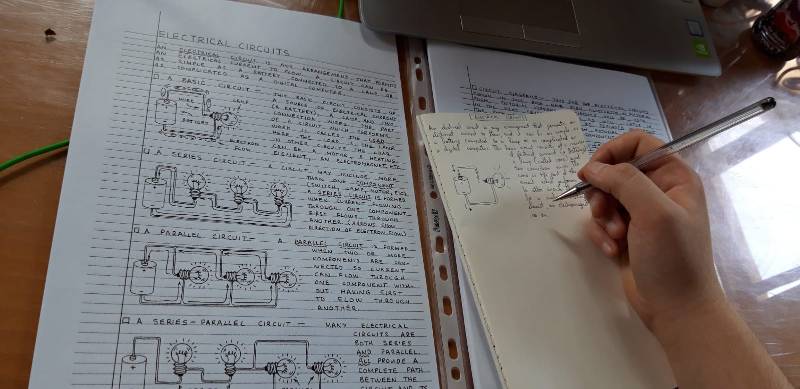
Electrical Circuits
The book has some beautiful drawings about circuits and the basic types of them, but in general it states that circuits are "arrangements that permit an electrical current to flow". So it can be a very simple circuit, with a battery which creates a different quantity of electrons and is eventually connected to something such as a lamp, or it can be very very complex such as a computer. Usually in a circuit you have something which performs the work and it's called Load, in the case that I mentioned with a lamp and a battery the load is the lamp itself but it can really be everything, from motors to electromagnets and so on. Circuits have diagrams, you can draw them and use some symbols which are universally used to indicated all the components that you might need: these can help you approach this field and understand things from basic to complex, even before moving to drawing digital schematics and boards. The principles are, obviously, the same.
You can have:
- Series Circuit: which has more than one components, so for example as we had to do for this week you might have a switch, leds, lamps, motors, and so on. We have a "series" circuit when the current in order to flow to a component it first has to flow through another one as well, and you usually indicate this with an arrow if you draw it;
- Parallel Circuit: which is when you have two or more components connected, but they are connected in a way that does not require the current to flow firstly from one component in order to arrive to the other one;
- Series-Parallel Circuit: this one is quite complex on paper, but it becomes easier to understand when you go on Eagle (or a similar software) and you start drawing yourself. Its usually a complex path witch is both series and parallel, as the name suggests.
You can in general have two main types of current electricity in a circuit, which are AC and DC: the first one is the Alternating Current, usually rappresented as a sine wave, which is when a current alternates its values in direction or polarity (which is the intensity, if I'm not wrong); and the second one is Direct Current, which as the name suggests it has always the same linear current. You can measure both AC and DC voltage with the Multimeter - as we learned during the group assignment. I'll eventually come back to this concept later on.
Electrical Components
You have a lot, like really tons of components in electronics, some of them are more important than others and I will not talk about all of them - but I'll try to write down at least some of the components that I used most, but I'll not use a specific order. You have to know that there are a lot of different types of the same component, depending of what you're going to do with it, what you are needing it for, and who is the productor that realizes it. I'll update this section as I go on and descover and study new components.
Resistors
Resistors really have a lot of shapes and sizes, colors and so on, but they all have a singular purpose: limit current, for example I used a resistor with the LED in my PCB in order to regulate the current flow. They are measured in Ohm.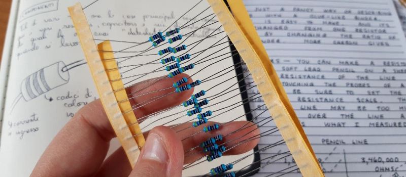
The book also states (I didn't notice nor payed attention at first) that resistors have different lines of colors which indicate the resistance of the component (and its multipliers), and Simone told us that sometimes you can also substitute resistors if you don't have that precise one. For example, if you need a 499 Ω resistor, you can safely use a 500 one.
Something more about Resistors in the Update section.
Capacitors
Capacitors have a lot of types and sizes as well, since I showed you one type in the previous photo, I'll show you another type now. Capacitors store electrons, and the simplest one is made by two conductors separated by an insulating material called "dielectric". When I selected my Capacitor for the PCB I didn't think about the measurement it has, but then I started wondering why it's calculated in Farads (F). Googling a little bit I found out that it's the unit for "capacitance" and it works in relation to the amperes as well (tho I have to read this a hundred times because I still didn't get it). I used this Dummies Reading about the argument.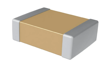
I used a capacitor for my PCB, I used the components that were present on Niel's schematic but I went by faith, taking the components that were written there, selecting them, placing them and routing them. I wanted to learn more about why they are there and how they work, so since at first I didn't understand why there was a capacitor if it was connected only to vcc or gnd, now I better understand that ... well, it's its purpose to be that way.
Eagle: Learning about Schematics
[From the 5th of March to the 7th of March]When you open Eagle you find yourself on a blank page with a column on the left, where you can start New Projects - you might want to create one for each PCB you're going to do, in this way you have a really clean and ordered series of boards. I found it easier this way, since a mess a lot when I try to figure things out so I create and abbandon projects, create and ruin them, and then create again - so if I have different spaces at least I can delete stuff without worrying too much about the possibility of cancelling something useful. Although I'd never advise someone to work like me, so if you do, I warned you.
You can download libraries online and have different kinds of components and graphics for your schematics and boards, which is something quite nice once you take hand with these things. I activated the Fab Library and you can see it active when it has that green dot on it, but you can and might have multiple libraries - it's up to you. Once you prepared all the libraries that you want and once you created your Project folder, you can right click it and create a New Schematic - this will be your first step for the creation of the PCB Layout. A new white window will open up (beware that if you close the main one the others will close too) and you then will be able to select manually all the components that you need and drag them on the workspace.
At the beginning it's quite messy for someone who has no idea at all of what they're doing, but don't lose hope - if you look at the sampe echo hello-world boards and note down each component, you'll eventually be able to find them in the libraries and drag them on the workspace. I personally checked every photo multiple times and after a few tries I started to remember the most common folder used in the Fab Library for these simple starting boards, so it's really just about getting a bit of practice with it. Once you have dragged and pinned down all the components that you need, you can start thinking how to connect them and have a general idea about what you want to create. You can use different types of methods, either connecting each pin with the correspondent other one with the Net button or labeling the single pins for each connection that you want. So you can choose to have a network of green lines that connect everything like this:
Which might be useful to start getting an idea on how you will need to arrange the space later on in the Board-step of the work and also gives a clear visual rappresentation of the interconnections and dimensions of the entire work. Or, you can also try to name the labels of the connections that you want to do, by using the "Name" function always on the left, and do something like this:
As you can see it's not mandatory to use only one of these two methods (and probably there are other ones as well), you can mix them and have fun trying to understand which one is better for you. I have to admit that I enjoyed the second one the most, because it gives me the illusion of being an ordered person, but I quickly changed to using both of them when I realized that most of my work didn't work out in the Board-Session of the work.
Eagle: Moving on to Boards
Once you finished with the Schematic and you're happy with the result, you can move to the top where you'll find a button (it's either slightly green or red) which will allow you to Generate/Switch to Board (or viceversa). Here you initially find all of your components with a different graphic than before and you'll see messed up in the left-corner of the screen. You'll have to drag them in the black workspace, but our instructor adviced us to do some steps before starting to work and connect all the pieces together. Some of those advices were about doing two main things:
- Setting the Grid: This will be useful to check and keep under control all the work that you do, the spaces between the traces that you'll draw and the components. This is the part where you literally draw the traces that will be made of copper in the final result so it's important to consider also the physical limitations of space and work while soldering.
- Defining the Design Rules: This is important to set because you also have to be aware of the dimension of the drilling bit that the machine will be using to carve or cut your PBC - in our particular case, we modified some of the parameters as for the tests that we did in the laboratory.
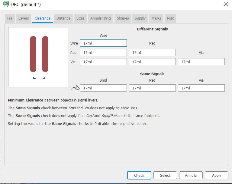
As you can see, I changed the Clearance parameters from the default six to seventeen - but you might also want to check, for exemple, the Witdh of the traces you'll draw - mine are setted on ten. We'll see if its enough, I hope so.
Creating my PCB
Making the Layout and preparing for work
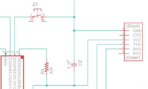
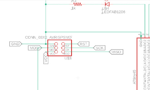
[Week-End]I started working on my PCB layout using only labels and names to connect the different parts, and I thought I made a nice and beautiful work, but it didn't work well when I moved to the Board as I wasn't able to connect everything properly. I tried in every possible orientation and it still didn't work, so I decided to start all over again - as I usually do when something decides it doesn't want to function. I prefer to begin the process from scratch rather than wasting hours trying to convince the previous job to work. At the end of some tries, I had this result:
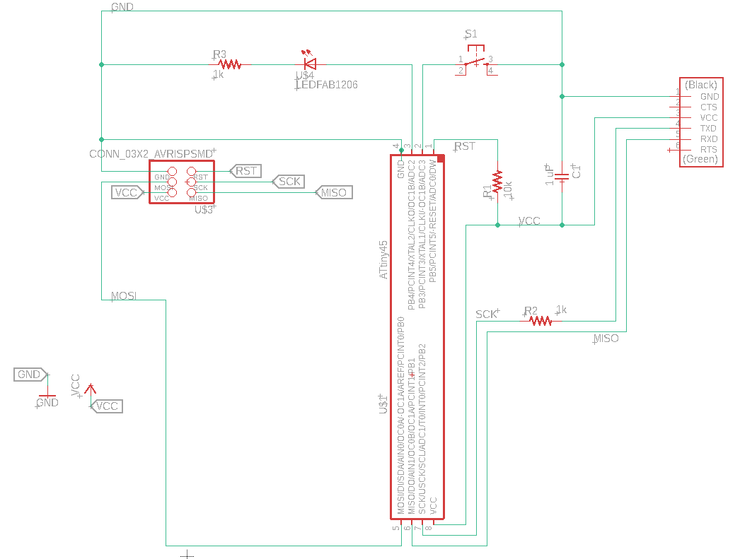
I had quite a lot of fun with this part of the work and I think it turned out quite clean; I'll try to do these things again in the days to come, because I'd really like to learn how to do them properly. I've seen some sites about how to do schematis in a cleaner and organized way but I don't really have that much of components so I think it might be ok for the time going such as it is. I took all the components from the list available on the Fab Schedule for ATtiny45 and then added a LED and a Switch. I then moved to the second part of the process, the Board.
Board-making
After doing my Design Rules (which you can find up in the previous sections) and calibrating my Grid, I started to drag all my components to the black workspace. I first tried to cheat using the Autoroute function on the left side of the panel, but I wasn't really happy with how it turned out and it had some routes going on the "Bottom" layer and I didn't want this to happen. I cancelled it and started to draw it by hand, trying to rotate che components as I thought was better to create enough space for everything.
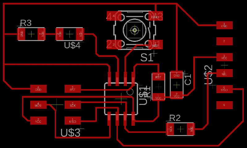
For this screenshot I removed the grid because I wanted to do a nicer shot of my work, but you should consider keeping it on all the time when working even if you sometimes remove it to have a better look at the whole work. After checking that everything was in order I had to check for Errors and fortunately I had none, I checked also the width of my traces and I selected them to be 10mil - hope they'll be enough, even if probably they'll turn out too thin. We'll see!
The important thing now is to hide all the levels except for the top one - you'll get a neat and nice image with only the red traces, without anything else (nor even the writings or things like this.) You have to export this image as a png and monochrome, remember to check where you save it because I lost it in the puzzle of my computer folders and even if it's not a big deal I lost my ten minutes around it. Once you created your file png, is important to open either your Gimp or Photoshop (or similar programs) and prepare the two important files that you're going to need for the machine to mill your board (as we did in Week 4).
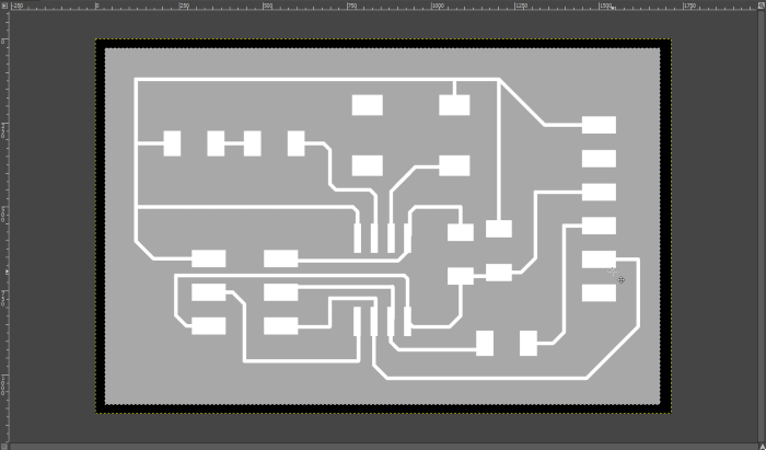
You have to create the cut and the mill files for the machine, you can do it on the program - I forgot to let the dimensions from Eagle so I had to create them on Gimp, but it's not particularly difficult. You cut the image of the dimension that you need and remember to consider the physical space you're going to need for this, specially when you're doing and preparing the external outline. As you can see in the image, I created another level on the traces one, I lowered the opacity so that I could see all the time the image underneath, and then I made my outline ... line (sorry) with the reassurance that all it was going to fit. After all this, I created my files - which you'll find the Downloads section - and launched them on Mods in order to have my .rml files. I'll have to wait Monday to make it, but I hope it's all well done.
Milling
Back to work!
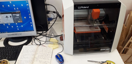
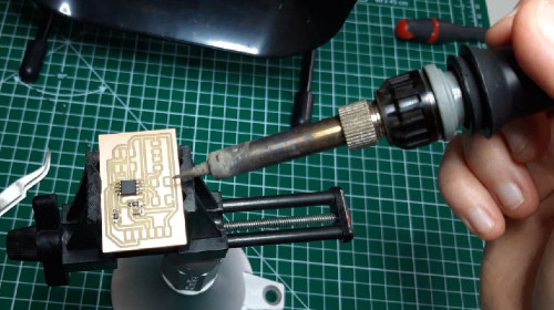
[8th and 9th of March]As soon as I finished my files I went to Simone, our Instructor, to check if everything was in order according to him - I also had no Errors at the end of the work in Eagle (and those that I had before I fixed them going on). We moved on to the machine, after using Mods (you will find a quick "tutorial" to Mods in my Week 4's documentation) and then I started the milling process. I always have a bit of worry when using this machine because of how we nearly broke the machine a few weeks ago, and at the beginning I realized that the drilling bit started to mill "in the air" without actually touching my copper board. It has been told me that this happens if the drilling bit is too short, so I'll have to remember to keep it a little bit longer and don't worry about it. I actually wasted half a cm because when it started to work I was worried that it didn't take the right dimensions and stopped the machine - but I later realized that it would have been ok, it simply moved elsewhere to start it's work. So if you do see the drilling bit going elsewhere and started working, don't worry at leave it do - you'll see that it actually knows how to do its work.
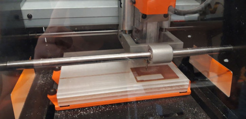
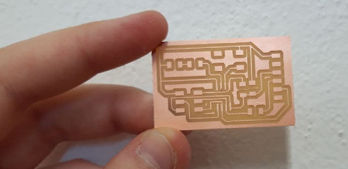
I prepared my notes to keep track of all the important things to know when setting the X/Y asis and the Z one, the changing of the drilling bits and so on. I launched the machine for the traces first and I used the same copper board that I had left from Week 4, the "Size difference" between the board made a few weeks ago and mine is ... quite huge. But I eventually fell in love with my first PCB!
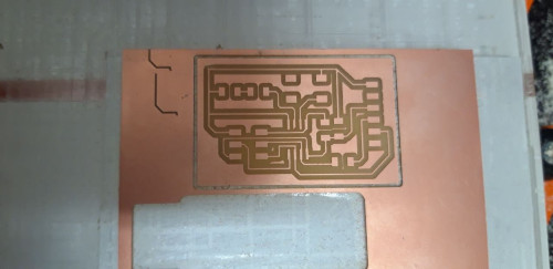
As you can see, there are two lines on the copper board, in the image on the left: those are the two times that I started to mill the copper and panicked that maybe I setted things wrong, so stopped the machine and started all over again. At the end of the journey, I can say that it was right and I could have let it work and do it job without any problem, I'll have to deal with my anxiety of getting things wrong - because it will happen even outside of my control over things.
Pay attention: I had 10mil Width of the Traces, and these turned out really really thin - I didn't have problems at all but you might want to consider changing the Width on a higher value to have better traces.
Preparing the Bill of Materials
Finishing this, I stayed with Alberto to help him with his milling process - he doesn't really have a good relationship with this machine so most of the times something happens when he's at work with the milling machine. He had to mill the same copper board six times to make it actually work but in the end it turned out nicely! I already moved to the soldering process after he finished milling, firstly because we have only one soldering station so we have to take turns and secondly because ... I really waited for this moment. So, first things first, I prepared my materials:
| Name | Quantity |
|---|---|
| ATtiny45 | x1 |
| CONN_03x2 | x1 |
| 10kΩ Resistor (R1) | x1 |
| 1kΩ Resistor (R2) | x1 |
| 500Ω Resistor (R3) | x1 |
| 1μF Capacitor (C1) | x1 |
| LEDFab (mine is orange) | x1 |
| Switch (S1) | x1 |
| FTDI | x1 |
Once you prepare your bill of materials, you can move to Soldering. I always checked my Schematics while working because I didn't want to ruin things and I quite liked the beautiful lines of my PCB and didn't want to make too many mistakes. I took all the materials from the shelves and was ready to work.
Soldering and Testing
Fun time - "I want to Solder everything"
After preparing everything, it was time to work. I had the opportunity to try different ways of working already in Week 4, in order to try the best position for me to be firm and don't shake my hands too much. I managed to find my personal way of working, using a chair with high arms and the support for the PCB to keep it still while I'm working. With a chair with high arms I never have my elbows free in the air, so my hands shake a lot less - while if I work directly on the table I keep a really, really bad position with my back and neck so it really is not a thing for me.
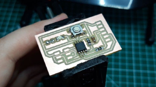
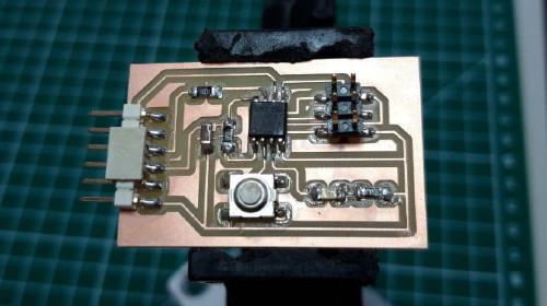
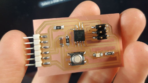
This is how I worked, I washed the board with a little bit of alcohol at the end of the solder process, in order to remove most of the imperfections that it had. I'm quite happy with how it turned out, I know that I don't solder particularly well but I made some improvements from the first time two weeks ago. I learned how to fix the components and not burn everything, and I have to say that part of the reason why I'm enjoying soldering so much is that it relaxes me. I really enjoy preparing the working station and starting to solder, to create the bright silver color that usually indicates a good work and trying to do everything without creating a mess.
At the end of the day, Alberto took a photo of me looking at my PCB in order to find imperfections or maybe some things that could cause some problems in the testing phase. And we started laughing because it almost seems that I found a particular ring of power - so you could hear a "My precious" voice in the background as time went by.
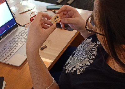
Then we moved on to try to test that it works. We took some time in the laboratory to do the Group assignment as well and we tried to work a bit with all the equipment. You will find more of this on our group page, so be sure to go check that out as well!
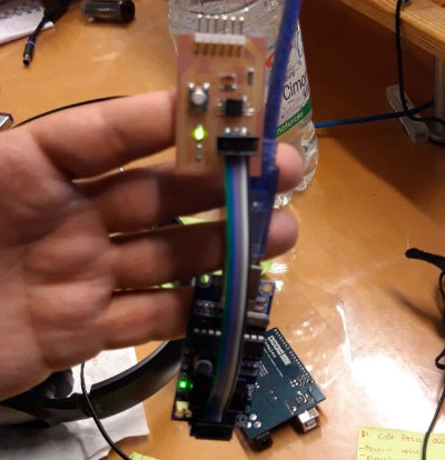
And this is the LED working! I'm quite happy that it worked at the first try, it means that I didn't make mistakes in my work and soldering process so I'm quite happy about all of this week's assignment. It's been one of the weeks that I enjoyed the most, along with the Laser Cutter one and the other Electronics that we made, so I can't wait to see what the new week is going to bring us.
Updates
[11 of March]
- On Pull-up Resistors:Today we had a lesson about embedded programming and some things came up about our work with the PCBs, involving in particular what I had on mine. During our regional review three days ago, Antonio from OpenDot told me that I should have a resistor connected to my switch. At first, I didn't understand why I needed it, but the topic came up today when we discussed about the pins of the microcontroller. I checked a beautiful guide about this subject, which you may find on Sparkfun | Pull-up Resistors, and I wanted to write it down here is someone might find it useful as I did. I didn't write it up in the Electronics section or the components one, because I want to keep track of all the tiny little things that I find and learn here as a sort of "detail" section. It's more useful for me, and I think it's also less boring for who opens my page.
Download
Outline.png file
Outline.rml file
Traces.png file
Traces.rml file