
Week 6 - Electronics Design
Assignment
group project:
      use the test equipment in your lab to observe the operation
         of a microcontroller circuit board
individual project:redraw anecho hello-world board,
      add (at least) abutton andLED (with current-limiting resistor)
      check the design rules, make it, and test it
      extra credit: simulate its operation
Re-draw an echo hello world board
This exercise involves the following 3 stages:
1 - Draw a schematic for your electronic circuit
2 - Arrange the components into a PCB design
3 - Export the design as a PNG
4 - Use the Roland CNC to mill the traces and outline
5 - Solder on all the components
6 - Programme the board using our ISP programmer from week 4
EasyEda vs Eagle
I've previously used EasyEda for circuit design. Although it took some time to get my head around this software, I got there in the end and I'm very comfortable with it. I was unsure whether to try using Eagle or continue with EasyEDA. The main pros and cons were:
EasyEda:
Pros - Easy to use, ideal for Chinese production, free license
Cons - You're tied in to a particular supplier for production, unable to directly link with your CAD models
Eagle:
Pros - You may be required to use this when working with others who use Eagle, you're not tied in to a PCB supplier, you can link it with your CAD models so that the size and shape of your PCB is based on your actual CAD model.
Cons - Paid license, less intuitive to use
Based on the above I decided to try Eagle. I found it very frustrating to use. Compared to EasyEDA it was way less user-friendly, not intuitive at all and I had some silly issues with the installation that meant my icons were not displaying.
On reflection I think that EasyEDA might be a better choice. It occured to me that if I made a PCB in Eagle and then wanted to have it manufactured in China, I would need to open the file in EasyEDA (or similar) and then change almost every part to ensure I was using something that was both in stock and available for their SMD surface.
If I did things the other way round, it would make a lot more sense. You could design a file in EasyEDA making sure to select the exact components you'd potentially want to buy for your board. You can then export your schematic or gerber file and open in Eagle. At that point you can use the link with Fusion 360 so that you're working on a PCB that fits perfectly into your CAD design.
I'm glad I persevered with Eagle. It feels useful to be comfortable in both of these programmes because they both offer some unique benefits. The most valuable takeaway though is that I should be mindful of how long I take to learn a new programme. I think I take longer than most and I found it very frustrating when I was struggling to do things that I knew perfectly well how to do, but in a different programme.
1 - Draw a schematic for your electronic circuit
My schematic circuit is based on the following ATTiny44 board:
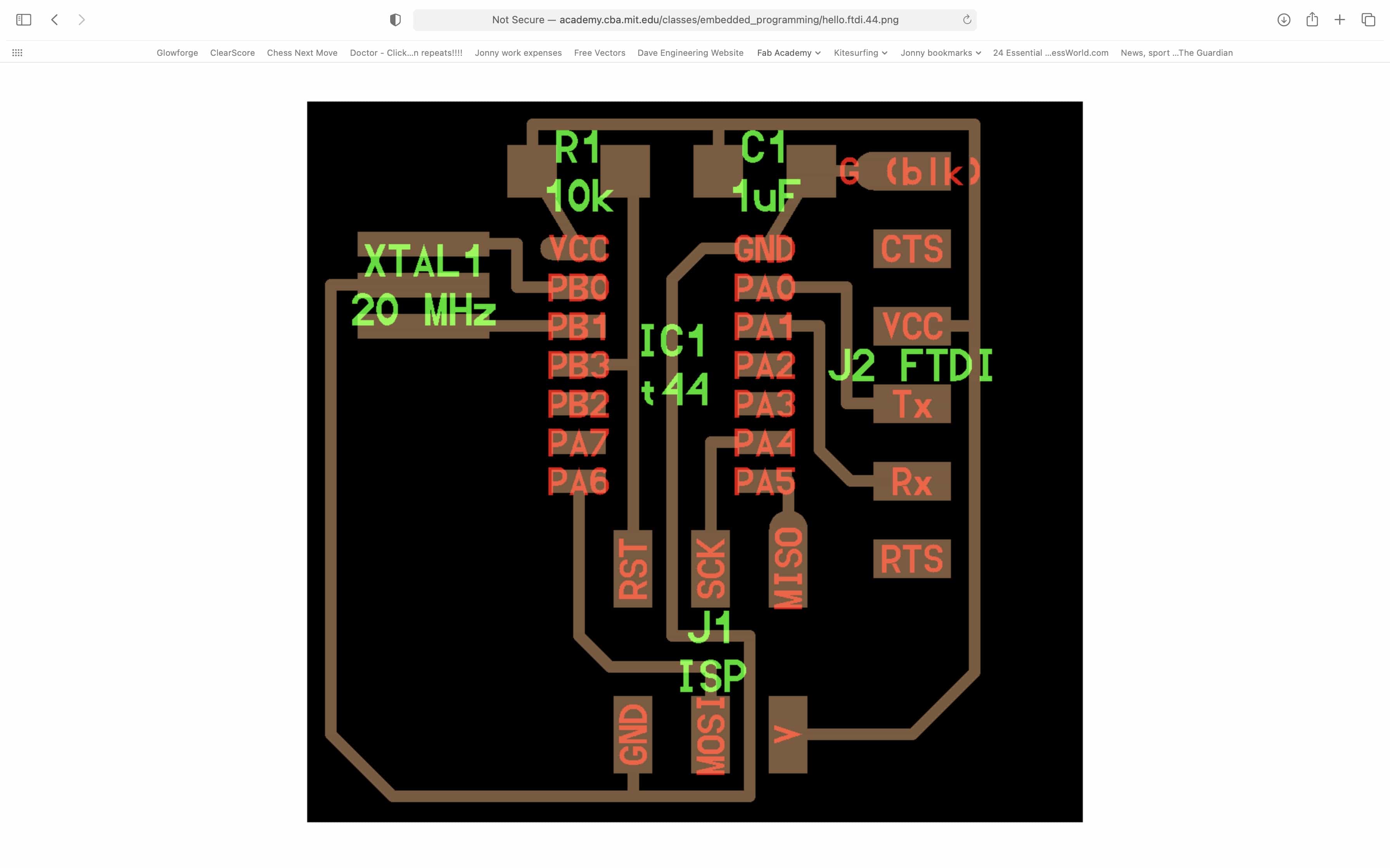
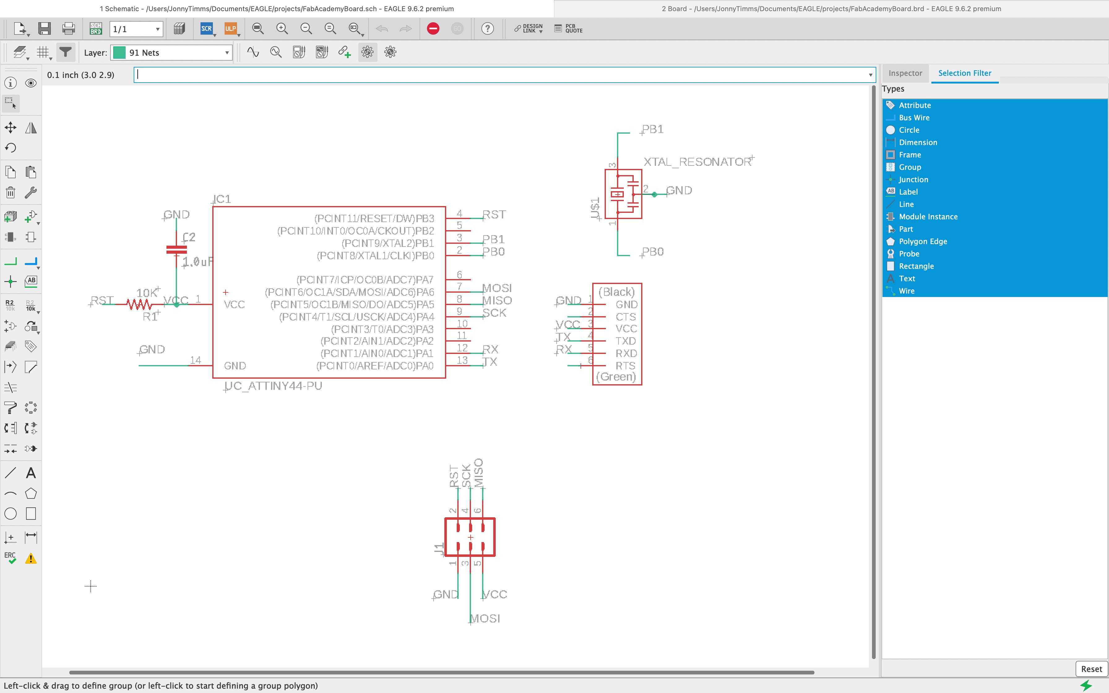
It took me way too long but I got there in the end. Here is my first schematic in Eagle, based on the circuit above:
2 - Arrange the components into a PCB design
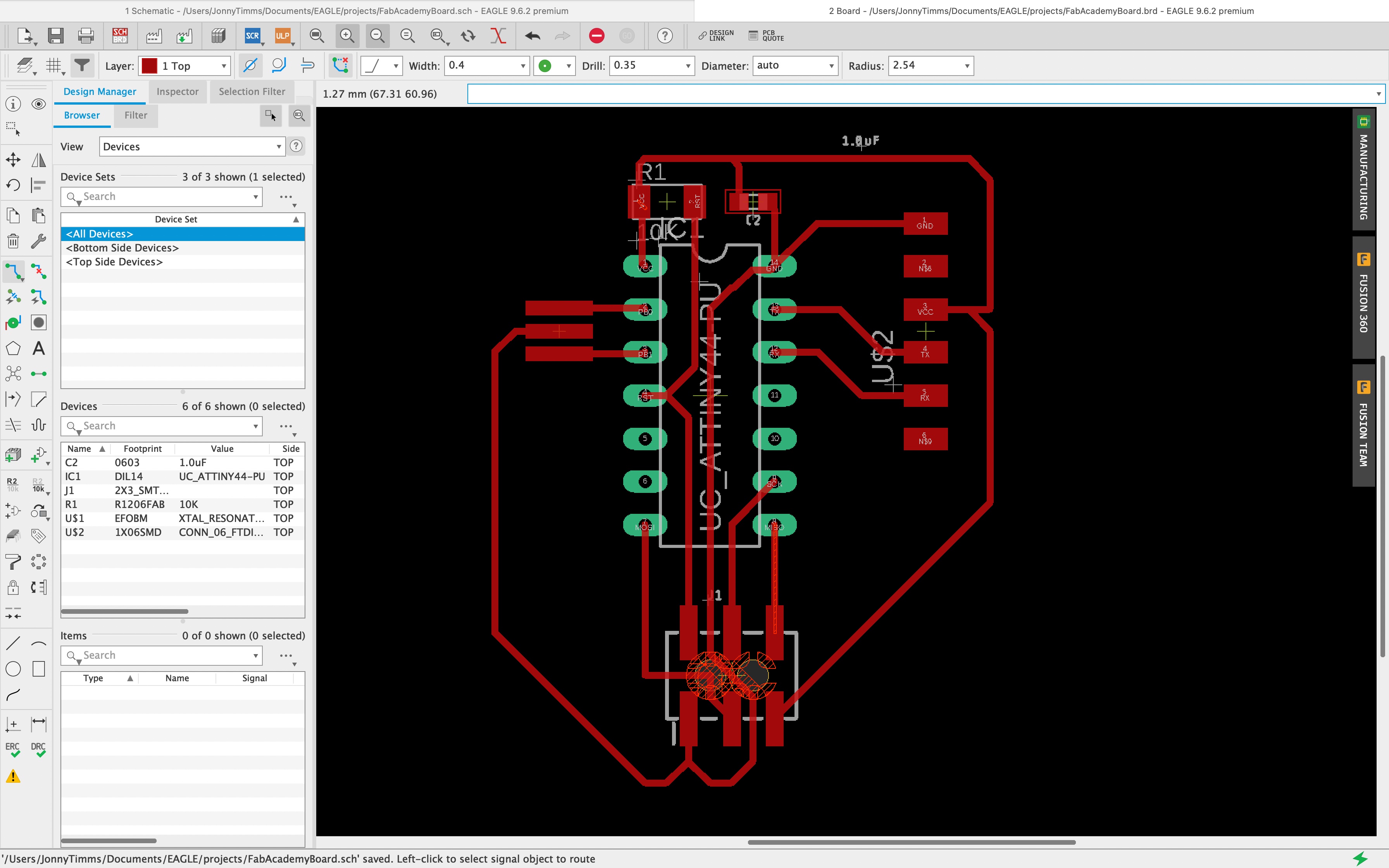
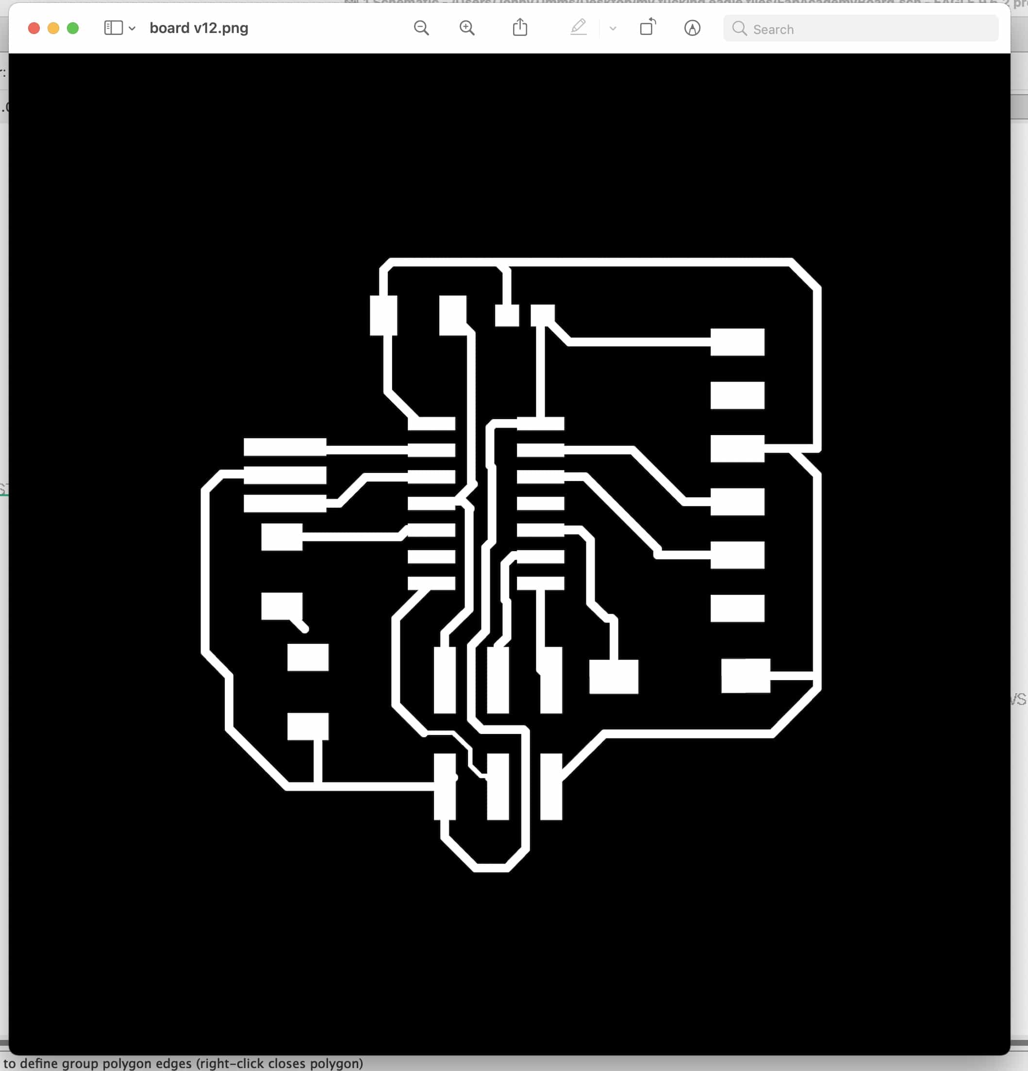
I'll need to arrange the parts in a way that allows me to make all the connections without any crossed wires. I set a clearance requirement of 0.2mm and a minimum size of 0.2mm for all the traces. I tried not to copy the PCB above but it was kind of difficult! There is an obvious design to use that best connects all the parts with all the traces clear:
3 - Export the design as a PNG
Ok so this part should be simple but it wasn't! After several mistakes I've found the workflow that works for me:
1 - Click on 'layers'
2 - De-select all layers
3 - Select the layer with your traces
4 - Click 'file/export', set resolution to 1000 and tick 'monochrome'
5 - Open the exported file in finder, set image size and reduce by half. This step is necessary due to Eagle not recognising the resolution of the macbook retina screen. (Sorry Andrew, you suggested a proper way to avoid this step but I couldn't remember what it was!)
6 - You should have 2 exported files, one for the board and one for the outline. Draw a box around the outline, crop it (CMD-K) and note down the size.
7 - Now draw a box of same dimensions around the board, making best effort to center the board within the box. Crop it and save.
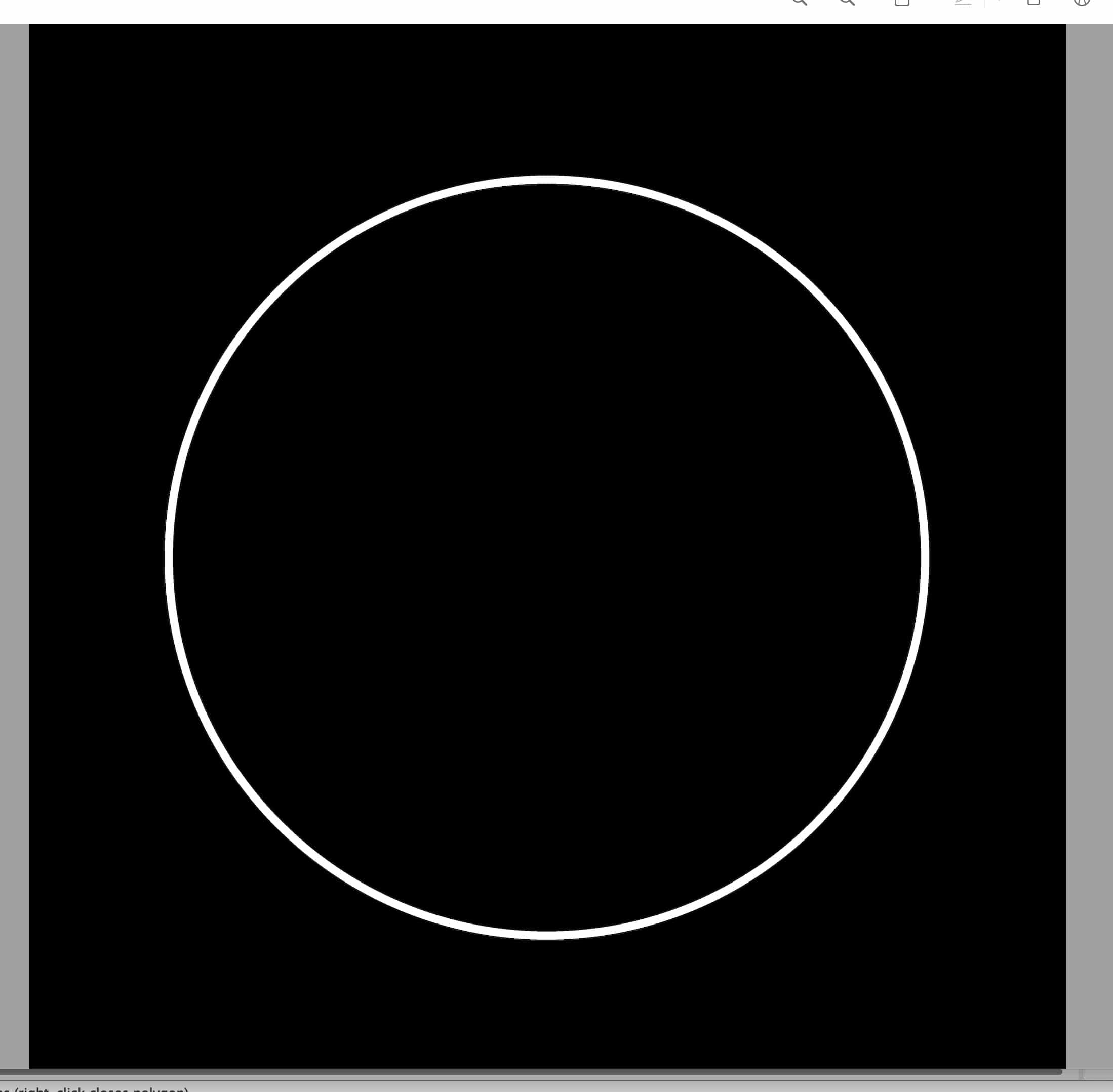
8 - Go back to outline image. Use the markup menu and select circle. Draw a circle inside the outline and extend the white circle to fill the entire outline. Save it.
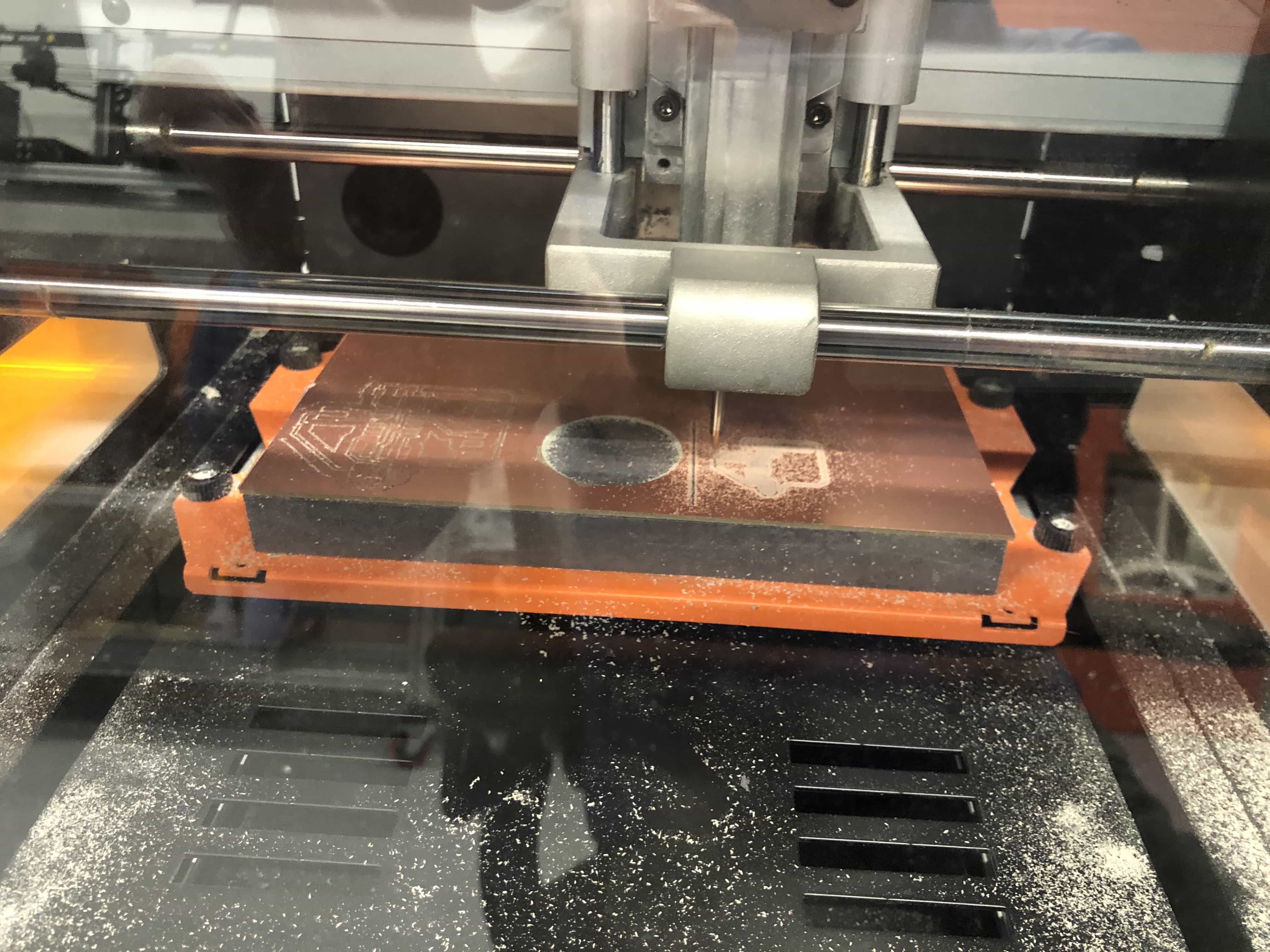
4 - Use the Roland CNC to mill the traces and outline
I covered this in detail in my week 4 assignment. I'm starting to like modsproject now. It feels a lot more simple than it did back in week 4. We'll start by setting up our 2 files and exporting as RML files:
Milling the board should have been straightforward but I ran into a series of silly problems. In no particular order, here are some of the things that happened:
1 - Set the Z axis to zero after moving it up 2mm. As a result the bit was moving just above the material, as opposed to cutting it.
2 - Didn't set the Z axis correctly. Ideally you would drop the bit into the middle of your design (you'd need to estimate this because its done before you print). I wrongly dropped the bit onto the material but away from my design. As a result the traces did not engrave correctly.
3 - Tried to cut material that was overhanging the base block. Our copper material is larger than the base block that we use. As a result there is a long thin line of material at the back which looks to be supported but it technically just floating above nothing. When I tried to cut on this material, the traces did not engrave properly.
4 - I lifted the copper material and placed it back down, but turned 180 degrees. I used the same double sided tap that was already on it. My print was doing fine but then on the 3rd pass, the bit started pushing the material off the block. That was the end of that design.
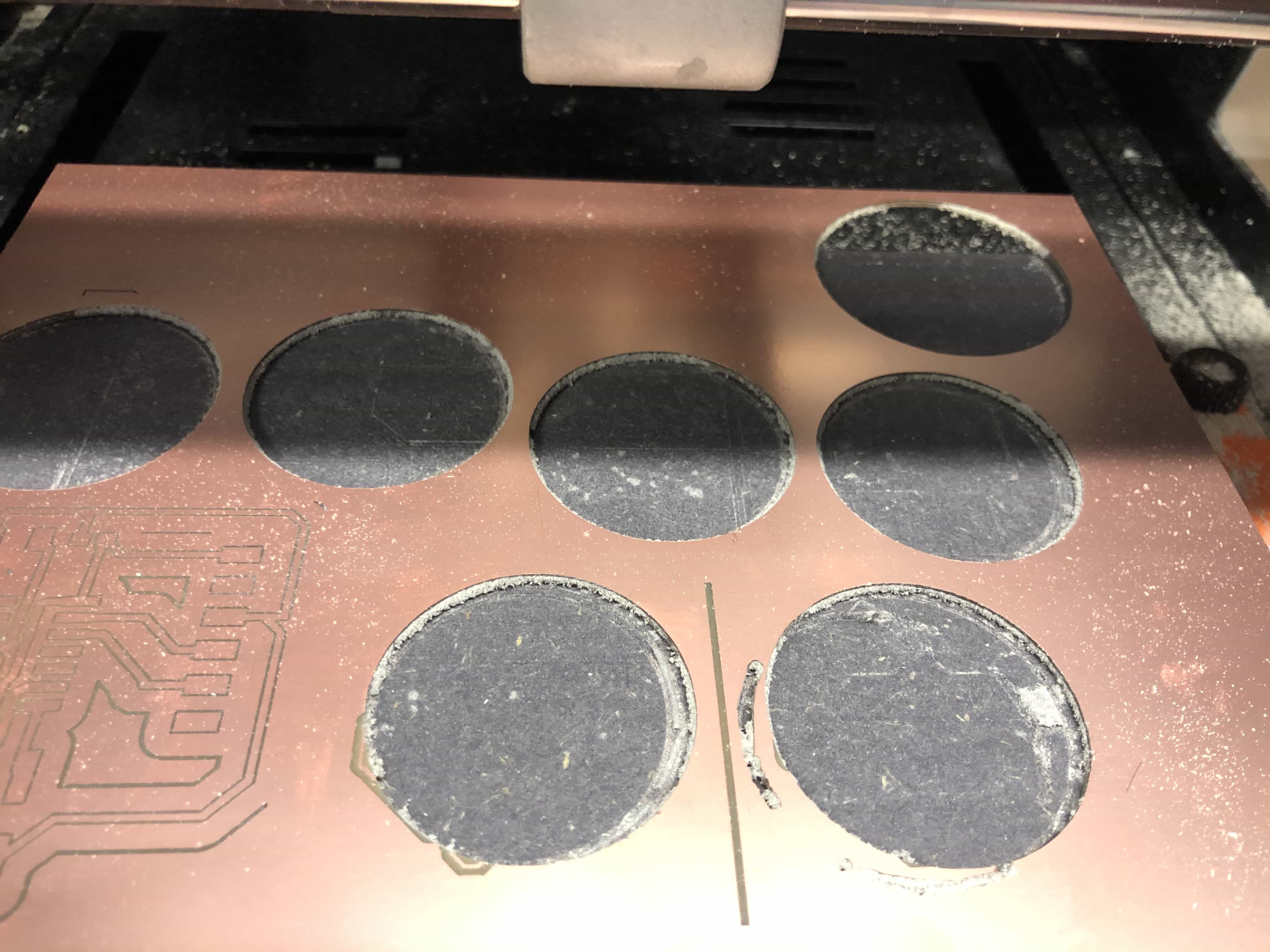
Here is the evidence for some of my failed attempts!
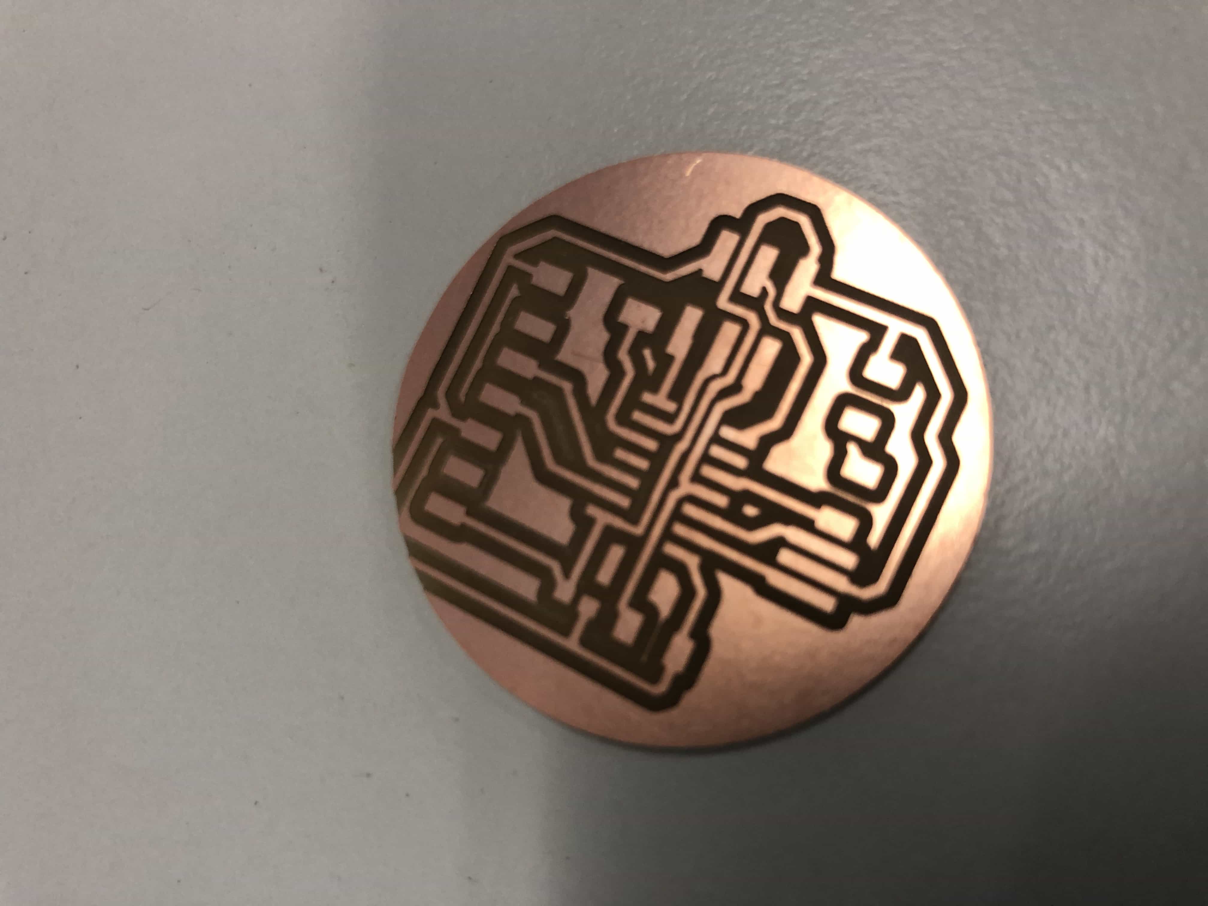
In spite of the issues above, I got there in the end! Here is one of my printed boards:
5 - Solder on all the components
I've covered soldering in detail in my week 4 assignment. This should have been straightforward but I still had a couple of issues:
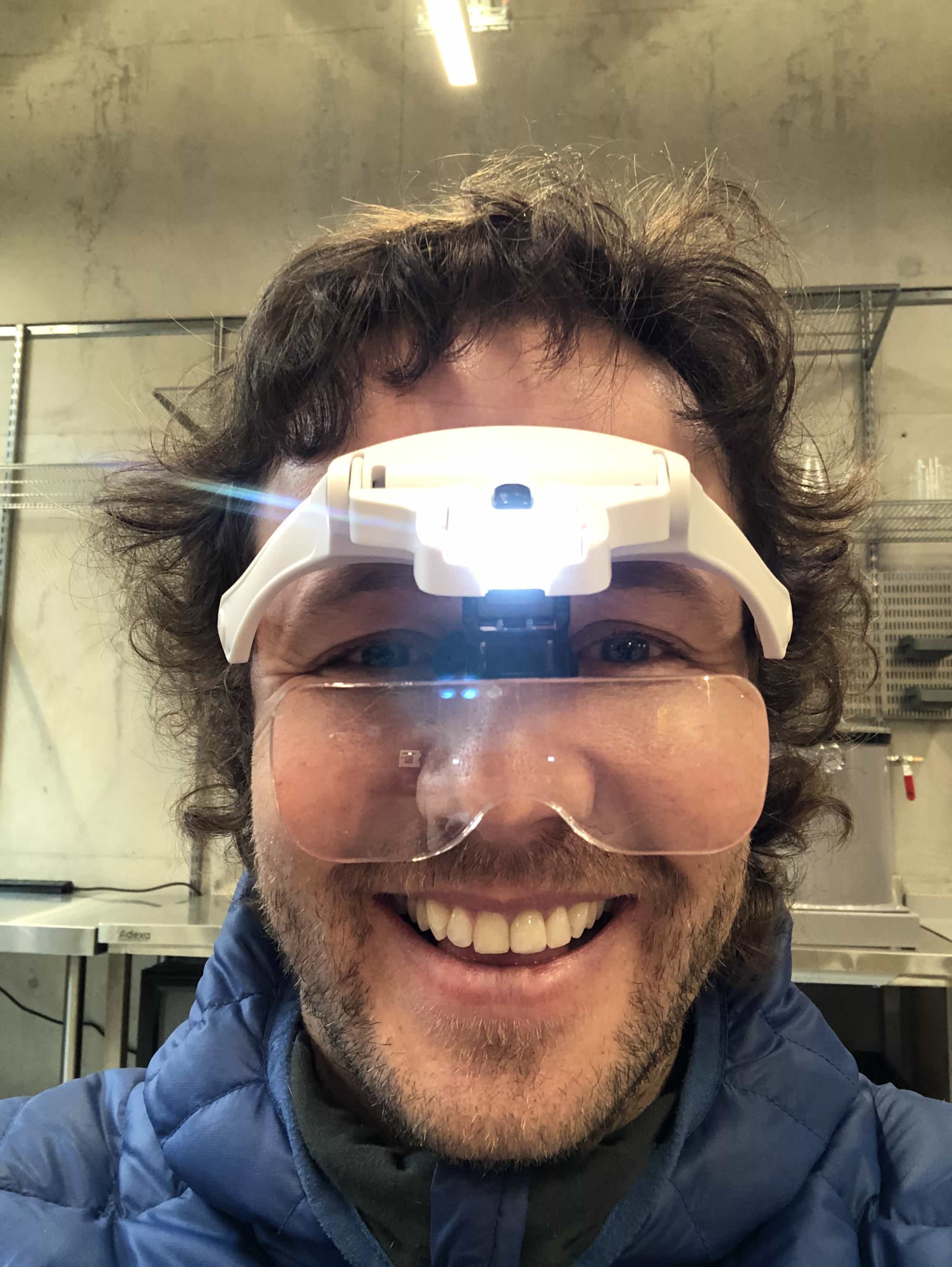
1 - Yet again I forgot that the main chip is directional. I find it so hard to read the text and maybe this discourages me from remembering to check! Either way I remembered that i had bought some magnifying glasses some time ago. I dug them out and they are brilliant, they make so much difference for intricate soldering:
2 - After soldering the chip the wrong way round, I attempted to de-solder and remove. Unfortunately i struggle to get all the solder completely off and when I pulled the chip, it removed some of the traces. The board needed to be made again.
Eventually I managed to solder a board correctly:
6 - Programme the board using our ISP programmer from week 4
This should be the fun part and again, in theory it should be straightforward! For me it has been anything but simple. My ISP programmer is appearing intermittently and my ATTiny44 board is unable to be found by Arduino.
Katie had similar issues and was finding it stressful. Then suddenly it all worked and she was super happy! I'm very happy for her and my moment will come soon...
It seems the reason for the issue is that the ISP programmer has issues with connectivity on the USP port. Although we added some solder to these pads, its hard to get them of equal height. Its now my plan to re-make this board but using a mini USB connector so that i can connect it to my macbook using a cable. I'm going to go ahead and do this but it will not be in time for this week's lecture. I'm hoping to complete this on Wednesday evening.
2nd attempt with an ESP32 chip
Schematic design
After spending some time learning Eagle, I've concluded that I find 'Easy Eda' a lot easier to use. In particular the user-contributed components are just so incredibly helpful. Its often the case that the professional libraries seem to miss the actual thing I need. Its quite likely I'm just searching for the wrong term, but even so, thats still an advantage for the user-contributed parts. It feels like people use more layman terms to describe a part and that seems to be a better match for the type of things I'm typing when I search for components.
So with that in mind, I got to work building a new schematic in Easy Eda. I've noticed people putting rectangular boxes around groups of parts and I've decided to do the same as I love how clean and tidy it makes things look.
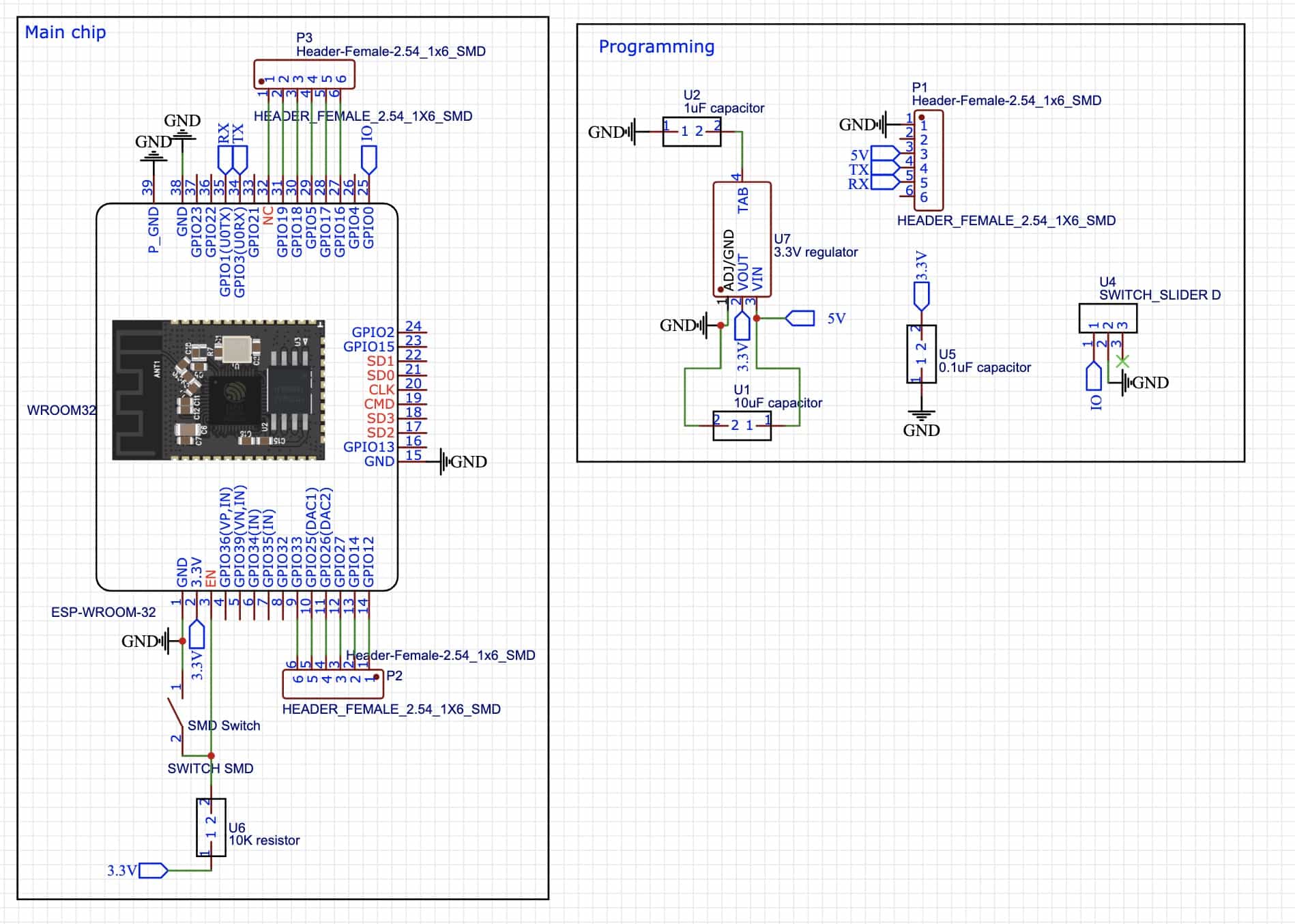
The schematic above is based on Neil's ESP32 board. It has the essential buttons on the EN and IO pins. These switches allow you to pull each pin to ground which is required for uploading your sketch. The EN pin also has a pull-up resistor to the 3.3V. I'm unsure why the IO pin does not require this but if its good enough for Neil, I'm happy.
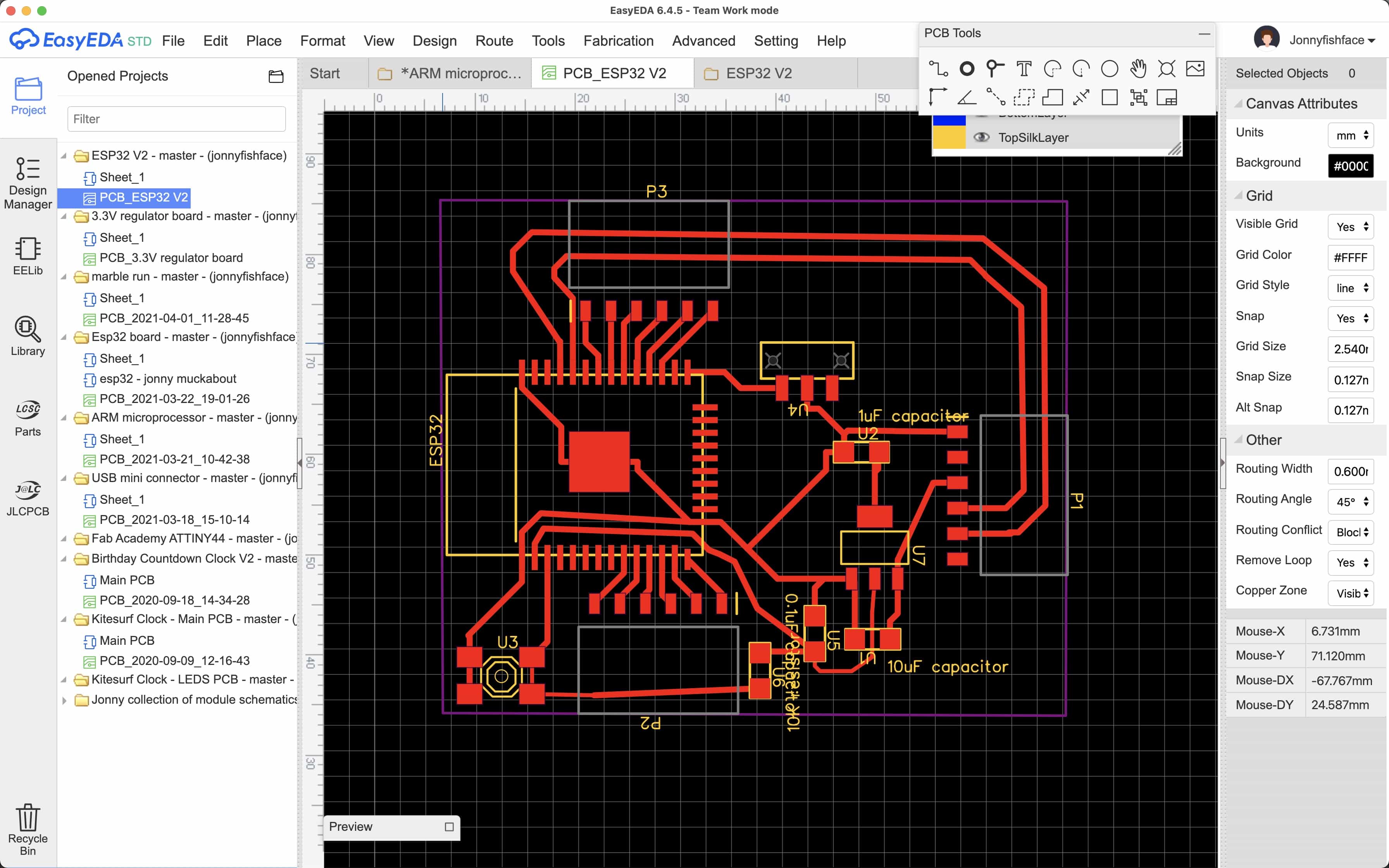
PCB design
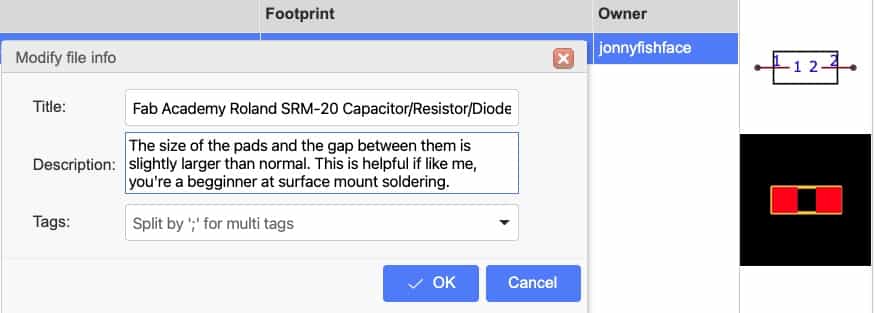
I've decided to do something a little different this time. One of the issues I've had with previous boards is that the surface mount pads for the resistors, capacitors and leds seem to be a little small. Technically they are sufficiently sized but it would just be easier to solder if they were a little bigger. The gap between the pads has also been a little too small which has caused a problem when I'm trying to use the component to create a bridge over a track. Our Roland SRM-20 is unable to cut the gap between pads and tracks. I've solved this issue by using a knife to cut the copper but I'd rather avoid this.
Making the pads larger is perhaps not a scalable solution. No doubt there would come a point where a lack of space on the board made the larger footprint a poor choice. While my surface mount soldering is still a little amateur, it feels like a smart choice to use larger pads on boards that are simple and with ample wriggle room.
So with that in mind I've followed an excellent youtube tutorial for making your own component:
 https://www.youtube.com/watch?v=utBQqcuOt9U&feature=emb_logo
And here it is! My first custom component in Easy Eda:
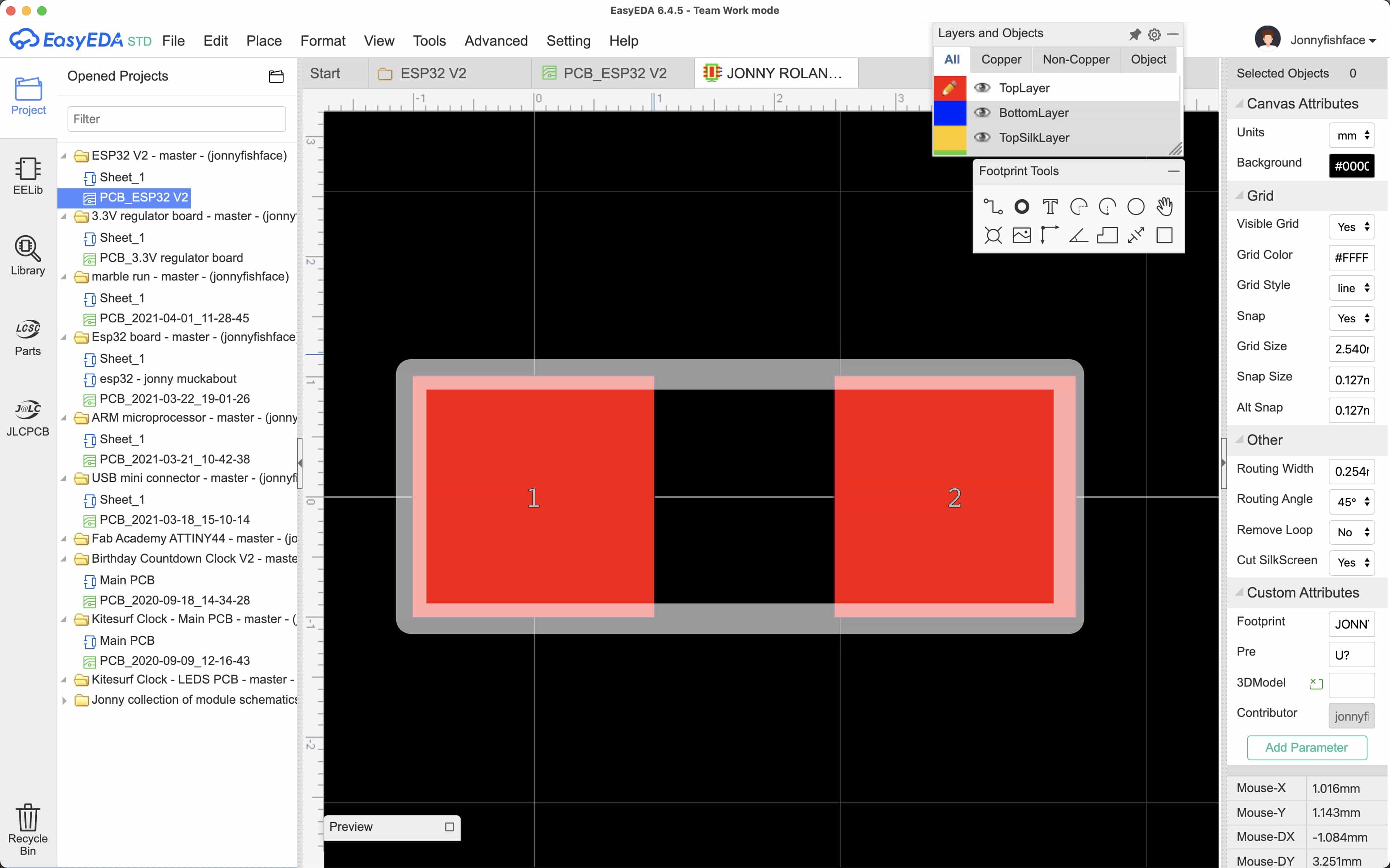
I've given the part a meaningful name and description. This helps me to remember what it is and why you might use it. Furthermore, other Fab Academy students may find this part if they search for the name of our course. The description should help them assess whether this part is suitable for their needs. Here is the date for the part listed on the Easy Eda database:
Managing favourites and custom parts
There is an annoying quirk in Easy Eda which means you can't add a part from your schematic into your favourites. You can only add a favourite when you're looking at the part in the library. As a result I've never added any parts into my favourites.
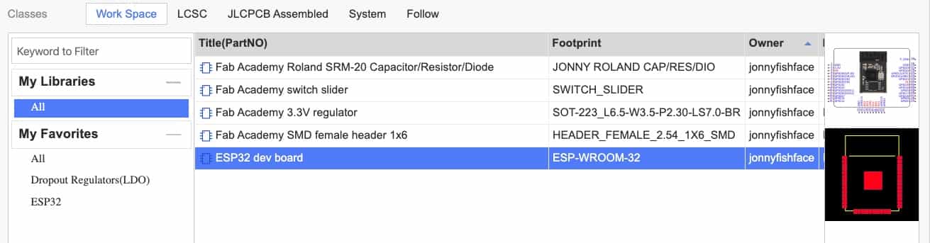
I've finally done what I've meant to do for a long time and I've gone back into the libraries, found the parts I've successfully used and added them to my favourites.
I wanted to give the parts a custom name but this was not possible unless I cloned the part and created my own version. So I've done exactly that. I now have 5 custom parts but I expect this to grow slowly through the rest of the course. I've included 'Fab Academy' in the part name for any part we hold in stock in our lab. This way I know the part I'm using has the exact footprint of the version we have in stock.
My custom library now looks like this:
Autorouter
I've intentionally avoided using this so far in the course. It confuses me slightly because I've now watched 2 separate tutorials on circuit design, both of which had someone using the autorouter yet asking the viewers not to hate them for doing so!
I chose to use it for this board and I tidied up the bits that they missed (2 tracks) and made a mess of (a few other little bits). It felt like a good compromise to use the autorouter with the intention to use the results as your startpoint to some manual arrangement.
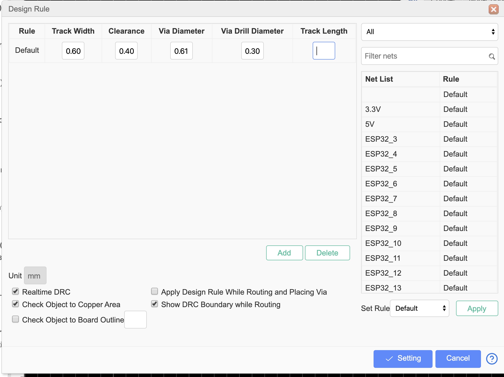
I used larger tracks this time (0.6mm) and slightly larger spacing (0.4mm) to take account of our 0.4mm mill bit on the Roland SRM-20. Here you can see the design rules for my board:
Now here below is the complete PCB using all of my now 'custom' and 'favourite' parts.
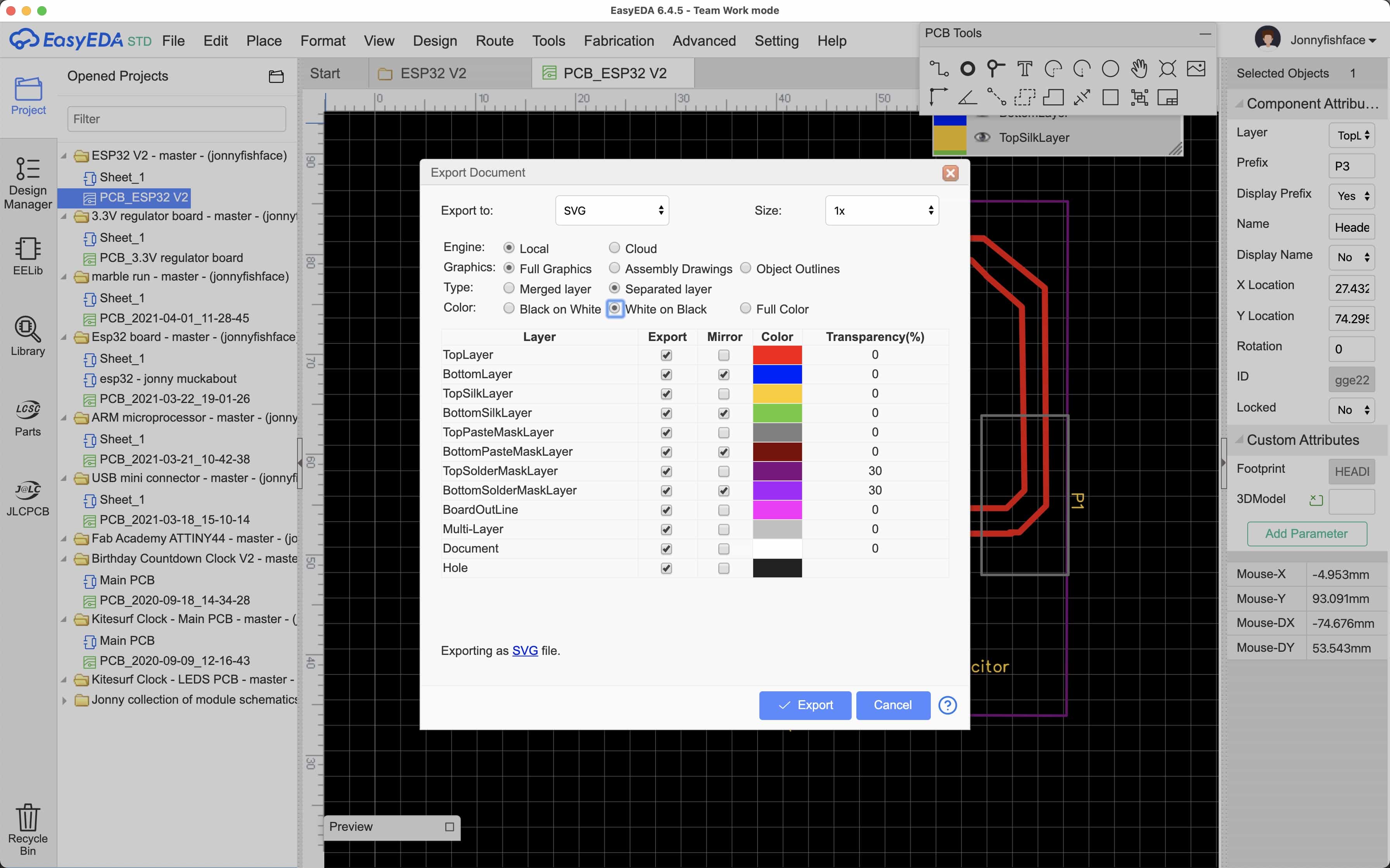
Exporting the file ready for Roland SRM-20
After a lot of trial and error, I'm confident that the following workflow is the smartest way to do this:
1 - Click export and use the following settings:
- Export to - SVG
- Size - 1X
- Engine - Local
- Graphics - Full Graphics
- Type - Separated Layer
- Colour: White on Black
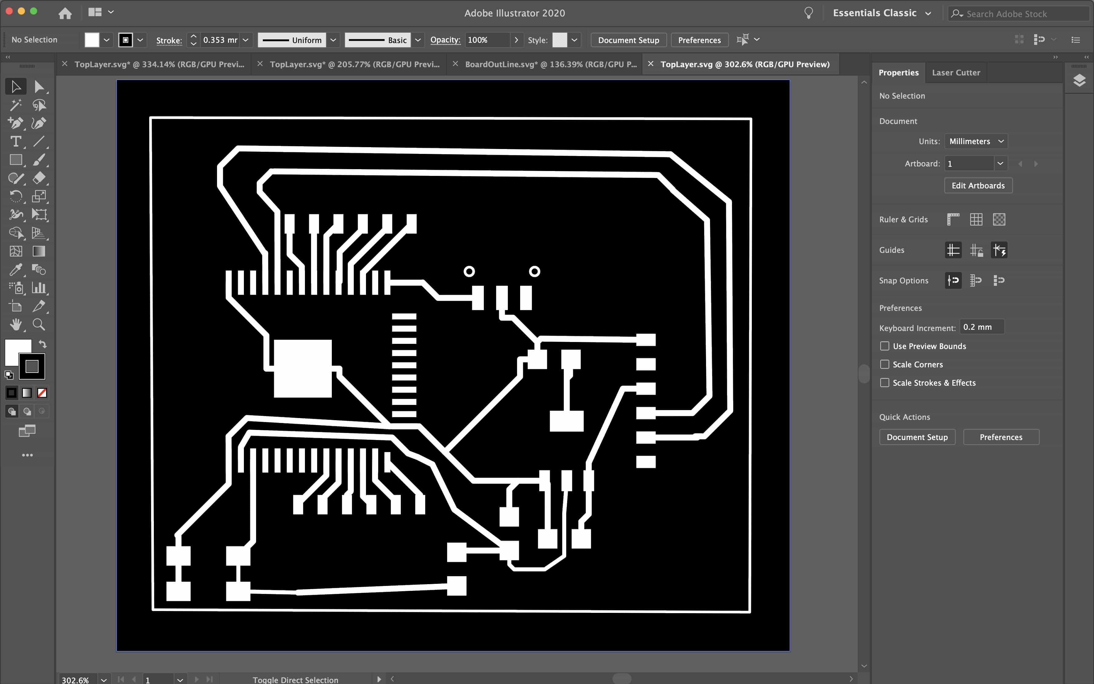
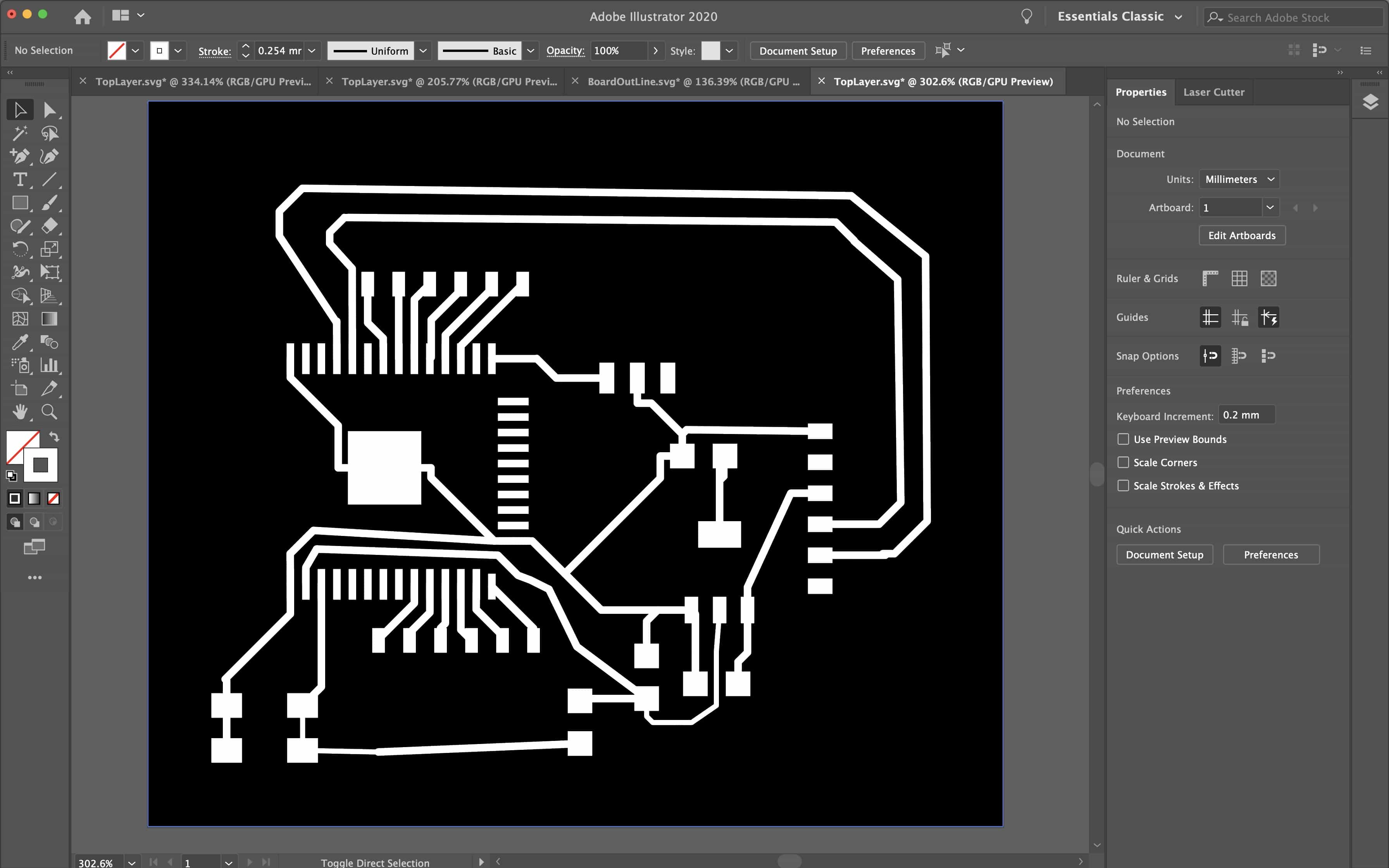
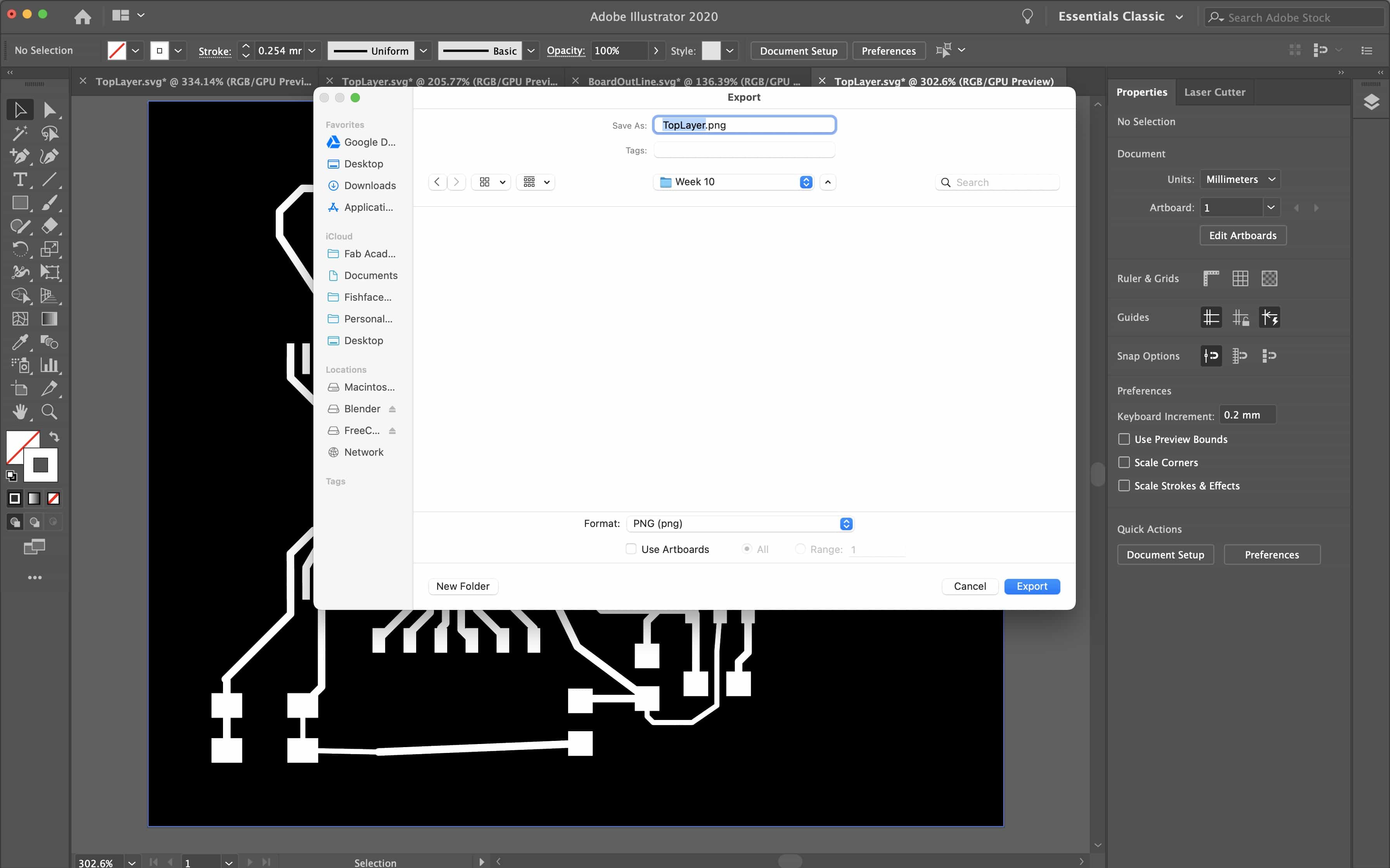
2 - Open the SVG file in Illustrator and make any edits. You'll see on the screenshots below that I needed to remove some small circles on the traces file and to fill the white border on the outline file:


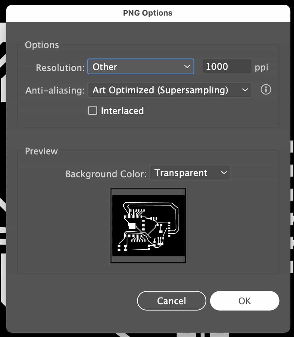
3 - Export from illustrator and select PNG as the file type. Make sure to set the resolution to 1000 PPI.
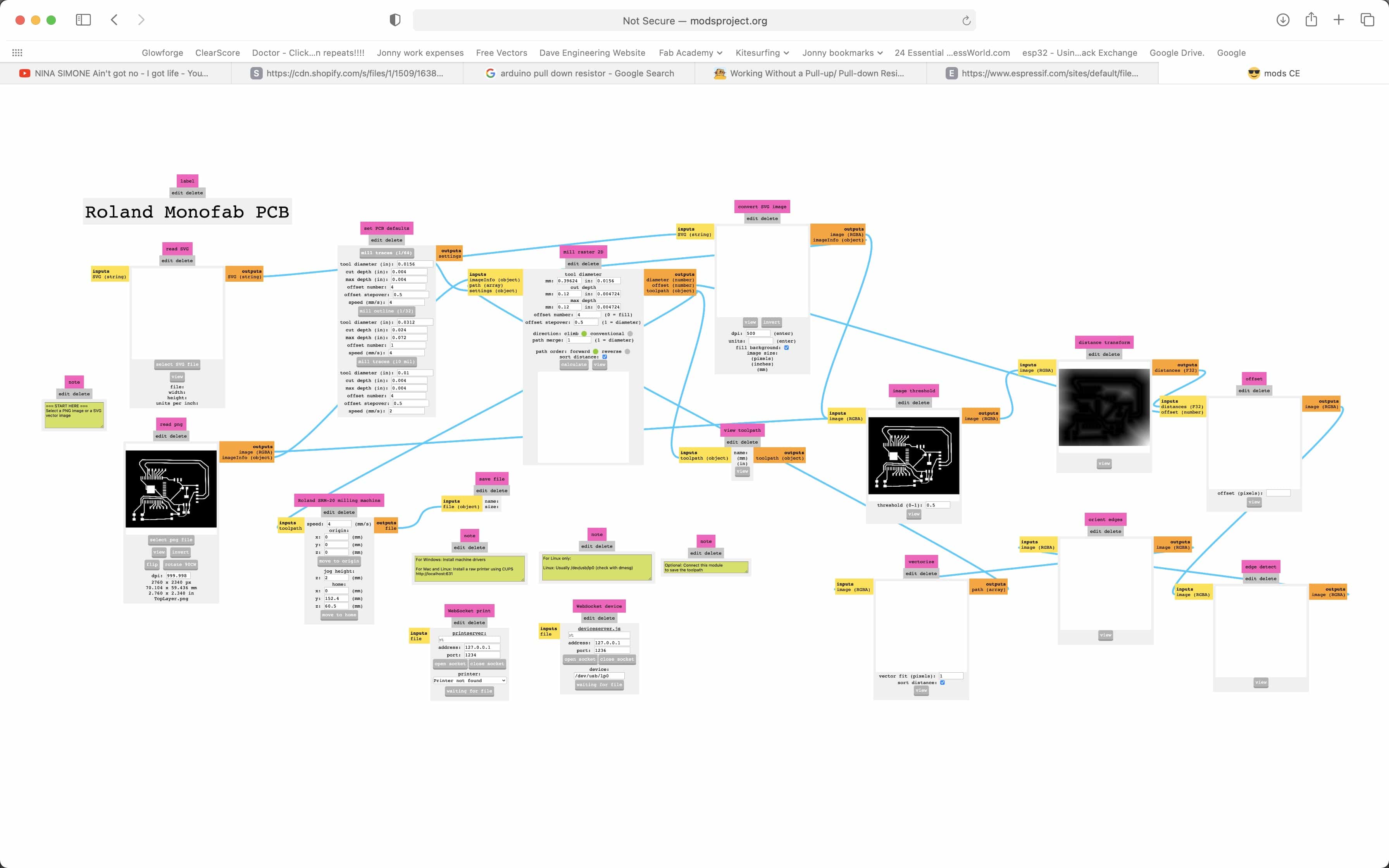
4 - Open modsproject and add your SVG file. The rest of the workflow in Mods is same as aboe where we had used a PNG file:
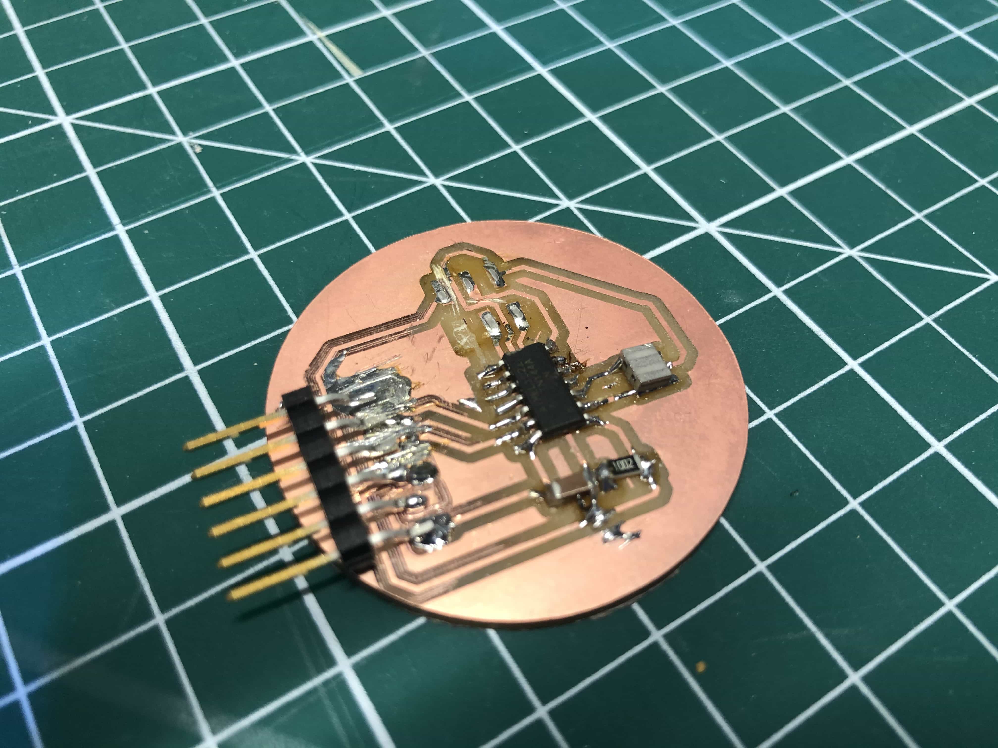
My new ESP32 board
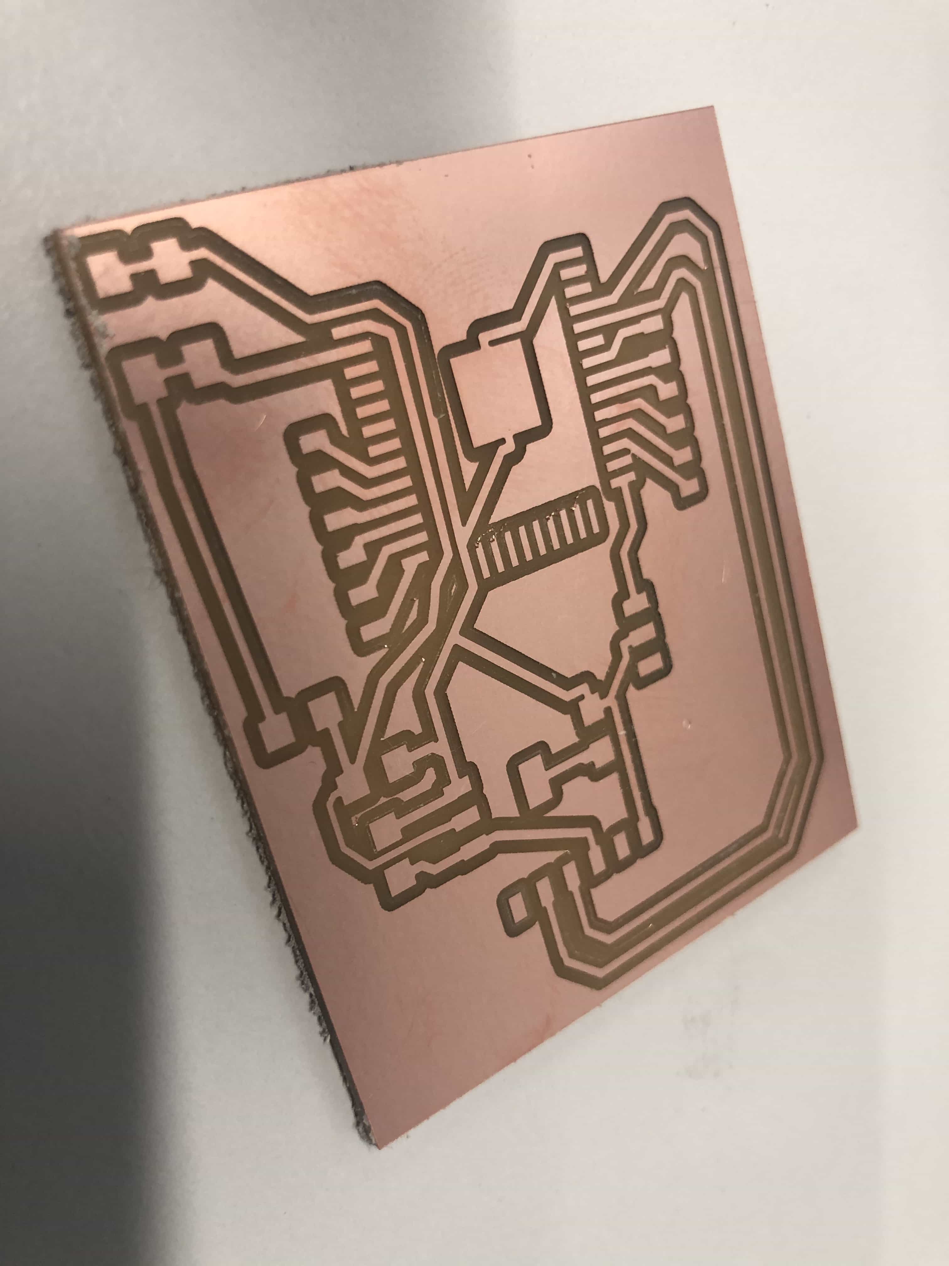
My new board has come out beautifully from the Roland SRM-20. (Sorry but I forgot to take photos this time). My solder work is slowly improving and it was a lot easier to solder now that I'm using the larger pads for the components.
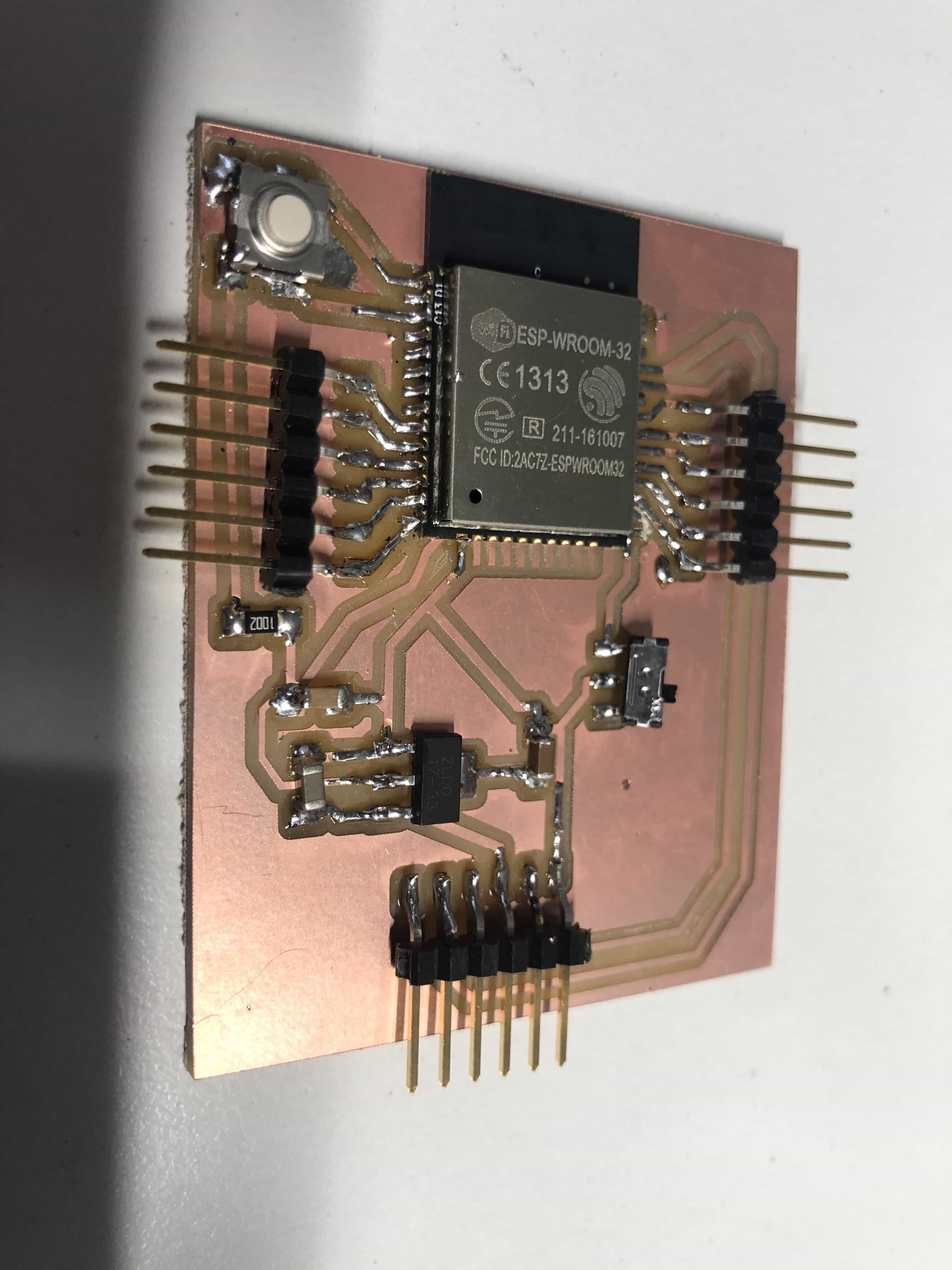
Copper around the receiver
Normally you should remove the copper around the receiver. The copper on my current board could interfere with the wifi or bluetooth signals. If I made this board again, I would remove this copper. Given that I will not use bluetooth or wifi, there is no need to make my board again on this occasion.
Adding inputs and outputs
I'm adding the following during Week 19. Below you can see my board connected to my stepper motor shield. The code is successfully moving a skateboard around my model and the INO file is available for download below.
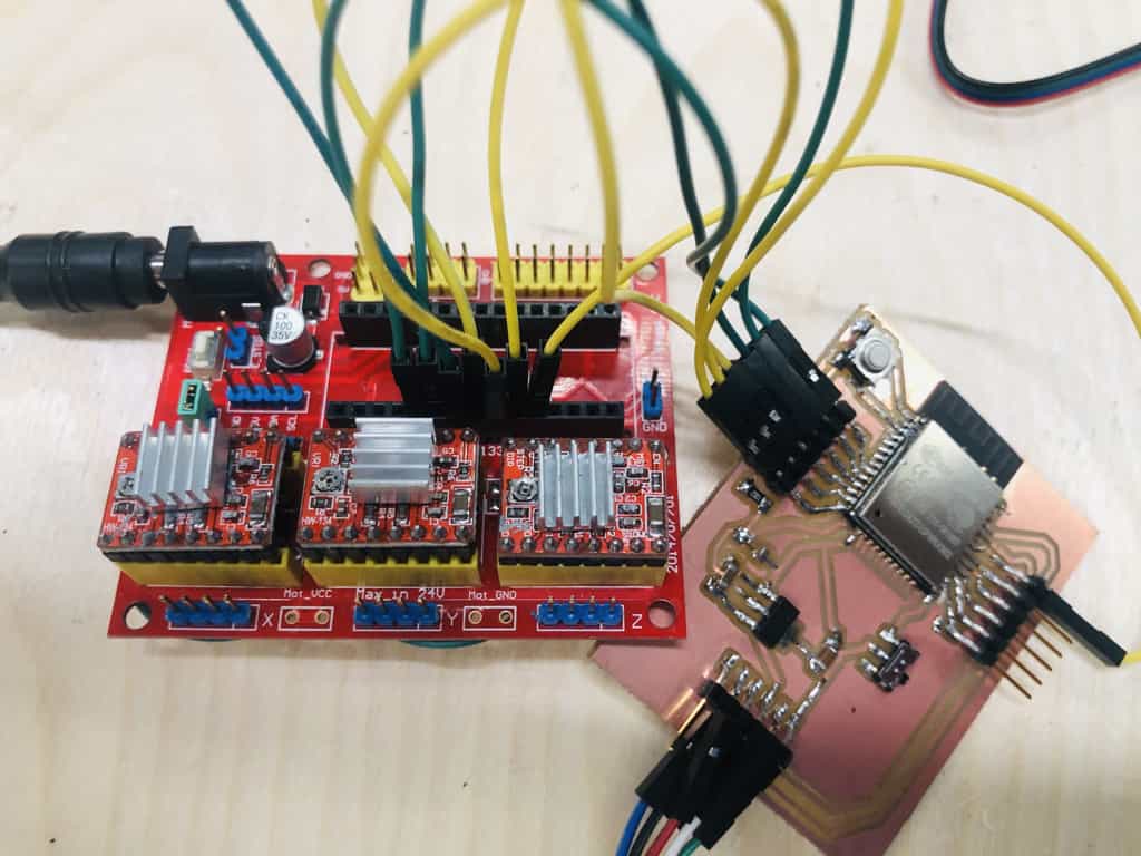
This video shows successful movement of the skatboard, powered by my esp32 board:
Group Assignment link
Files for download
Back to homepage: