Week6
Electronic design
Go to:Group assignment Individual assignment
Group assignment
Use the test equipment in your lab to observe the operation of a microcontroller circuit board (in minimum, check operating voltage on the board with multimeter or voltmeter and use oscilloscope to check noise of operating voltage and interpret a data signal)
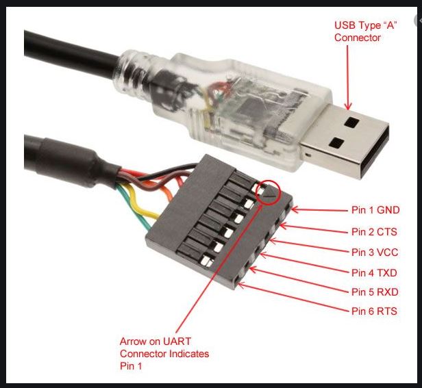
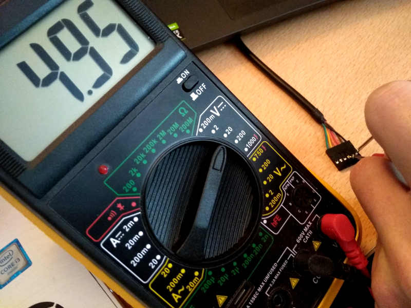
So far I have been using the multimeter to test continuity in my soldering and the polarity of some components (example can be seen in week4). I also used it to figure out the resistor value for the LED I am adding. I mesured the power supply voltage from the FTDI cable I will be using, it will help calculate the value later on.
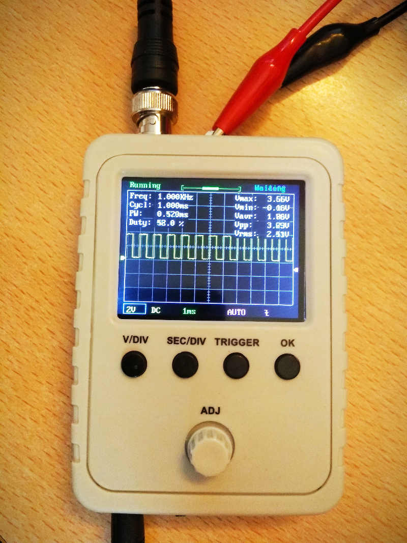
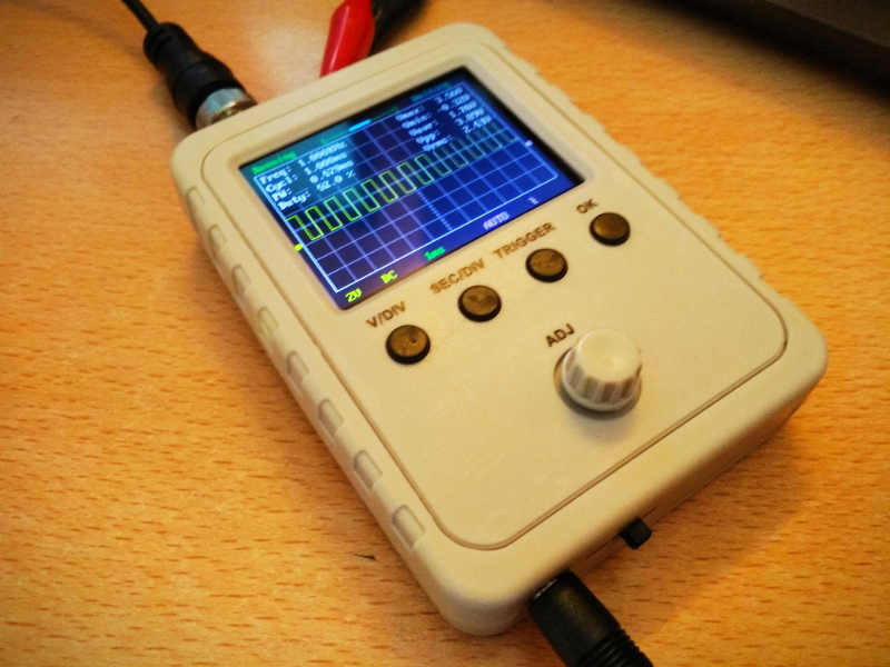
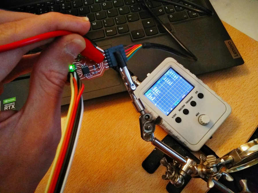
This is the small osciloscope I will be using, here I am just testing it functionality.
Here I am probing the voltage going in the board, I can see the voltage but I have no clue on how to interpret the data signal yet.
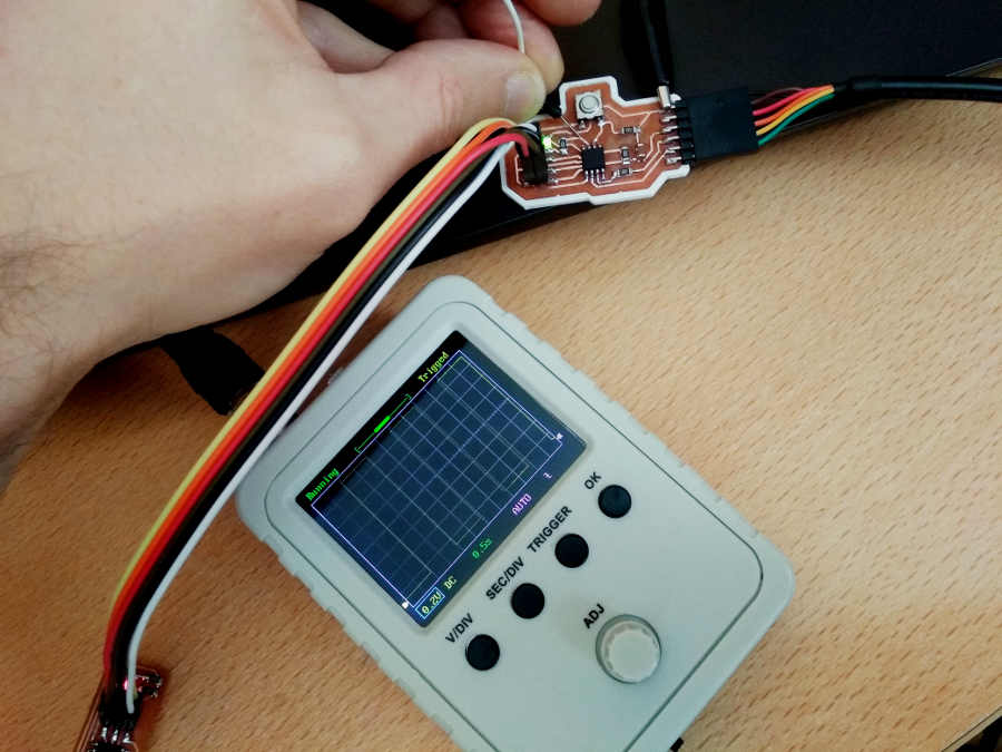
Conecting to the GND and pin PB4 (in my case the pin for the LED) I can see the signal being sent.
Go to:Group assignment Individual assignment
Individual assignment
Redraw one of the echo hello-world boards or something equivalent, add (at least) a button and LED (with current-limiting resistor) or equivalent input and output, check the design rules, make it, test it.
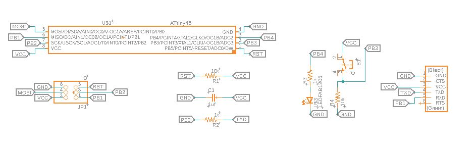
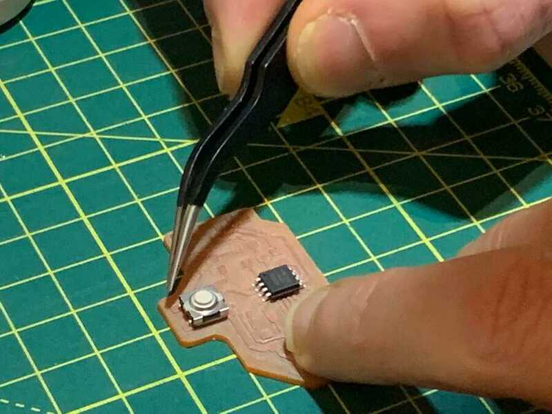
I started in fusion (Electronic design/eagle section) and looked for the components. In my case I am making the “hello ftdi 45” with:- X4 resistors, 2 that were already on the board (pin PB2-1k and RST-10k), one for the pull down 10k and another one for the LED 1k.- x1 LED (green)- x1 Capacitor-1uf- x1 Push button- Attiny45- x1 2X6 pin connector- X1 FTDI smd connector pins
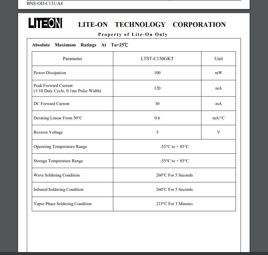
I found the data sheet of the LED here to find the forward voltage and current.
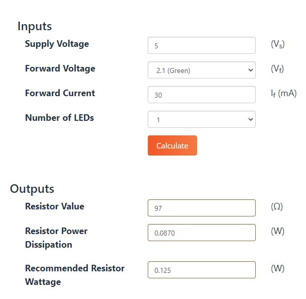
Using ohm´s law we can determine the resistor value and I find a nice calculator here I used a 1k resistor in the end.
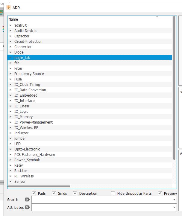
I already found a useful Component library 2 weeks ago (Here) but I went and downloaded this one as well.
Here is my attempt from 2 weeks ago
Download (to a safe place) and browse the computer from the library manager (in use) and select the downloaded file to be used in this project (it appears in the list once loaded).
I started inserting the components needed on the canvas following this example along with the LED, button and resistors to include in the board.
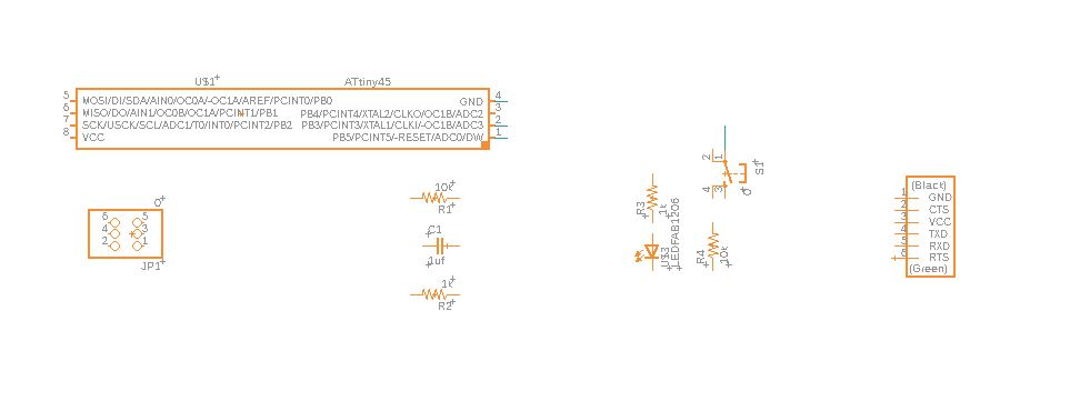
As I understand, we use the pull up/down configuration to “reset” the status of the pin used, in my case I have a pull down or a "reset" to status “0”, putting the resistor to GND but I could also use this type of configuration to create a pull up resistor or a reset to status “1”, putting the resistor to the voltage if needed…
I went and got the data sheets for the attiny45 on the seller´s website, here.
I found the pin configuration and a block diagram.
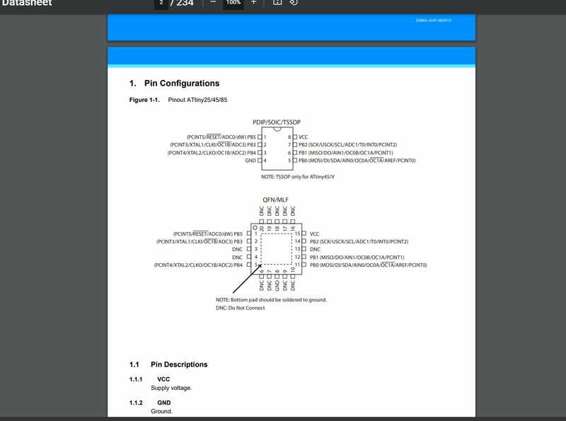
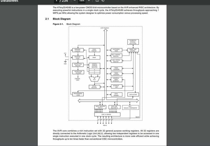
Drawings and a lot of other information that I do not understand.
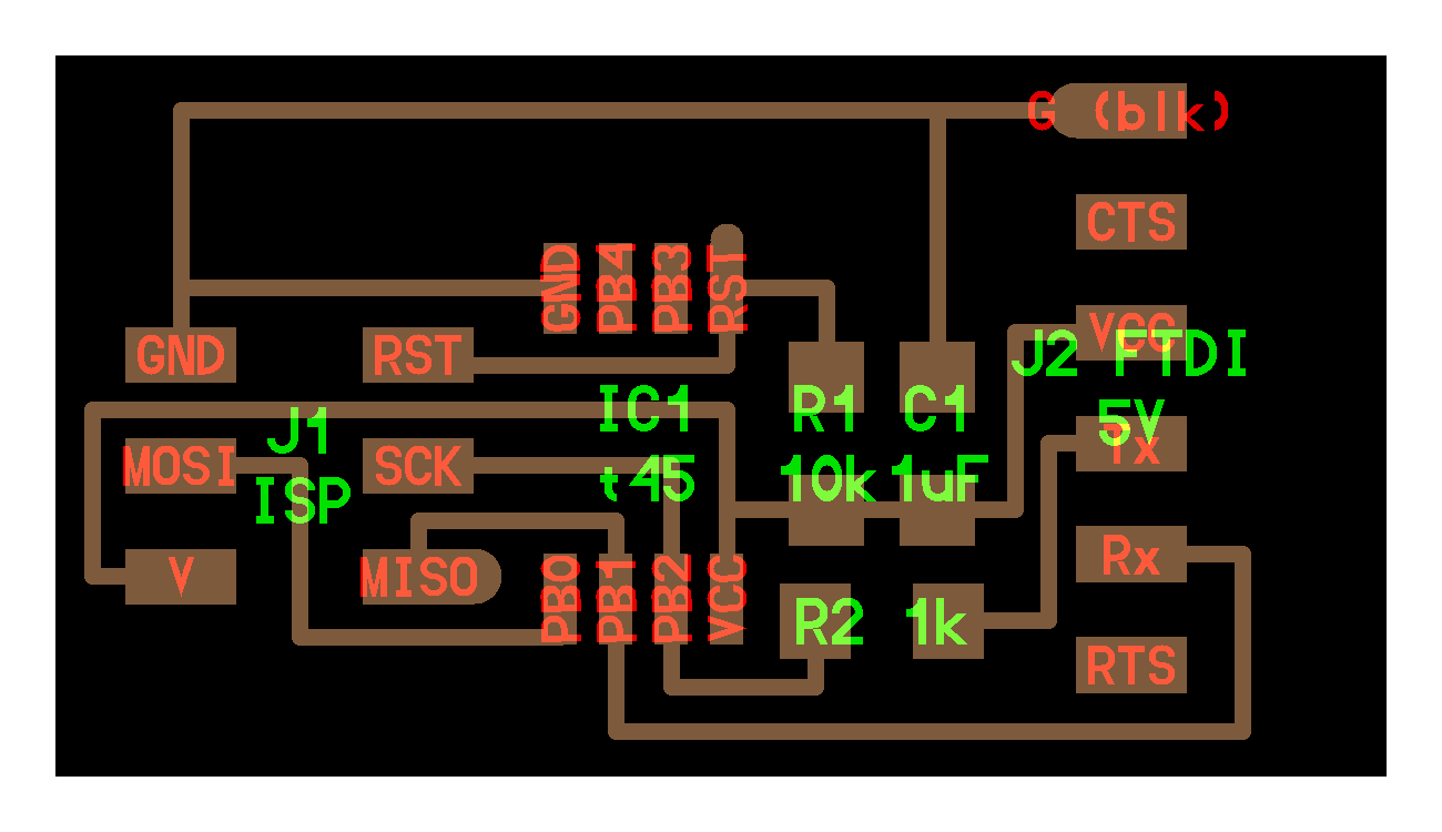
Here is how I connected my first schematic
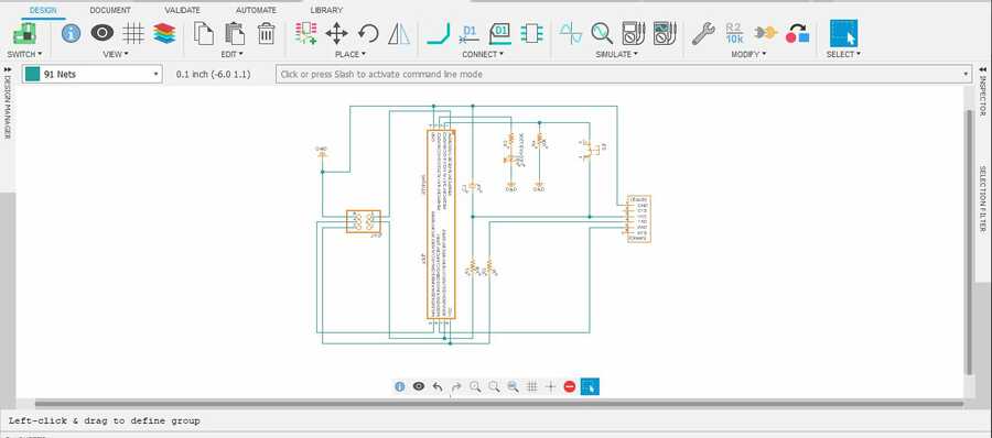
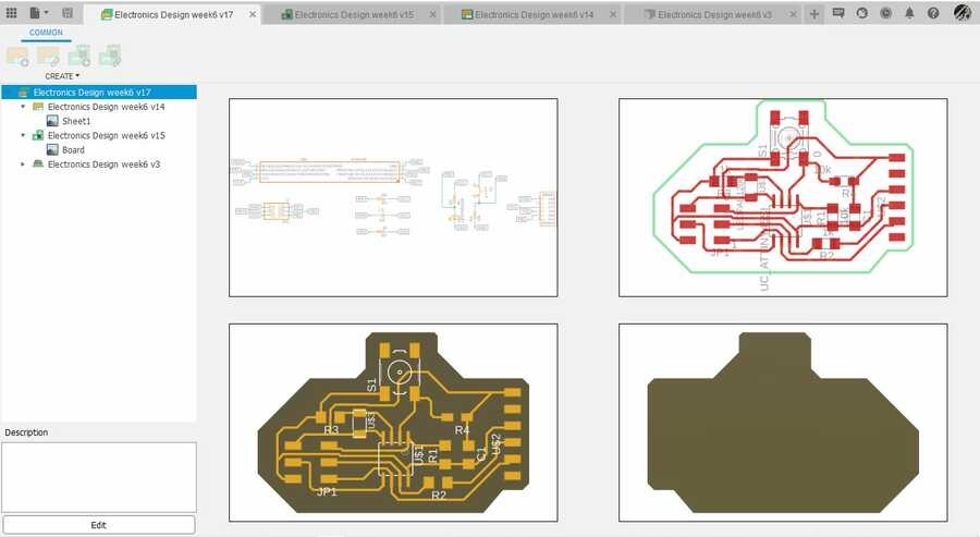
I am now moving to the layout or the pcb design section. There I can lay out the component, taking care of their orientation and location to facilitate the routing (if possible)
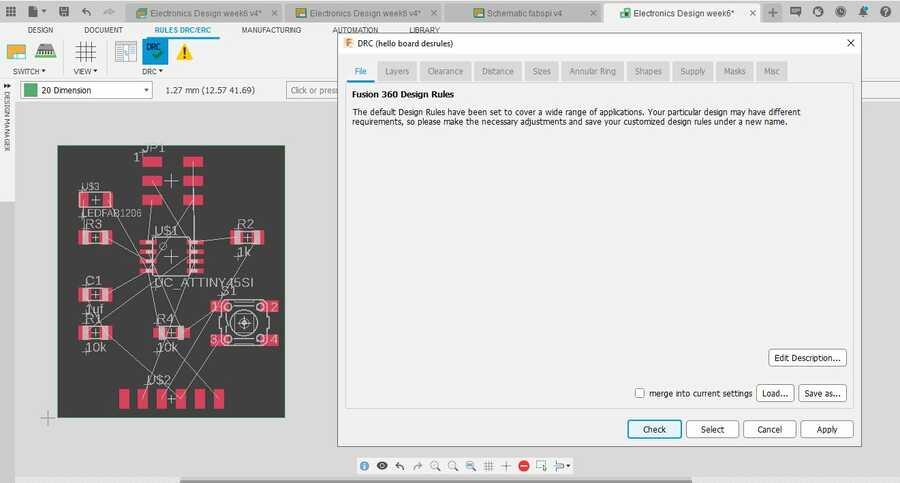
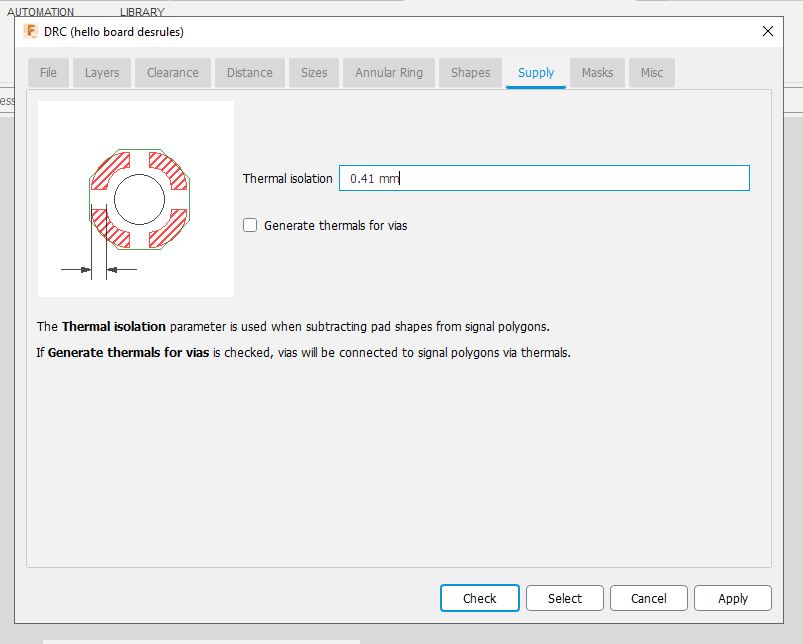
I first need to set the design rules or DRC, these can be saved and reused, here is the ones I created. There I will set:- Clearance
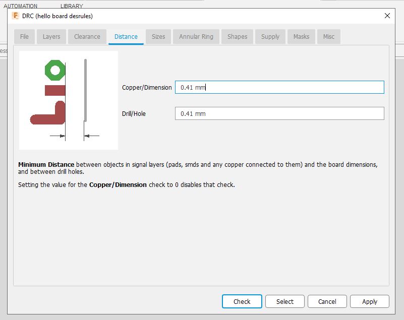
- The distance
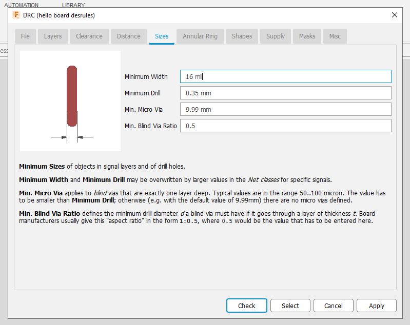
- Size
- I also changed the supply even if I am not using vias or making a ground plane.
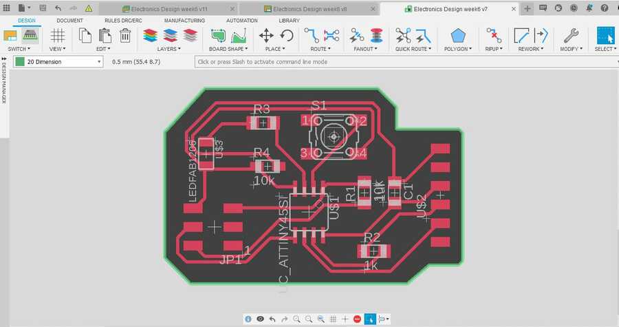
Once set I can proceed with the shape of the board using the tools provided, trying to leave enough space for the routing…
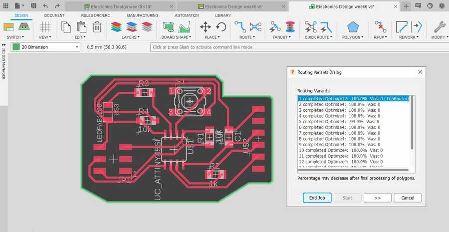
The auto routing keeps failling but after modifying the shape of the board, I was able to finally get the auto routing to produce 100% option choices for the layout of the components.
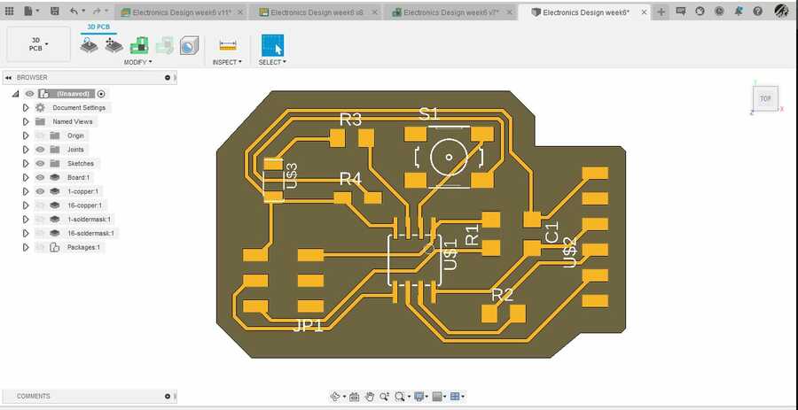
Unfortunately it look like the assets are missing and the components and their volumes are not showing…
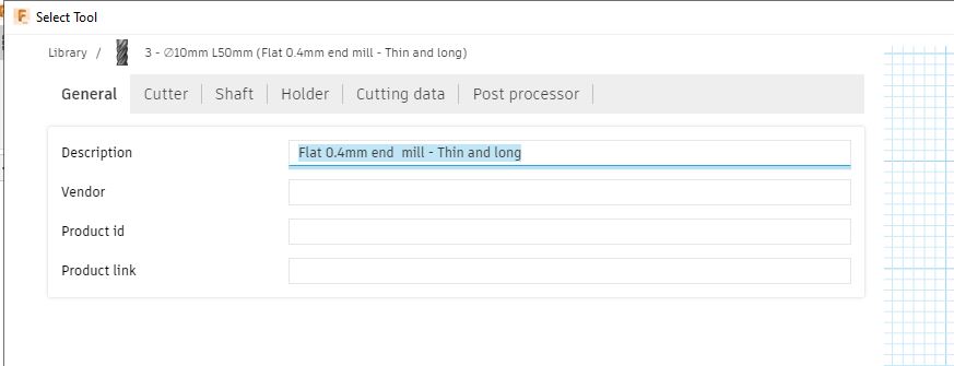
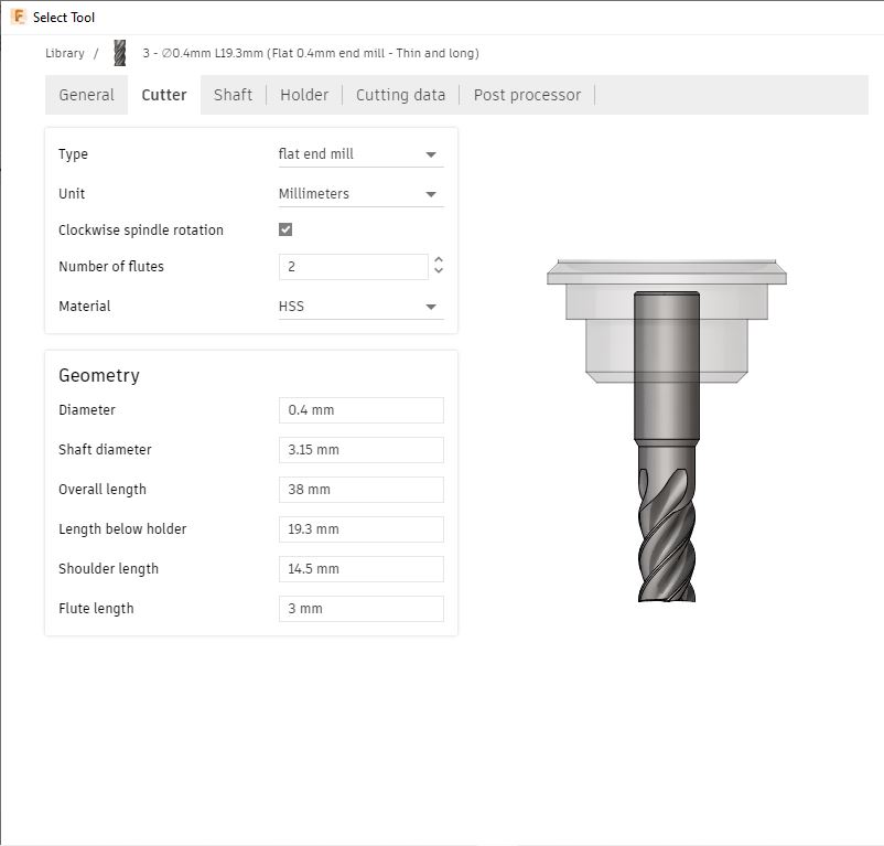
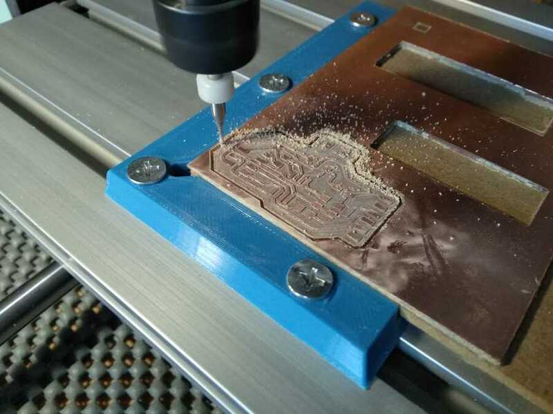
I am now going into the manufacturing section and added the tool I am going to use to mill the board. Here I am creating a new “tool profile”
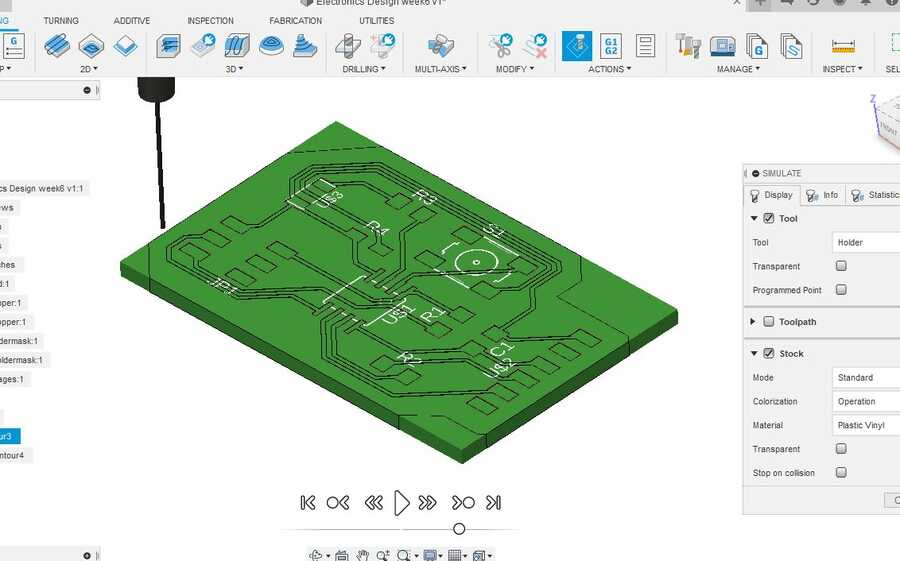
I have no issues with the milling path but I fail to find a way to “extend” the path and remove some more material to clear out some space between the traces…
In the preview of the milling job, I can see that first the trace will engrave but the traces look a little close to eachother, it will make the soldering more challenging. Iam also looking to explore more and find ways to add tabs for cutting when preparing the tool path. I would like to find out how to make my own 3d view of the components when designing a board so it can provide better visual information and also to build around it.
So to not lose more time, at this stage I find myself having to export the file as and stl import it in tinkercad and export it again as a .svg that I now can use in the same workflow as week4.
Preparing with Easel to create the g-code and candle to set up the job and run it.
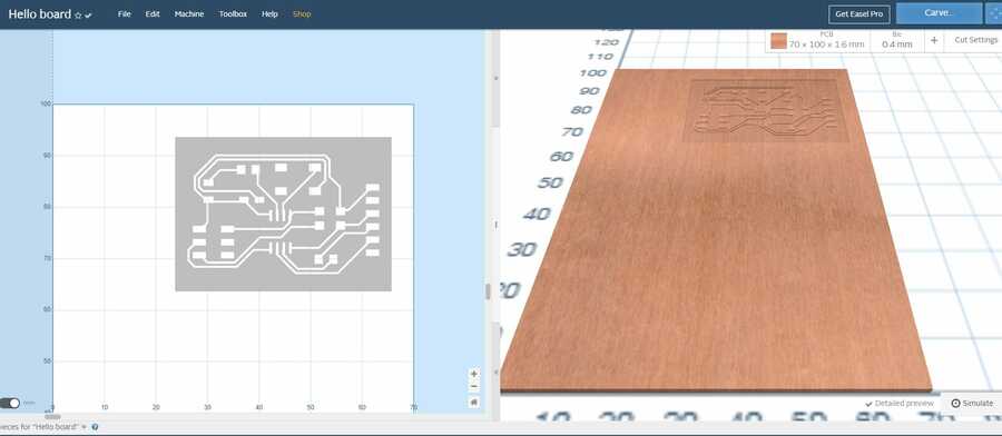
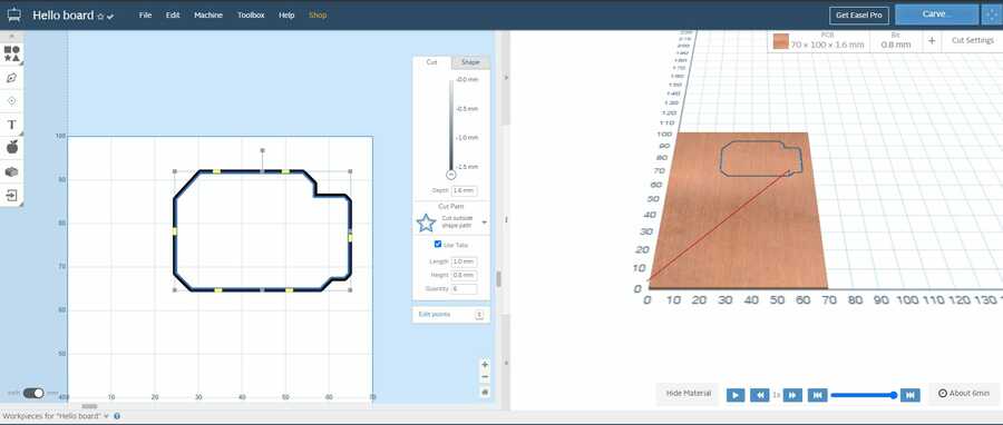
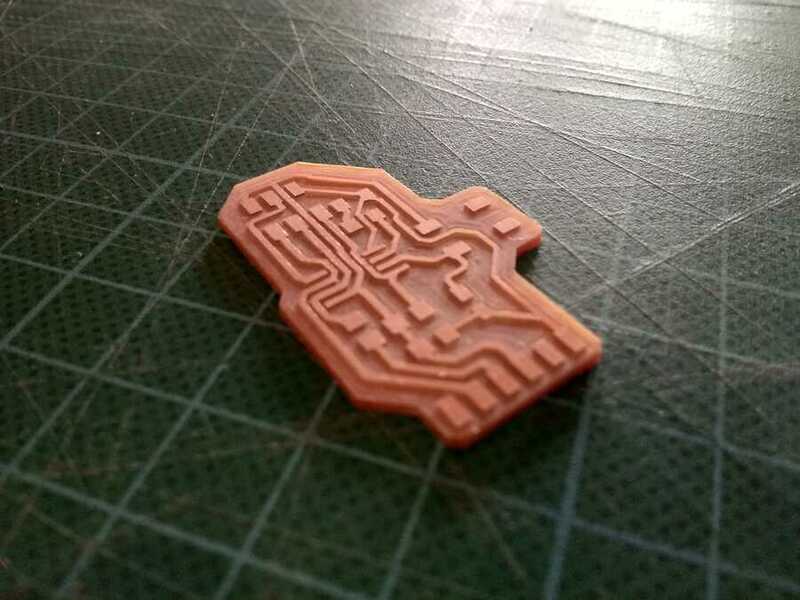
Here is the milling and result...
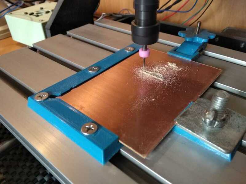
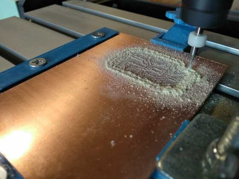
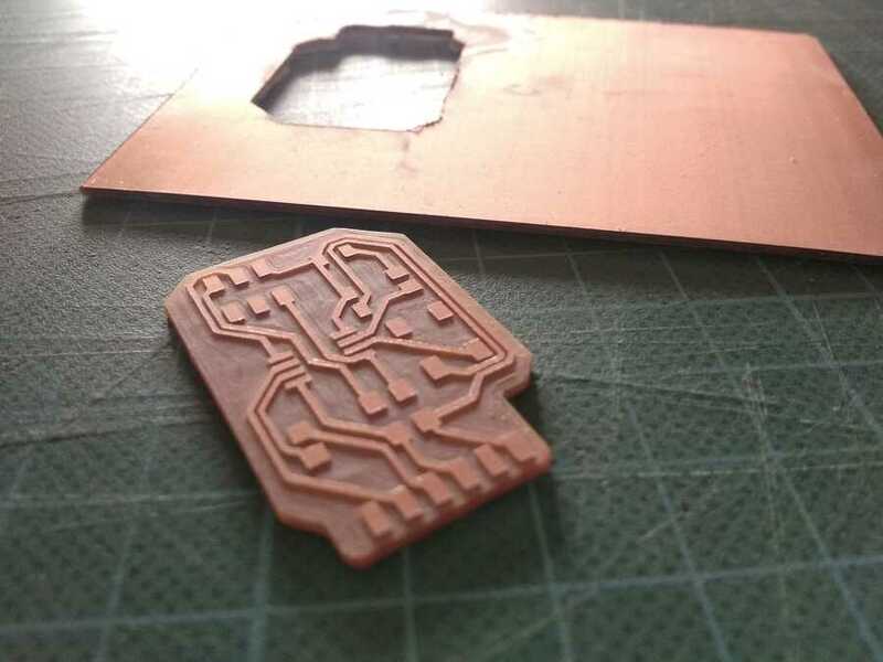
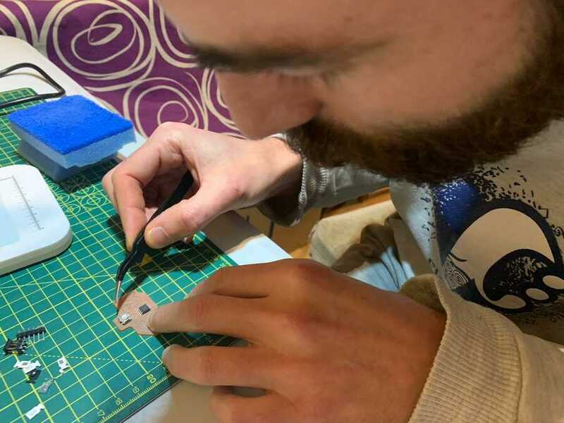
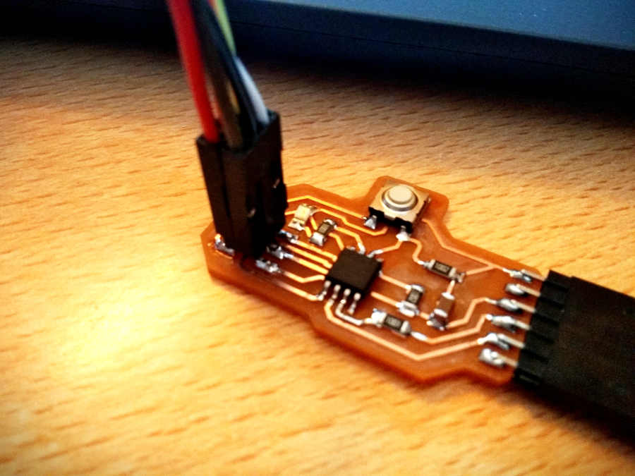
just after the cleaning I realised that I forgot to connect some of the pins and the voltage to the LED and the pulldown resistor….Back to fusion to fix all that and redo all the process to mill it again. This time I am using labels to connect the components
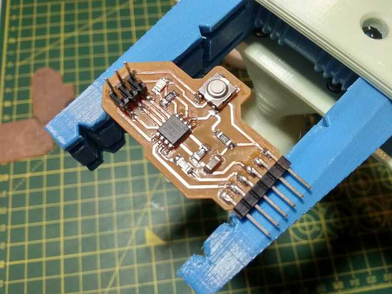
X2 boards after...Here is the third one, I think I can start soldering this one...(here are the .svg files traces and board)(Fusion files BRD and SCH
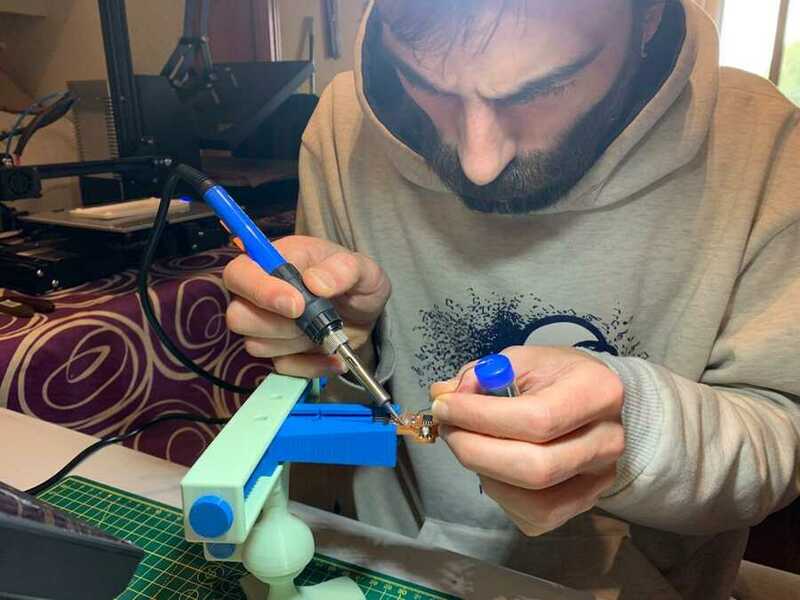
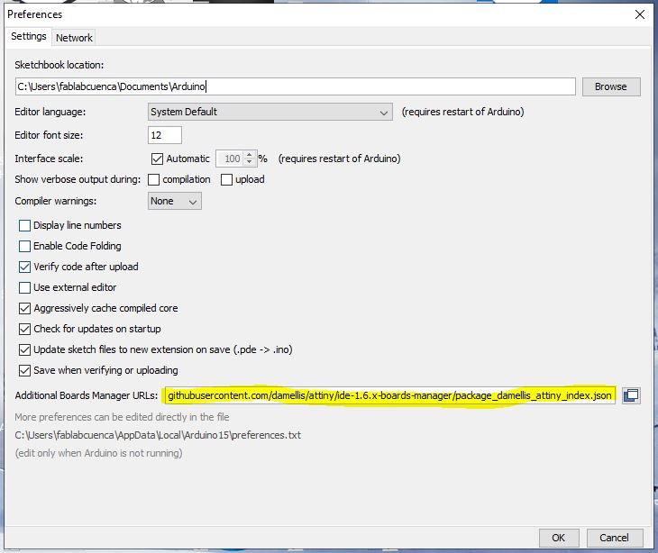
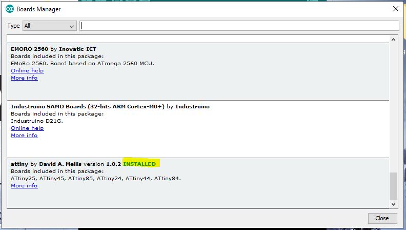
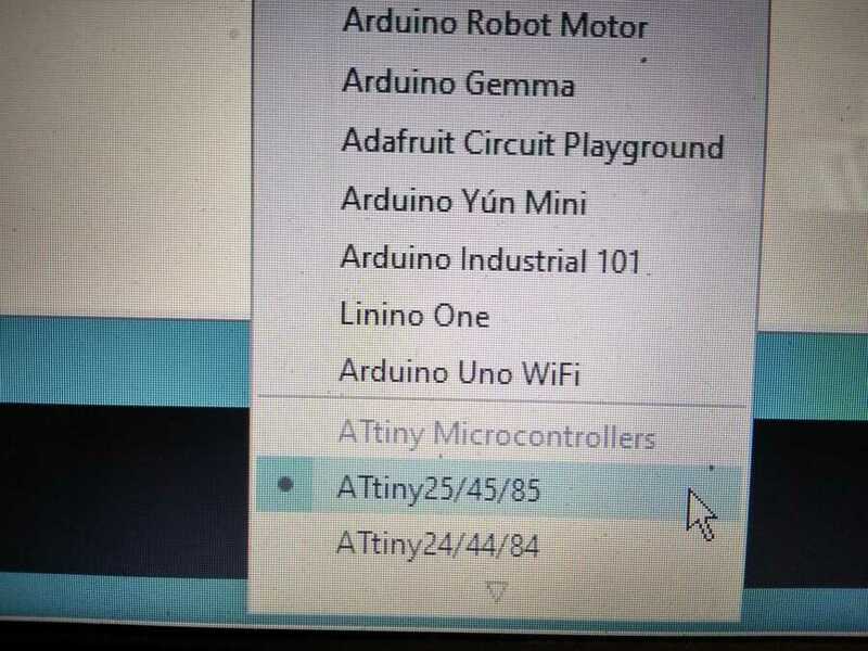
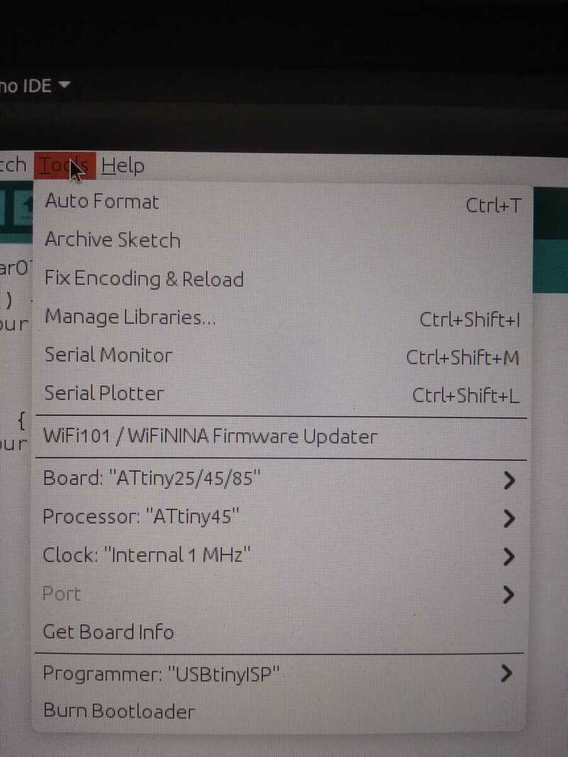
I am now trying to program it with the fabisp from 2weeks ago...To do that I needed to load the right library for the attiny in the arduino IDE, I followed this guide
I then conected the two borads with jumper cables and powered them separatly...
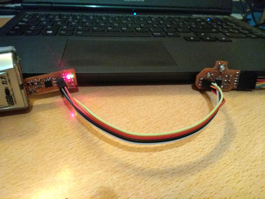
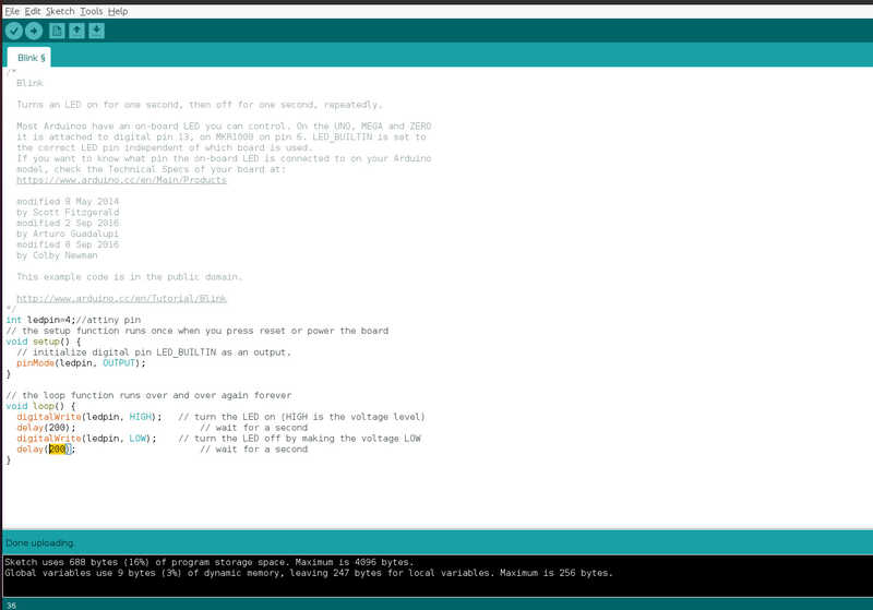
Loaded the "blink" sample test from the arduino IDE example. I set the LED pin by stating: "int ledpin=4;//attiny pin", changed the values of pinMode, digitalWrite and adjusted the delay time.
I am gathering info from this guy trying to understand a little more on how to write this type of code...
Here is the blink test
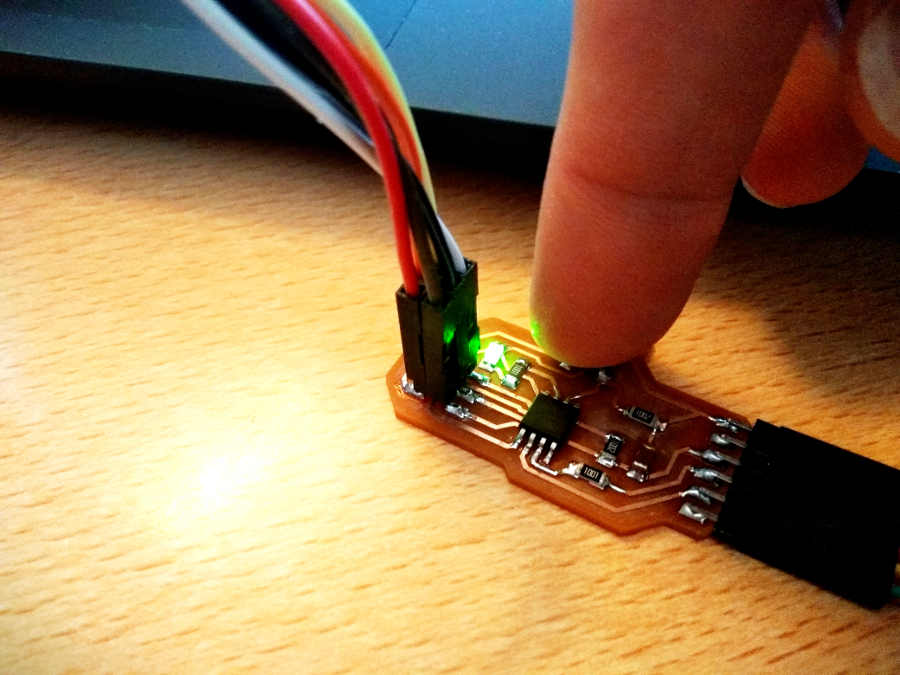
Here I am trying the button functionality again using one of the examples, I asigned the pins for the LED and button, in my case: button=3 and led=4.
Learning outcomes
Select and use software for circuit board designDemonstrate workflows used in circuit board design
Have you?
Linked to the group assignment pageDocumented what you have learned in electronics designExplained problems and how you fixed them, if you make a board and it doesn't work; fix the board (with jumper wires etc) until it does work.Included original design files (Eagle, KiCad, - whatever)Included a ‘hero shot’ of your boardLoaded a program and tested if your board works