The series of PCBs produced for this assignment consist of:
HelloD1614: Based on the ATtiny1614 and inspired by the Adrianino, the HelloD1614 is a simple board that can be used to test the features of the new ATtiny microcontrollers.
UPDI-3: This is a simple add-on board that allows programming of Microchip's new AVR microcontroller. The board functions as a bridge between the UPID target, and a serial communication.
FTDI-USB: The FTDI-USB is a board that implements functionality similar to that of an FTDI cable. Housing the FT230X, the board can basically convert from USB to serial and can be used for communication with your board, sensors, etc.
The designs come from the FabLab Kamp-Lintfort Wiki
Preparation
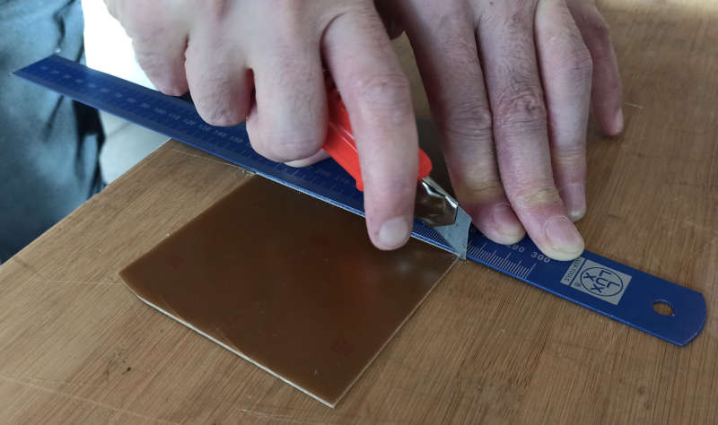
In this case I am using a FR1 plate, but because it does not fit well in the milling machine I decided to cut it in half, for that with a cutter and a ruler I pass the cutter several times (the goal is not to cut it completely with the cutter) to mark the break line.
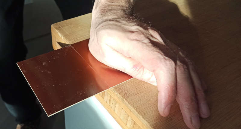
Supporting the break line on an edge, proceed to break the pcb with a movement that hits the part that is in the air.
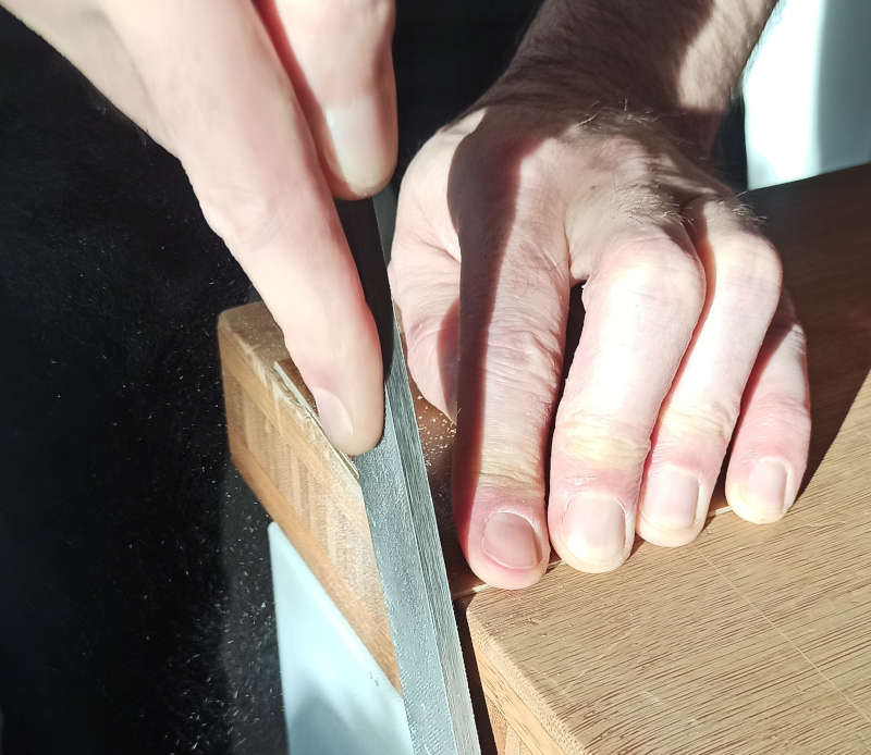
It is then necessary to file the imperfections in the break area to ensure that the plate will have a flat surface to rest on.
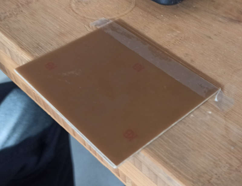
Double-sided tape is applied to the underside of the plate to ensure that the plate remains in place.
The plate is placed on the machining surface. In this part it is important to make sure that the plate is completely flat as this guarantees a correct milling, otherwise the mill may break or the plate will have areas that were not milled.
Milling
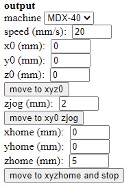
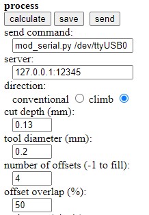
Before starting to machine it is necessary to prepare the file that is provided to the machine to perform the work, for that use http://fabmodules.org/ with the following parameters to make the traces.
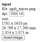
Input section
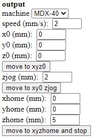
Output section
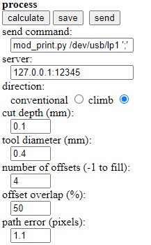
Process section
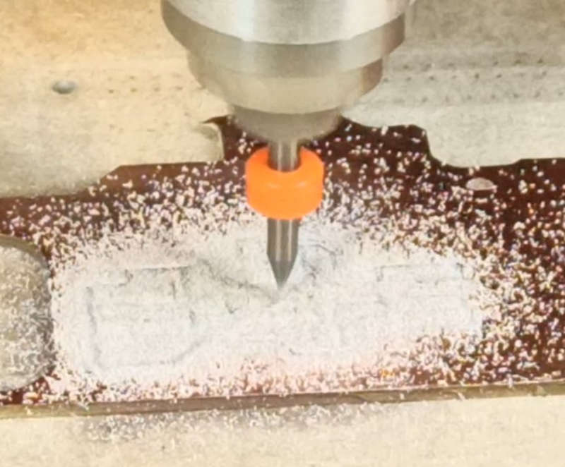
Milling was performed on a Roland MDX-40.
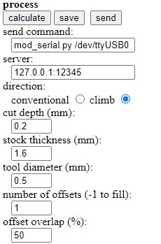
Use two tools to carry out the milling process, one to make the traces and the other to make the holes and cut the exterior.
Traces tool: 0.4 mm VHM
Holes and cutout tool: 0.8 mm VHM
With the milling file ready the next step is to adjust the height of the Z axis, this is one of the crucial parts that will determine if the pcb will come out well. There are many techniques that are used for this task, in this case the Z axis was approached to the surface of the plate while rotating the spindle (this must be done squarely so as not to damage the mill), once the Z axis is at the point on the machine interface the Z position is saved as the Z origin.
Once the machining process has started, you must be supervising that everything is going correctly and in case of a problem or emergency press the emergency button.
Post-processing
After the machining process it is necessary to remove the excess material produced by the machine.
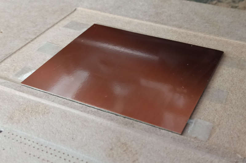
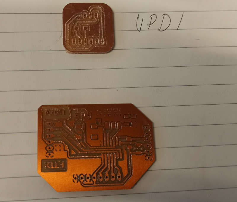
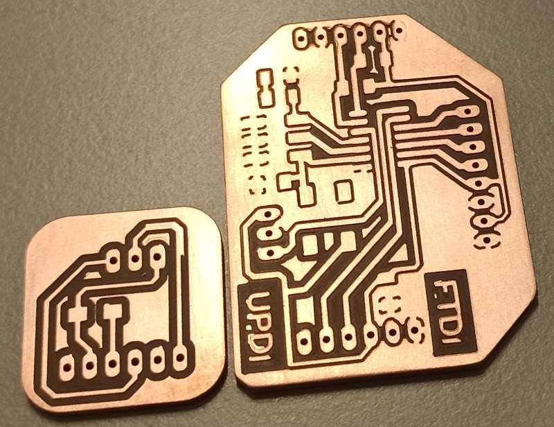
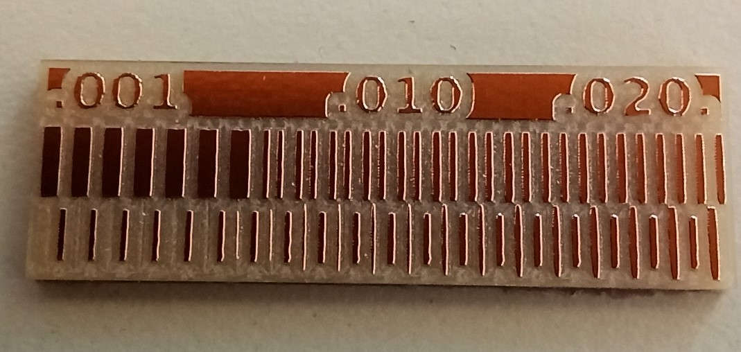
Using a fine wire sponge scrub the plate to remove the excess, then with a napkin wipe it with acetone, the result is the following image.
Soldering preparation
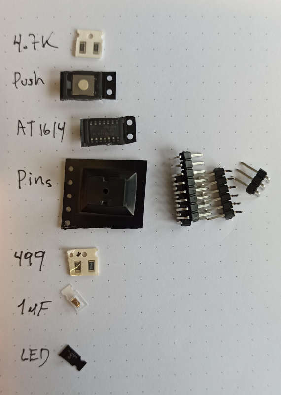
Before starting the soldering process is to select and organize the components because being so small it is quite easy to lose sight of them or confuse them with other components.
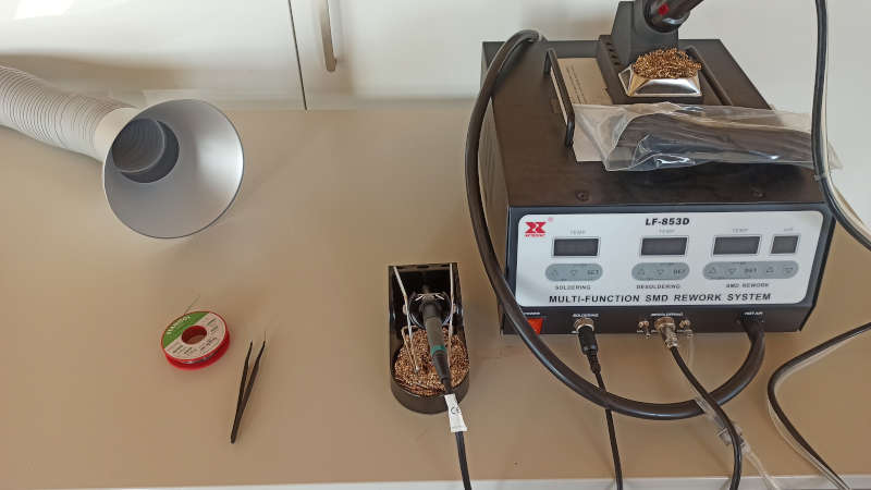
The soldering station must have an unrestricted free space and a smoke extractor.
Before I started soldering I decided to familiarize myself with the soldering station and soldering iron tip, and to find a temperature that I felt comfortable using and that would melt the solder properly.
Soldering
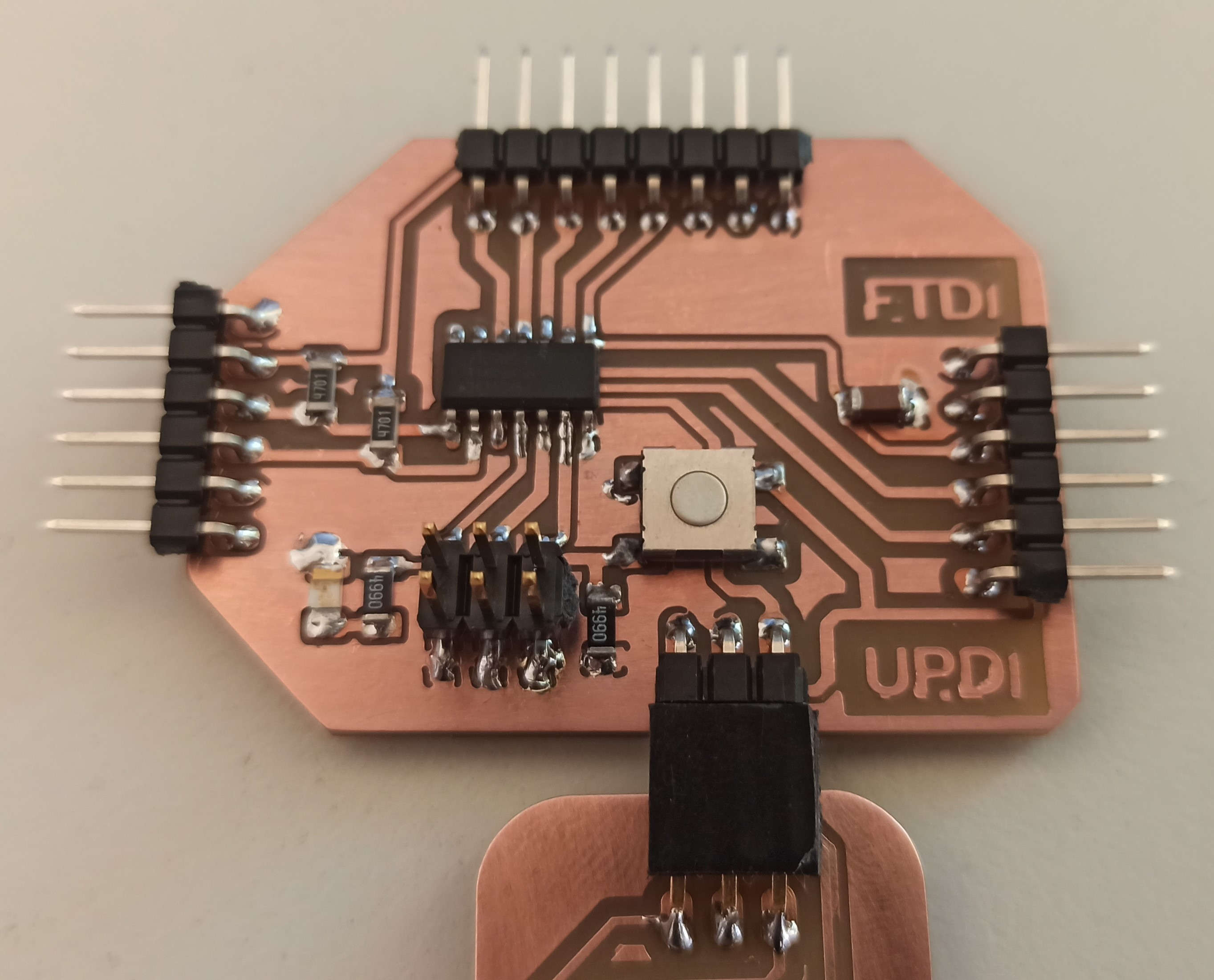
The soldering process was quite easy for me because I already have some experience with tin soldering but I had never soldered SMD components before, it was an interesting experience.
The technique I used to solder is the one that works best for me personally, which is to place a little tin in one of the places where the component is connected, then I take the component with the tweezers and position it near the place where it should be, while with one hand I hold the component with the tweezers with the other I heat the tin that I had previously deposited and when I see that the tin is melted I approach the component and I maintain it a few seconds until the tin hardens, in the other side of the component I heat the plate and the component and then I apply the right amount of tin and I remove the rubber.
The result is in the following image.
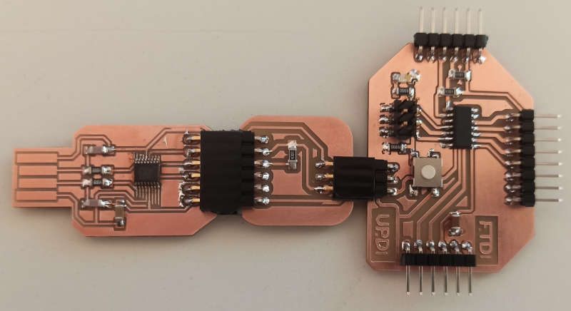
The process is basically the same for all the boards, so after repeating it 3 times I got the three pbc I needed.
Verification
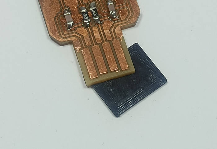
It is important to mention that for the FTDI-USB PCB it is necessary to remove the edges of the USB connection, this can be done from the milling process by increasing the number of passes, the problem with doing it that way is that it takes more milling time, so I decided to remove it myself with a Cutter Knife.
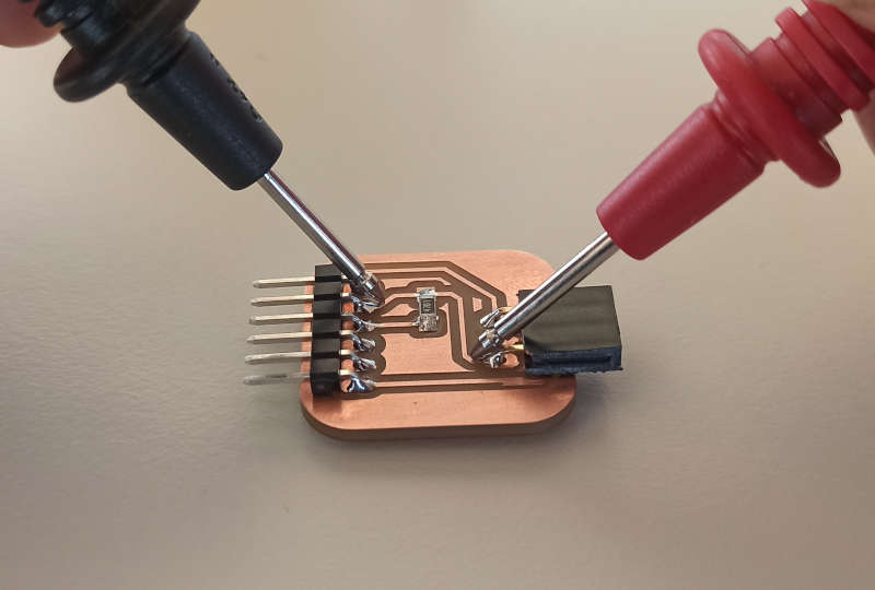
Without leaving the soldering station it is good practice to check the connection of the components using a multimeter, in case of a problem it is necessary to correct it.
Test
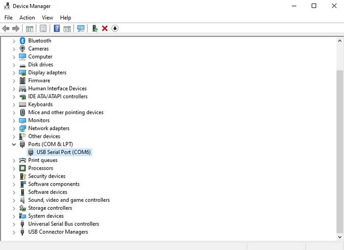
To test that everything is working properly I connected the PCBs to my computer to see if it recognized them.
The test connection is (Computer)<->(FTDI)<->(UPDI)<->(HelloD1614)
It does in fact detect the PCB on the COM6 port.
Group Assignment
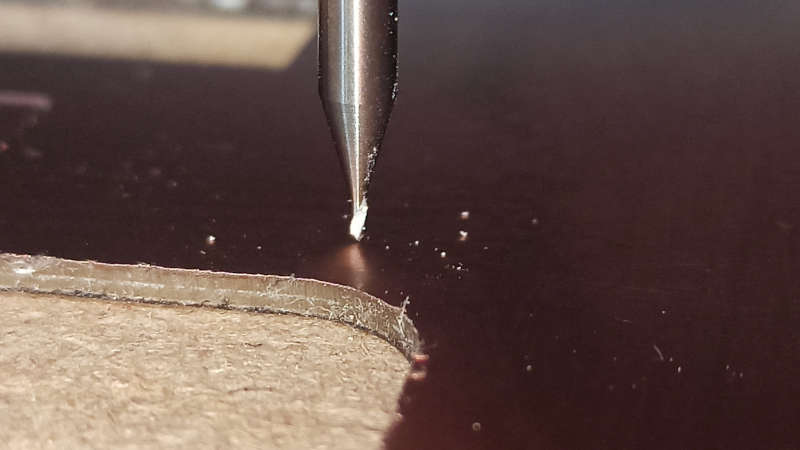
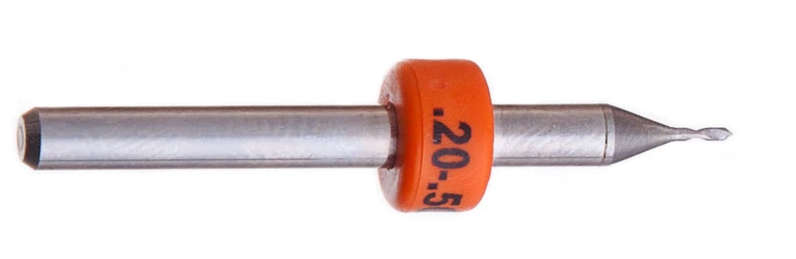
Inspired by the idea of one of my instructors (Ferdi) to produce high speed pcb's without tool changes I decided to experiment a bit with a 0.2-0.5 mm V-point tool.
The test parameters are as follows.
To make the traces: Output section
To make the traces: Process section
To make the outer cut I used the same parameters in the output section and only changed those in the process section.
Here is a video of the milling process and the result.
The result is very promising but there is still room for improvement, more experiments will be done soon to better adjust the parameters.