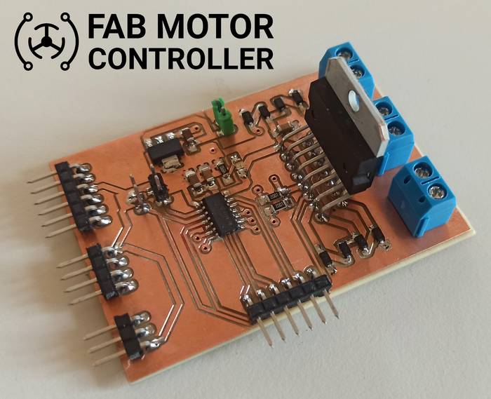
Fab Motor Controller
This tutorial arises thanks to the assignment of week 12 (Output devices) of the Fab Academy, assignment in which after having made a motor controller that did not work (and did not know why) I decided to make one completely from scratch, with some improvements over the previous version.
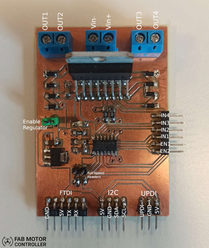
The idea of this tutorial is to describe in more detail the whole process to replicate the controller which I call FAB MOTOR CONTROLLER, it is a controller based on the L298N driver with an integrated ATtiny1614 which is responsible for interacting with the driver.
After the failure with the previous controller that did not work I had very clear some features that I would like to implement in the Fab Motor Controller, such as adding a 5v voltage regulator that could be enabled / disabled to use the voltage of the power supply from the motors, and expose the control pins of the driver to use an external controller instead of the integrated on the board (this because in the previous one the integrated ATtiny1614 died). I also wanted to improve the pcb layout and distribute the components in a better way.
- ATtiny1614 microcontroller onboard
- Voltage regulator NCP1117 maximum input 20V, fixed output 5V
- L298N driver to connect two motor outputs up to 2A per channel
- Header to enable/disable the voltage regulator
- Connection pins for using an external controller
- FTDI, I2C and UPDI communication pins
| Device |
Manufacturer part number |
Quantity |
| ATtiny1614 |
ATTINY1614-SSFR |
1 |
| L298N |
L298N |
1 |
| 10uF Capacitor ceramico 35V |
587-3007-1-ND |
2 |
| 100nF Capacitor ceramico 35V |
CL05C101JB5NNNC |
2 |
| LED |
160-1169-1-ND |
1 |
| Schottky Diode |
MBRS140T3G |
8 |
| Male through-hole header |
S1011EC-40-ND |
19 POS |
| Screw terminal 2 Positions |
1760510000 |
3 |
| 10k resistor |
RC1206FR-0710KL |
2 |
| 1k resistor |
RC1206FR-071KL |
1 |
| NCP1117 Linear regulator 5V |
NCP1117ST50T3G |
1 |
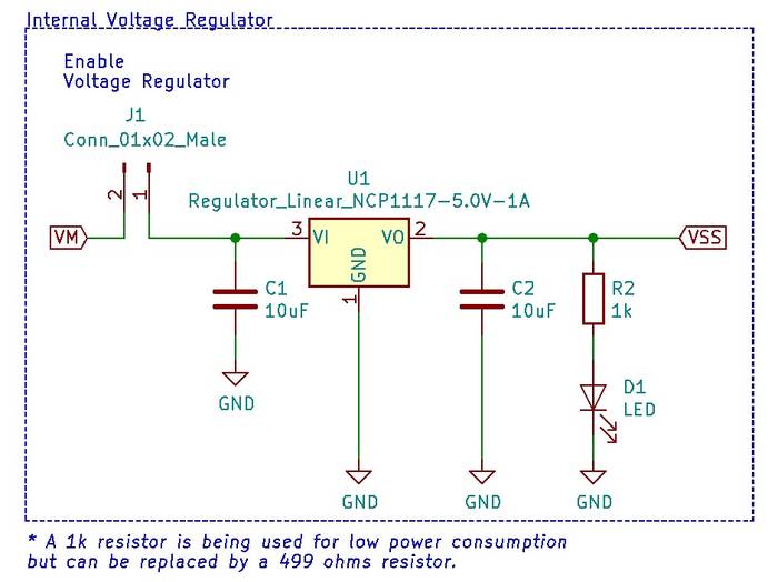
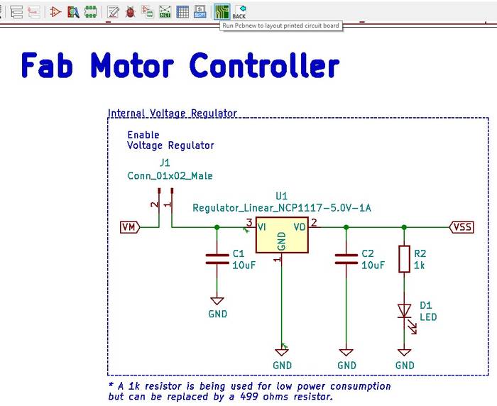
The voltage regulator on the board is the NCP1117 which has a maximum input voltage of 20V and a fixed output voltage of 5V, to have the ability to enable/disable a Male Pin Hader was added on the input side, in addition to the filter capacitors, a resistor and an LED indicating that there is 5V in the circuit.
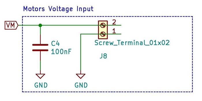
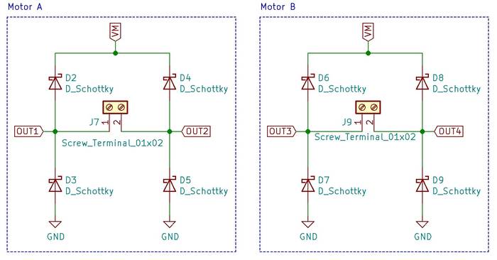
Then we designed the input voltage part for the motors which is quite simple and contains only a capacitor and a 2 position Screw Terminal.
The connection part of the motors contains a diode bridge that at first glance seems to be in the wrong position but in reality they are fine as they function as protection diodes and not control diodes, so the position may seem a little strange.
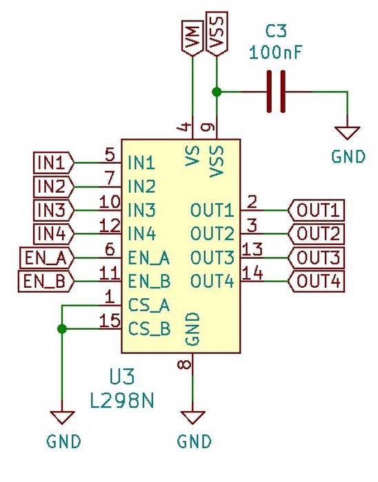
The L298N driver has two pins per channel to control the direction of rotation of the motors, so IN1 and IN2 control output OUT1 and OUT2, just as IN3 and IN4 control OUT3 OUT4. Also the driver has the possibility to measure the current between the outputs but this time I decided not to use them so they are only connected to GND.
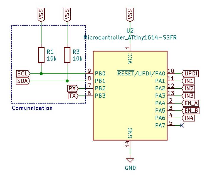
The ATtiny microcontroller has the right amount of pins to use UPDI, FTDI and I2C and all the necessary control signals for the driver so it fits perfectly as a controller, the connection looks like this.
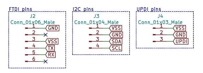
And the communication pins are distributed like this.
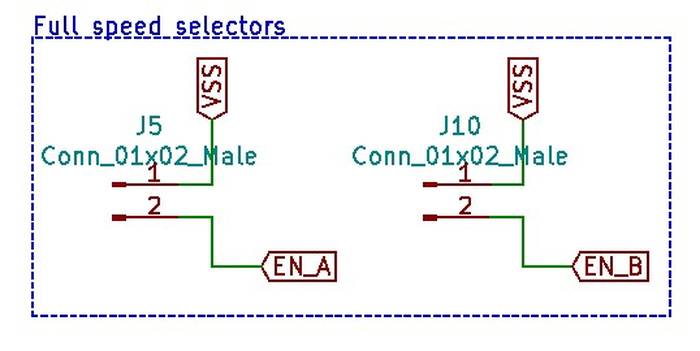
I added a header that allow to activate 5V on the inputs EN_A and EN_B that control the speed of the outputs, connecting those inputs to 5V the driver interprets them as full speed.
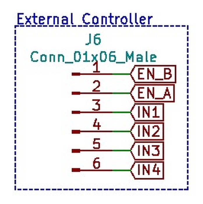
And finally the connectors to be able to use an external controller, in case something happens to the ATtiny1614 or if you just want to use another board to control the driver.
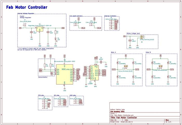
The schematic overview is as follows.
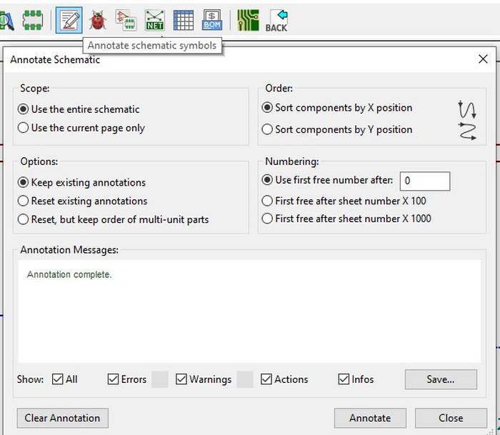
With the schematic finished in KiCad it is necessary to create the annotations of the components you can do it manually if you like but there is a functionality that does it for you, at the top in Eeschema there is an option called Annotate Schematic, it will open a box and just press Annotate.
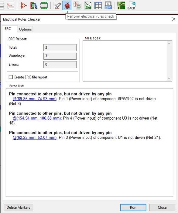
In KiCad it is also possible to check that all electrical connections are OK using the "Electrical Rules Checker" tool which is located at the top, it will open a box where you press Run and it will tell you where there are connection problems. In my case it tells me that there are 3 pins that are connected but it is not being driven by any pin, this is because it interprets the labels as SOURCE or GND, that is why there are three errors that correspond to VM (Voltage input for the motors), VSS (5 Volts) and GND, this is not really a problem but if we do not want that error to happen we must add PWR_FLAG for each SOURCE and GND, but not doing it does not affect the real connection of the circuit.
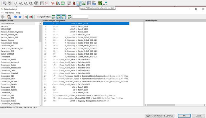
Now we have the components written down and verified the connections, now it is time to associate them with a footprint which is the way the components look physically, the footprints depend on the physical components you have available and their dimensions. To assign the footprint in the upper part you find a button called "Assign PCB footprints to schematic symbols", in this project the assignments look like this.
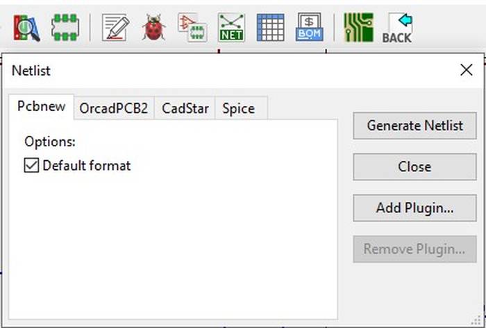
Before starting to work on the pcb routing we must associate the schematic components with the pcb components, this is done by generating a Netlist, at the top there is an icon that says NET when we click on it a box appears in which we select the Pcbnew tab (the PCB design tool integrated in KiCad), click on Generate Netlist, select a location to save the netlist file (usually in the same address of the project), click on Ok and ready, Pcbnew will use that file to associate the components and keep updated the pcb based on the changes made in the schematic.
At this point everything is ready to start doing the layout and routing of the pcb, for that press the button at the top called "Run Pcbnew ...".
You will find a black canvas but don't worry it is only a matter of loading the Netlist that was generated before and all the components with their respective footprint will appear. At the top of Pcbnew is the icon that says NET when you click on it a box will appear in which you will look for the file that you generated before and finally press the button Update PCB.
This action will load all the footprints, before starting to adjust the position and distribution of the components it is important to adjust the size of the tracks in the circuit, this because there are sections of the circuit where the track must conduct more current.
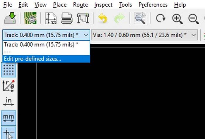
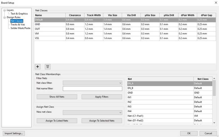
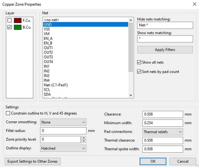
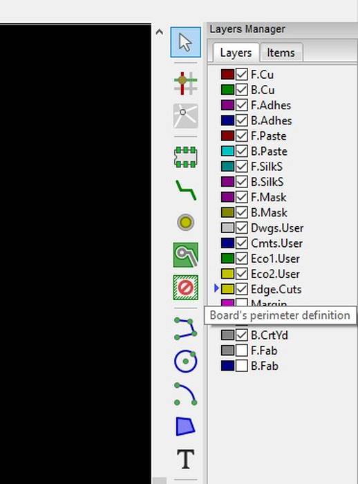
To adjust the sizes of the tracks based on the type of signal to which they correspond it is necessary to associate the properties of the track with a type of signal, this can be done thanks to the net-classes, this option can be found in the place shown in the following image.
A window appears that by default opens the "Track and Vias" section, we simply go to Net Classes, in this section we can create several Net-classes with different characteristics, pressing the plus symbol we can add all the necessary ones, in this case I decided to create 4 net-classes in addition to the default one which is modified. Because the available vias in the Lab of 0.6mm the option Via Drill corresponds to 0.6mm, Via Size is the upper part of which the Via that we place will make contact, I decided to place a value a little more than double the Via Drill Size since pressing it expands a little, this way I make sure that it has contact with the track and that it will not make contact with another track to which it does not correspond.
In the lower right part we can associate our net classes with a Net, so GND is associated with GND, VM is associated with VM, etc, so when a connection is made in that net it automatically takes the properties of the Net class that we associate.
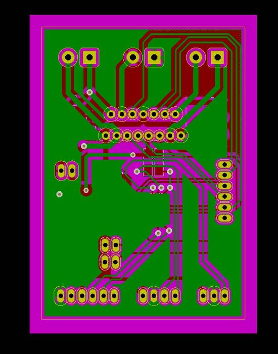
With the experience of the previous controller that did not go so well I already knew that this pcb should be two-sided, a mistake I made in the previous design was to make connections at the top and bottom of the Screw Terminals which made it impossible to solder it on the top because the terminal covered it, so I started from that part and keep those connections at the bottom.
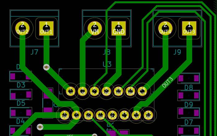
For the routing at the bottom and to minimize the number of vias I decided to take advantage of the through-hole components to make the through-hole
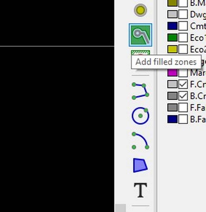
Because the driver can conduct up to 4 amps of current the GND must have enough space to dicipar heat, KiCad allows us to create filled with a Net that we select, that function is found in the right side panel as "Add filled zones".
Now we can draw figures like a square and associate it to a Net in this case GND.
After drawing the area we want to fill the result is as follows.
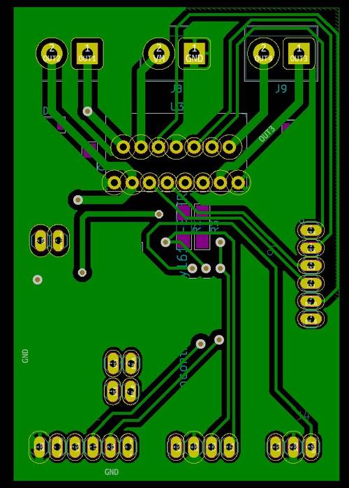
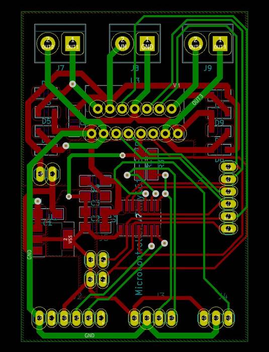
The routing at the top looks like this.
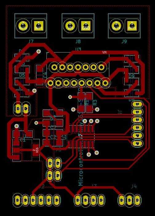
We repeat the process of creating filled areas associated to a Net, we are not limited to a single area, we can create several associated to different Nets, at the top I decided to create two areas one for VM (The input voltage for the motors), a smaller one for the 5V output of the regulator.
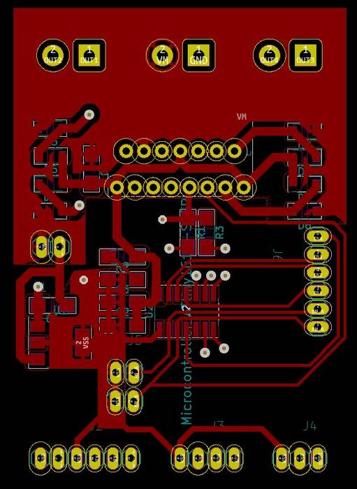
With both sides of the pcb ready the result is as follows.
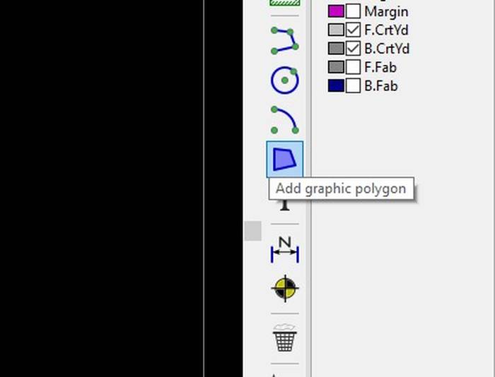
The next step is to add the edge where the pcb ends, in KiCad it is known as "Edge Cut", to use it you need to switch to that layer in the right side panel.
And with the "Add graphic polygon" tool we delimit the edges of the pcb.
Finally, I personally like to add a margin for the pcb images to have a margin for machining when exporting them.
This can be achieved by changing to the "Margin" layer
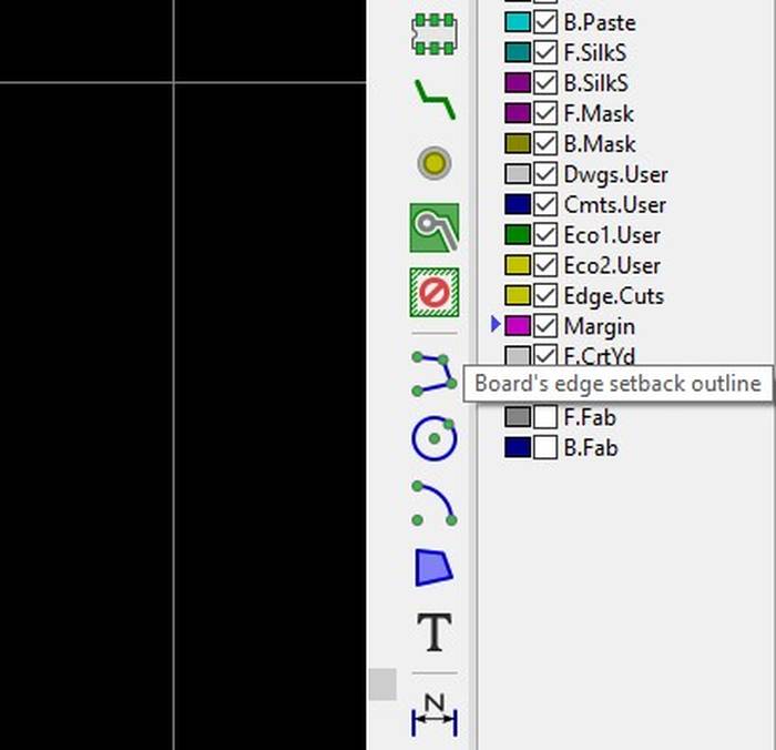
Drawing a polygon that delimits the margin.
The result will look something similar to this.
The next thing will be to inspect a little how the pcb looks in 3D, this can be achieved in the top menu View->3D Viewer or by pressing "Alt+3".
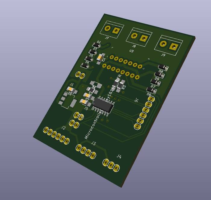
Everything looks fine in the 3D view.
Exporting images for milling
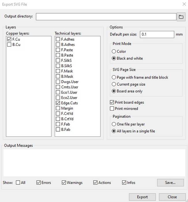
In the menu File->Export->SVG we can export the pcb as SVG but remember that it is a TWO SIDED PCB so it is necessary to export one image for the top side and another one for the bottom side.
To export the top side of the PCB we check the Copper Layer "F.Cu" which represents the front side, in the "Technical layers" panel we deactivate everything except "Edge.Cuts", in Print Mode we check "Black and white", in "SVG Page Size" we select "Board area only", we also check the option "Print board edges", the configuration to export the top side looks like this.
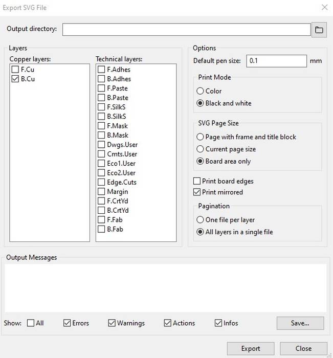
For the bottom side of the pcb we select the "Copper Layer" with the name "B.Cu", we uncheck the "Edge.Cuts" checkbox and change to "Print mirrored" option, the configuration to export the bottom side looks like this.
Now we have two files in SVG format, both contain information of the traces, holes, and the top one contains the border, those files need to be processed to separate the traces, holes and the border, there are many ways to do it.
Preparing images for Gcode generation
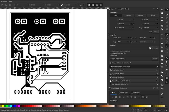
The images that we export can be processed as vectors or they can be converted to PNG and worked as bitmaps. This time I am going to prepare them as PNG.
To do this we start by opening the SVG file at the top with any vector program, in this case I am using Inkscape but it can be any other, we will simply use the software to export the PNG version at a value of 1500 dpi.
In Inkscape in the "Export area" section we select "Page", we can change the units to millimeters "mm" to know the size that will have the pcb, in the "Image size" section we put "1500 dpi", we select the location where we want to save the image and with what name, and finally we press "Export".
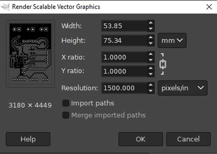
Another way to do this is by opening the SVG image with GIMP, when we do this we get a box to render the SVG, here we can also change the unit to millimeters and in "Resolution" we set "1500 pixels/in" which is exactly the same as "1500 dpi" (Pixels per inch).
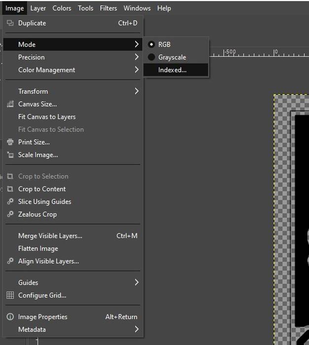
With the image in PNG format in GIMP, it is necessary to change the mode to Indexed to have only two colors in the image, in this case black and white.
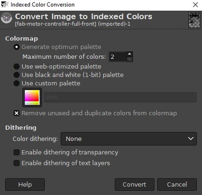
We configure the Indexed Color Conversion window as follows.
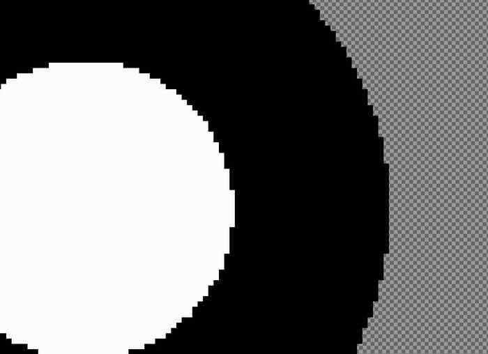
If we zoom in on any part of the image before applying indexed we will see that there are gray tones in the areas that go from white to black.

After applying indexed we will have only black and white.
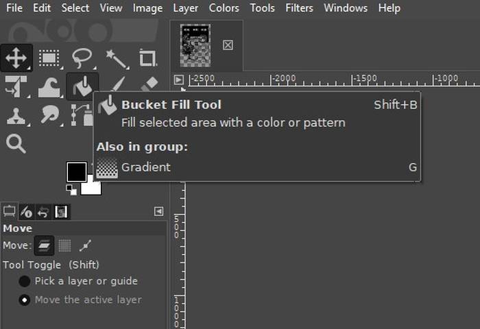
With the Bucket Fill tool we can fill with white color the missing zones.
The result is as follows.
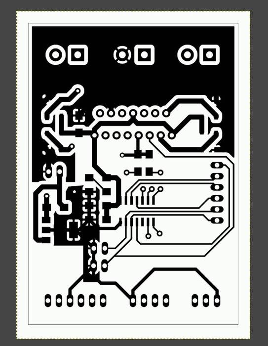
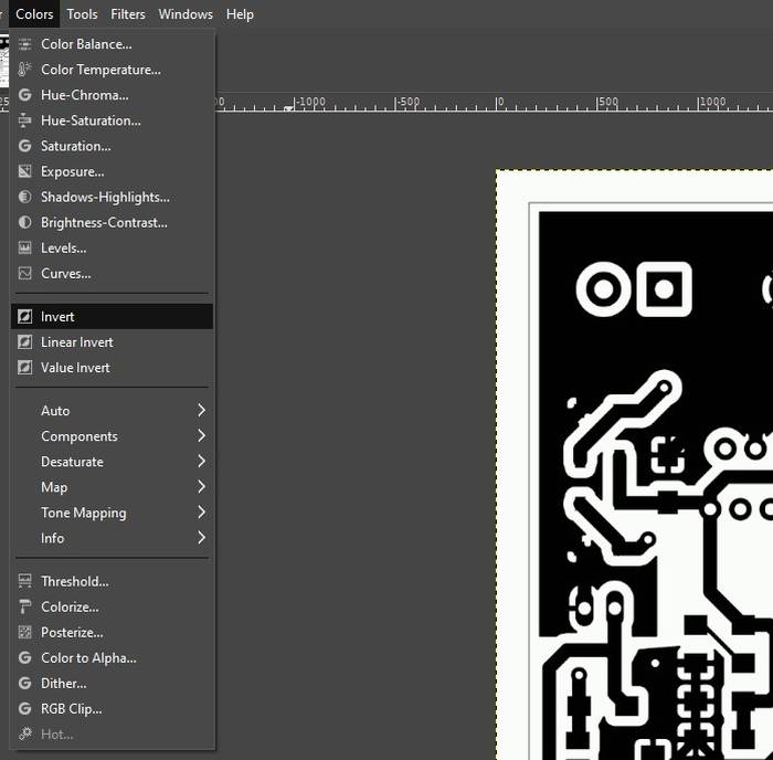
The image processor that will generate the machine code for the milling interprets the black as the areas to remove and the white as the areas to keep, in this case we want to keep the traces and remove the holes and the border, and if we notice well our image is the opposite, but this is easily corrected, in the "Colors" menu in the top menu we find the function "Invert" that inverts the image, just what we need.
After applying the color inversion the pcb looks like this.
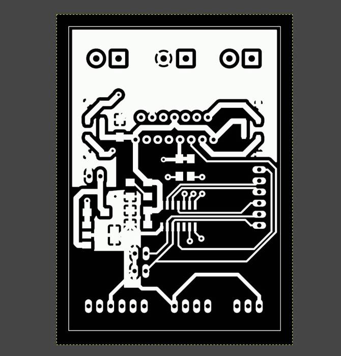
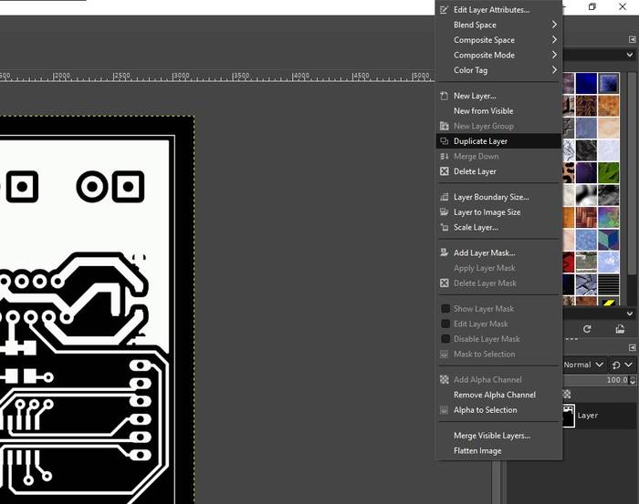
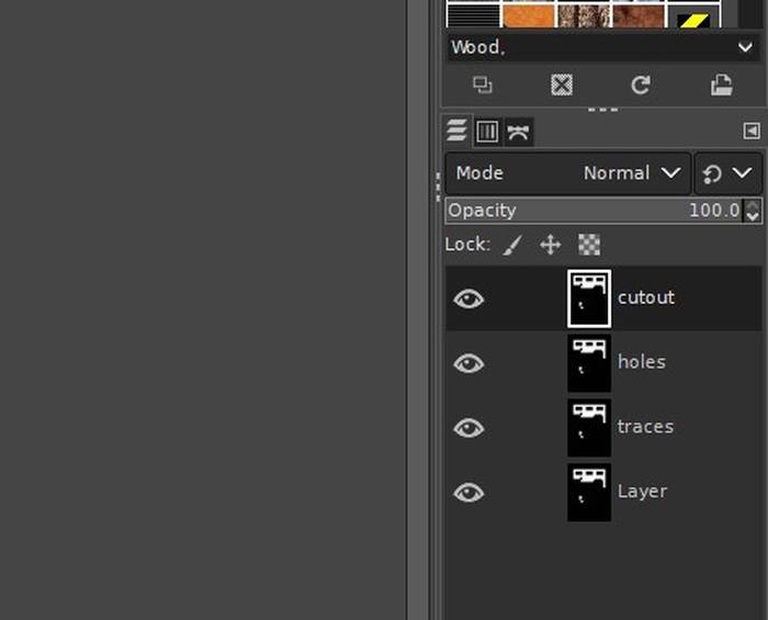
Now we need to separate the traces, holes and the border, the way I do it is that I duplicate the layer until I have equal layers that corresponds to the original layers, the traces layer, holes layer and the border layer.
which results in this form.
In the "traces" layer using the Bucket Fill tool we fill the border with black and we are left only with the traces, although you can leave the border it will not affect anything but if you remove it you can save a little time.
If you don't see any changes leave visible only the layer you are working on.
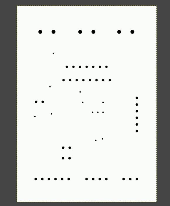
In the holes layer we should fill everything and keep only the holes in black, remember that what is in black is what is going to be removed and we just want to remove the material to create the hole, the result should look like this.
We only need the "cutout" layer in which we must fill in white up to the edges of the pcb area.

With all the layers ready it is a matter of exporting them individually, that means that we have to have visible only the layer that we are going to export.
We must export them in PNG, with the following configuration.
For the lower part the process of preparing the image is exactly the same with the only difference is that only the traces are needed, because the holes and the cut will already be done.
Generating the Gcode for milling
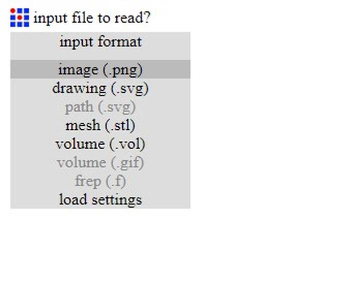
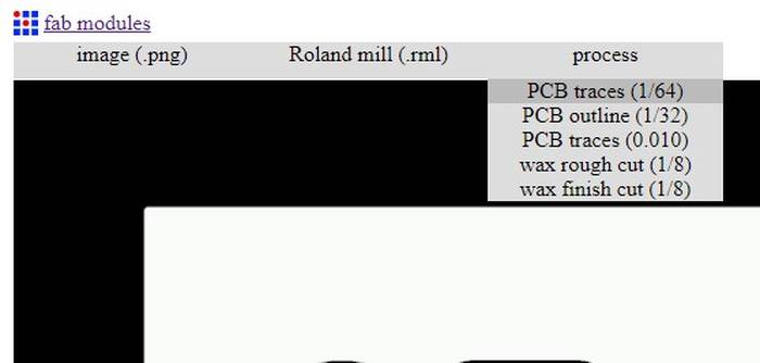
This can be done in many ways using one of the many tools available, in this case I will use FabModules.
We start by loading the traces image.
In the "ouput format" option we select "Roland mill", this is because the milling process will be done on a specific Roland machine, the SRM-20, but if it is any other type of machine, Gcode can be generated.
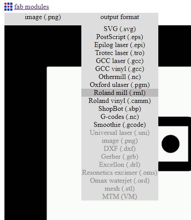
In the next option "process" we select "PCB traces (1/64)".
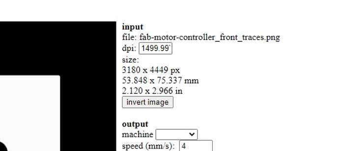
In the right panel we can see the measurements of the area to be machined.
I want to warn you that the following configurations depend a LOT on the machine and the End Mill you have, so you must be careful in the values you use. In my case the End Mill I am going to use is this which is a V-shpe type from 0.2 to 0.5 mm, it is a tool that I have done many tests with and I am completely sure that it works perfectly at high travel speeds, I even did a test on a Roland MDX-40 at 20mm/s with this tool, you can see a video of that test here. Although the tool can go very fast the Roland SRM-20 can only spin the Spindle up to 8000 RPM so I use very conservative values, plus it gets a very good finish in less time as this process is usually done at 1mm/s or 2mm/s depending on the machine and the quality of the End Mill.
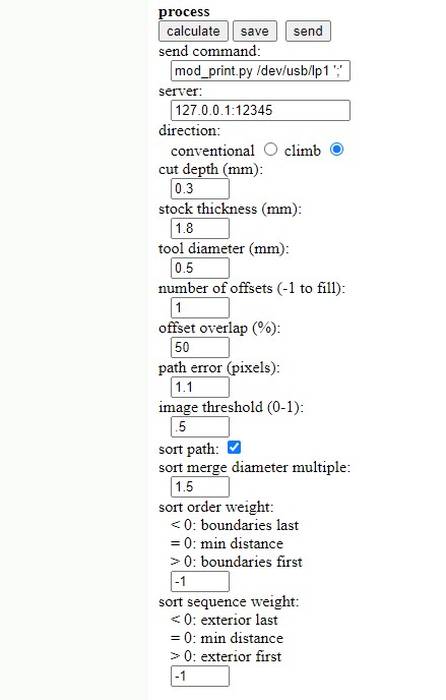
Press "calculate" and if all the paths seem to be ok press "save".
At this point we should have four files, one with the top side traces, one with the holes from the top, one that corresponds to the edge and one for the traces from the bottom side of the pcb.
As I mentioned before the machine I am going to use is a Roland SRM-20 so the software to control and send the files is VPanel.
Before we start machining we place double sided tape on the bottom of our board, this is so that it will hold well to the surface of the machine and will not move during the machining process.
Because of the type of tool I am using I don't need to change it during the process of traces, holes or cutting, so I load the three files at the same time, but it is important to place them in order, first the machine must do the traces, then the holes and finally the cutting, this is because if it does the cutting first the pcb will be prone to move during the work of traces or holes.
The result of the first side looks like this.
After that we carefully remove our pcb, we remove the remains of pcb from the bottom side and we put double sided tape on the top side because now we are going to machine the bottom side.
The next step is very important, because the pcb must be aligned to the previous position, there are many ways to do it, some people use reference pins but in my case I don't have those, so I will do it aligning it with the view, using as reference the edge of the PCB, I must make sure that it is at the same distance in all the margins. It is also important before placing the pcb on the other side to remove all the tape remains to make sure that when we place it on a flat surface.
Before launching the traces file on the lower part, you have to adjust the Z again, but ONLY THE Z. The result is as follows.
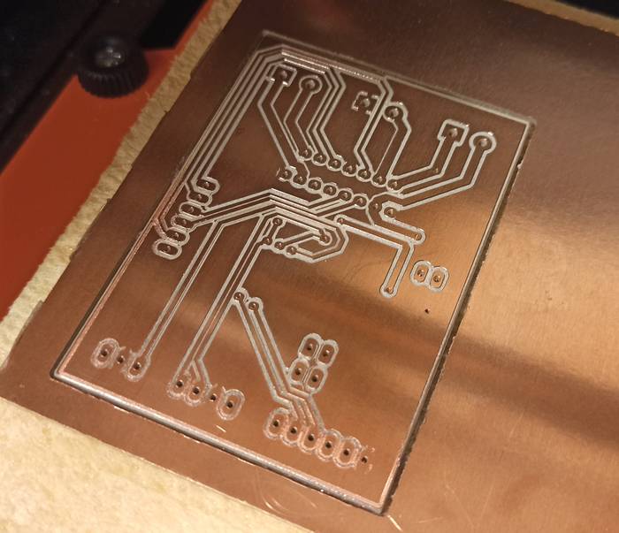
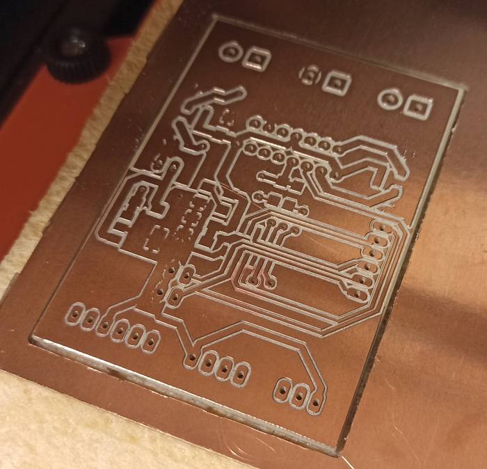
The PCB looks very good, the bottom traces seem to be very well aligned with the top traces.
Now check with your eyes that all the traces are OK and that there is nothing like a broken trace, or a trace that is making contact with a trace that should not be.
Component soldering process
Personally I like to start soldering the SMD components from the center of the pcb to the ends, I feel it gives me more working space as some components are taller than others and sometimes it is difficult to solder because they cover part of the space needed by the Solder Tip.
The solder used for soldering was a 0.5 mm diameter STANNOL and a solder iron type B, there is nothing special about the choice of solder or iron tip.
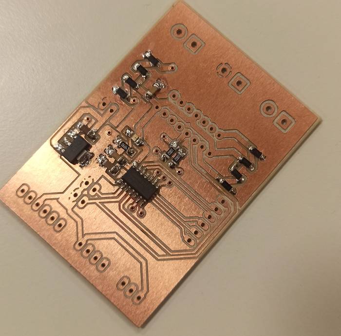
The result after soldering all the components is as follows.
- KiCad
- Inkscape
- GIMP
- FabModules
- VPanel