Electronics Design
Assignment Requirements:
- Use the test equipment in your lab to observe the operation of a microcontroller circuit board (in minimum, check operating voltage on the board with multimeter or voltmeter and use oscilloscope to check noise of operating voltage and interpret a data signal)
- Document your work (in a group or individually)
- Redraw one of the echo hello-world boards or something equivalent, add (at least) a button and LED (with current-limiting resistor) or equivalent input and output, check the design rules, make it, test it.
Learning Outcomes:
Steps in General:
- Step(1): Using Test Equipment
- Step(2): Designing the echo hello-world board on KiCAD
- Step(3): Extracting the CAM Files
- Step(4): Fabricating the Board
- Step(5): Stuffing and Soldering the Board
- Step(6): Programming & Testing
Steps in Details:
Step(1): Using Test Equipment
We have used the Oscilloscope, Function Generator and digital multimeters and learned how to operate each equipment and its functions and applications. Press here for the group documentationStep(2): Designing the echo hello-world board on KiCAD
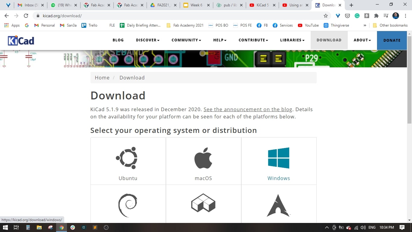
- First, I have downloaded and installed KiCAD for Windows
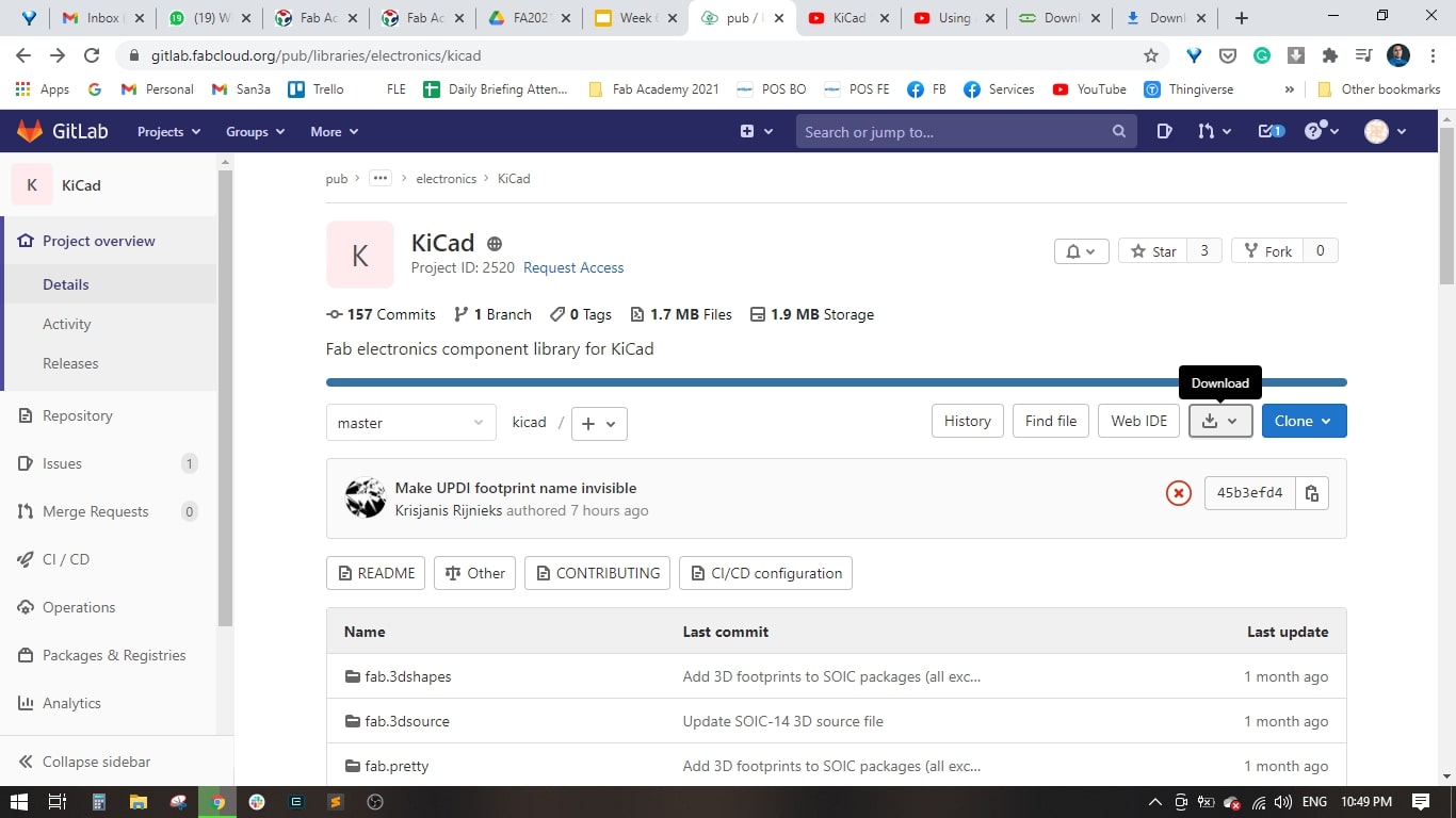
- I dowloaded KiCAD's Fab Library from the FabCloud, Kris did a great job in making a fab library for both Eagle and KiCAD, it has most of the fab academy inventory.
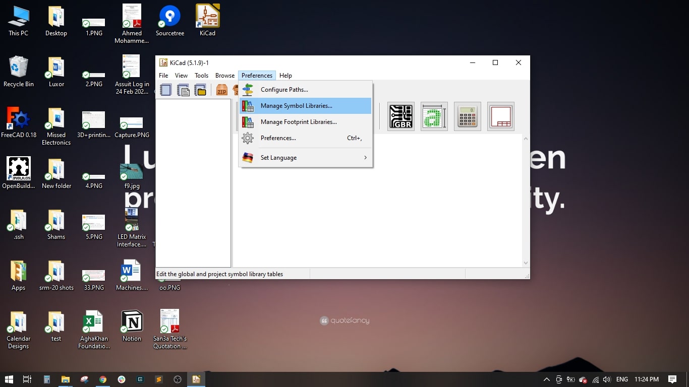
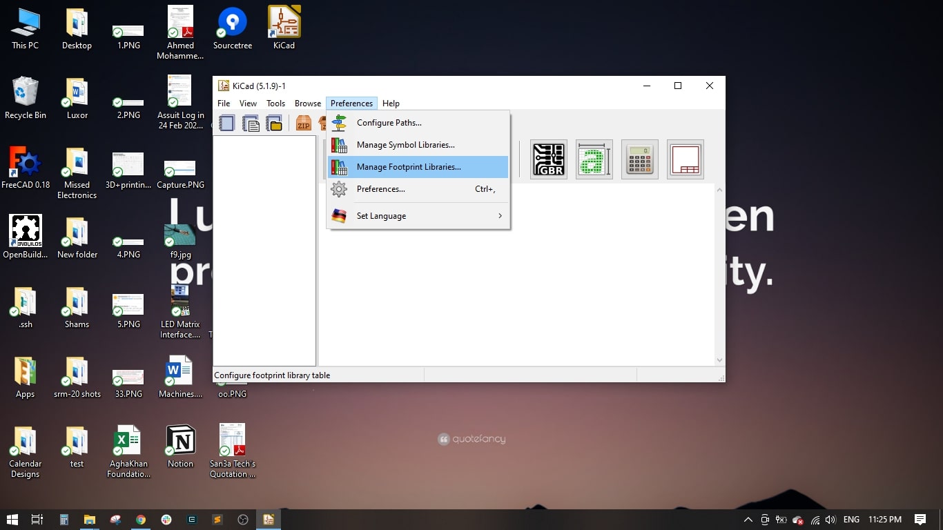
- In KiCAD, I selected Manage Symbol Libraries from the Preferances menu.
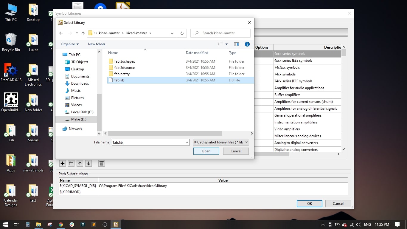
- I added the fab.lib to include all the symbols into KiCAD Schematics.
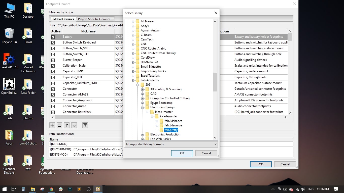
- Also I have selected Manage Footprint Libraries from the Preferances menu.
- I added fab.pretty to include all the footprints to the KiCAD routing environment.
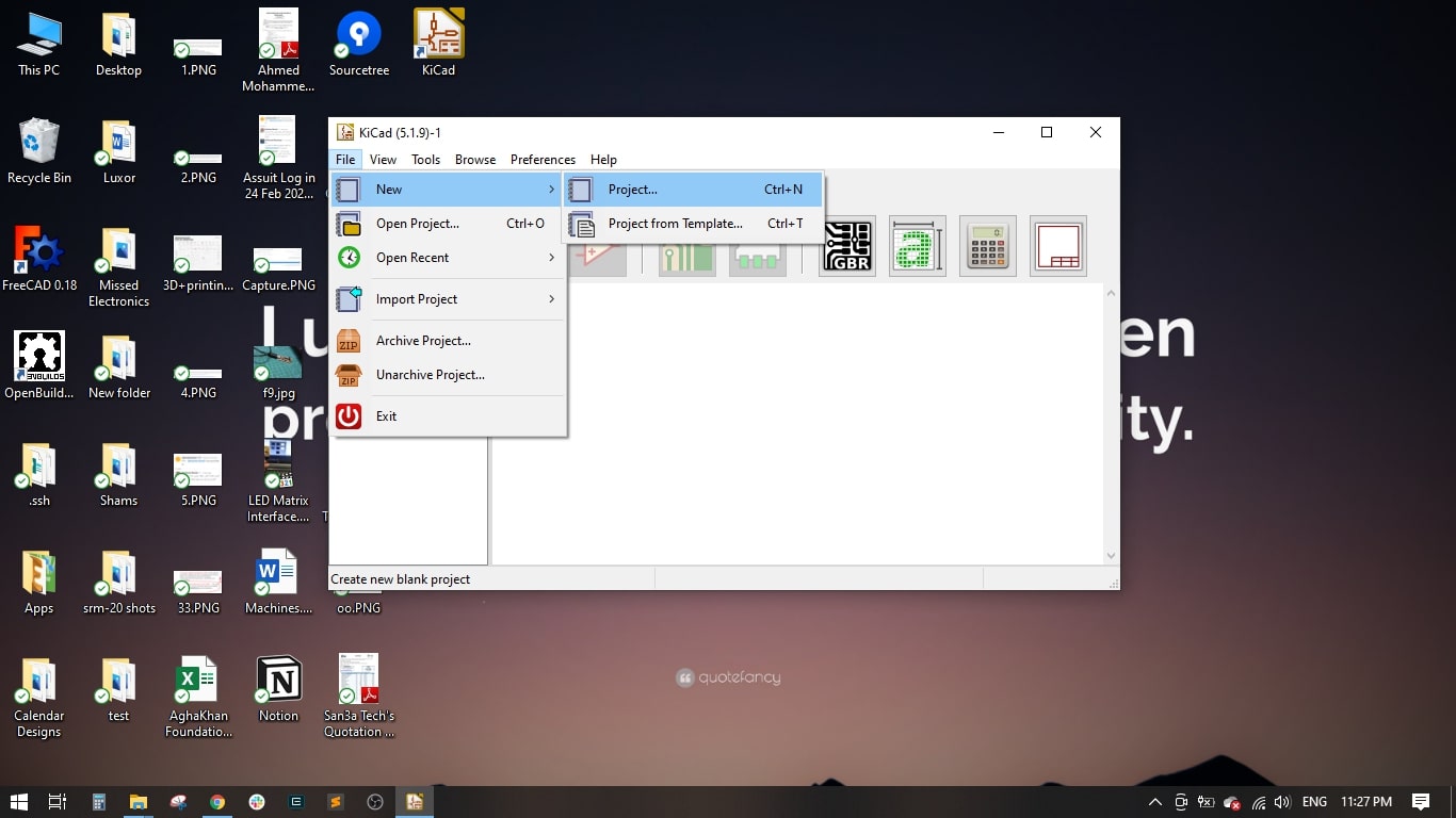
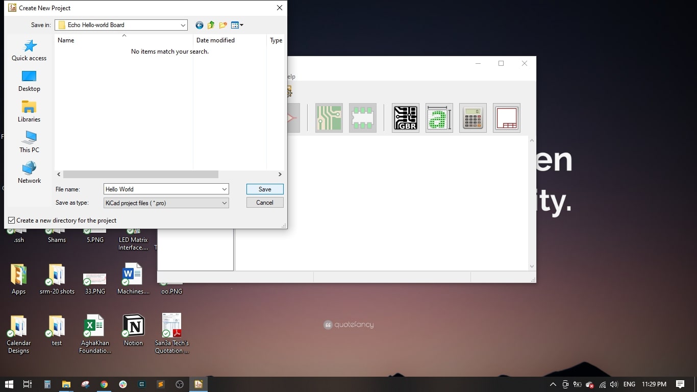
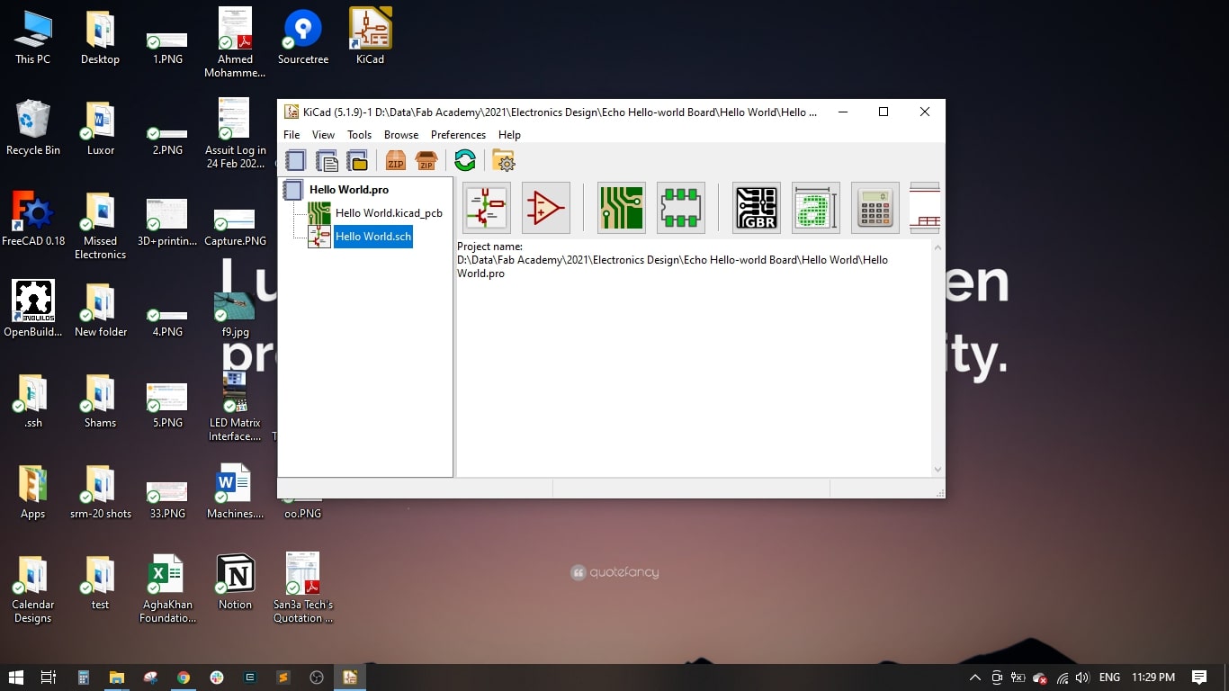
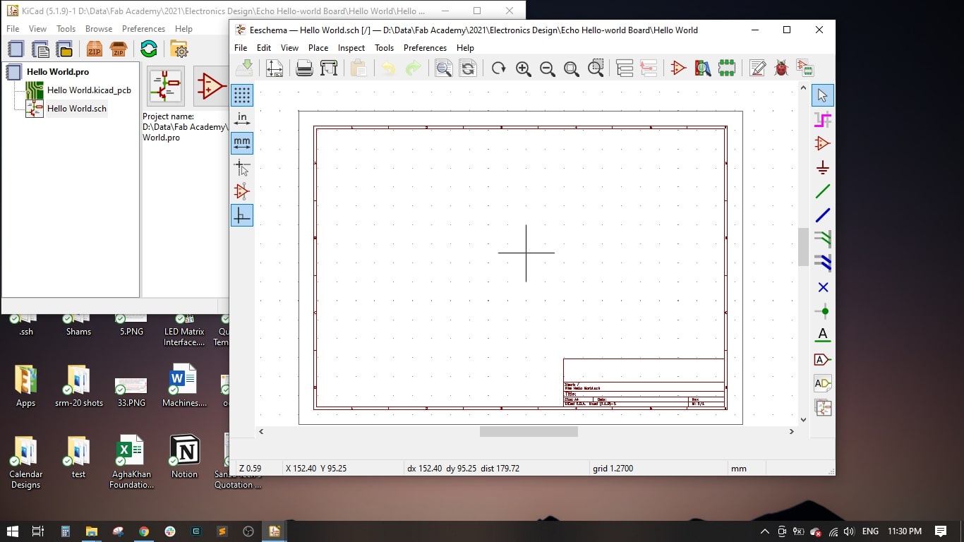
- I created a new project Hello World and opened the Schematic environment.
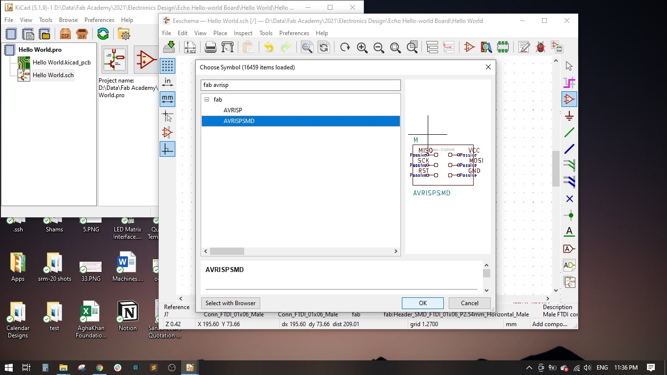
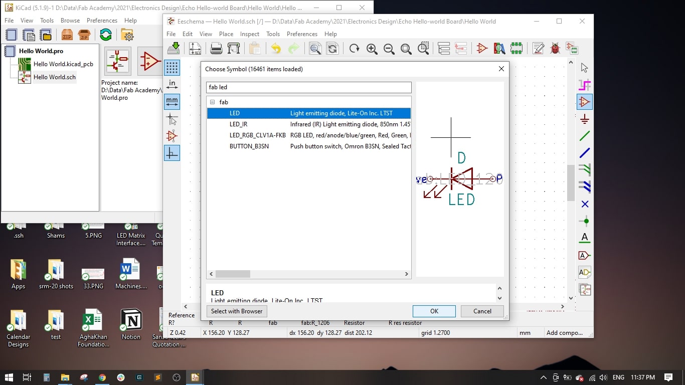
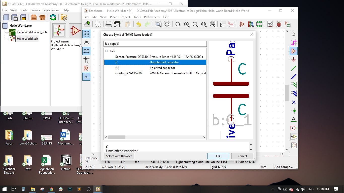
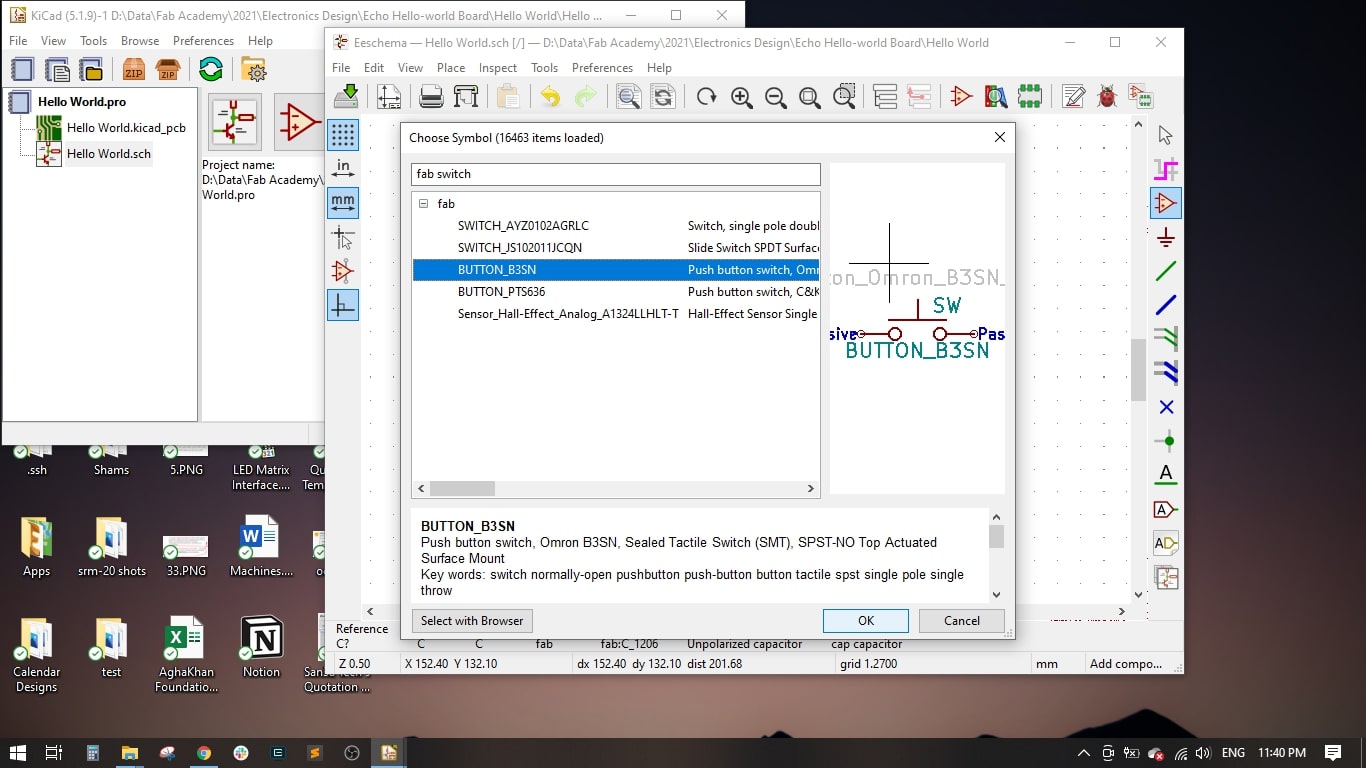
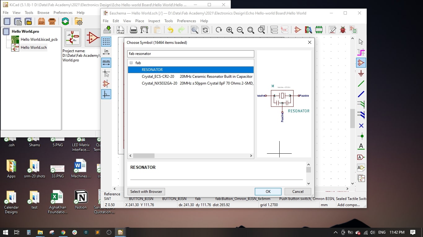
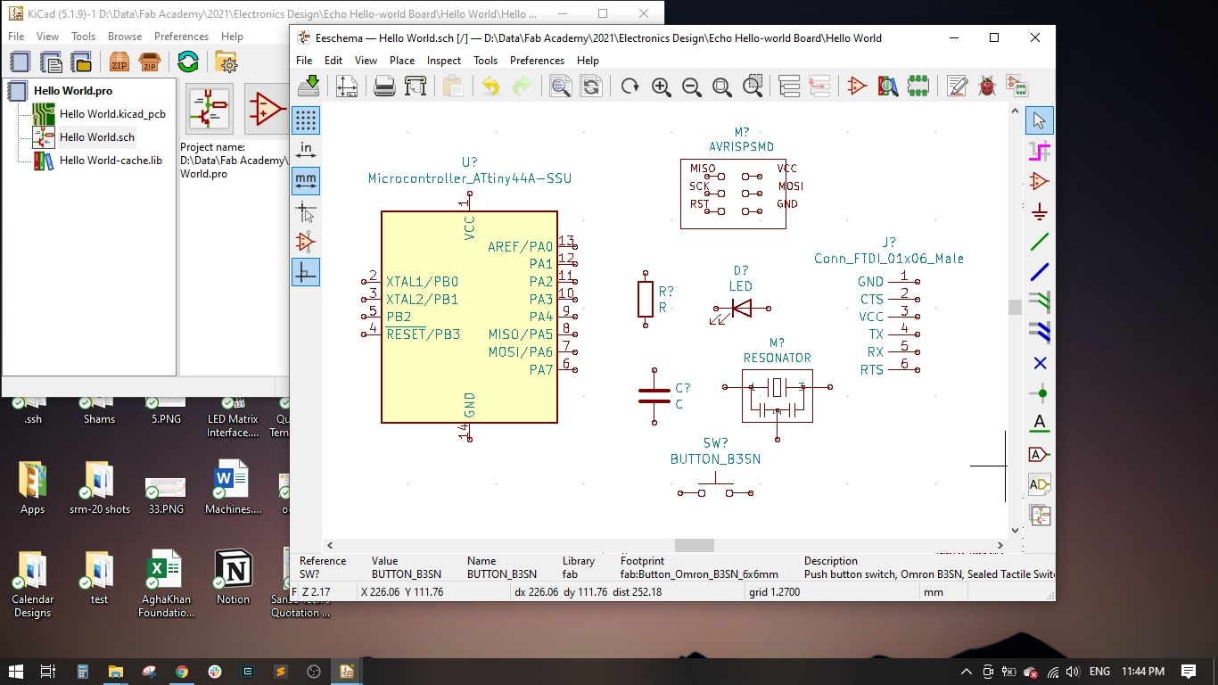
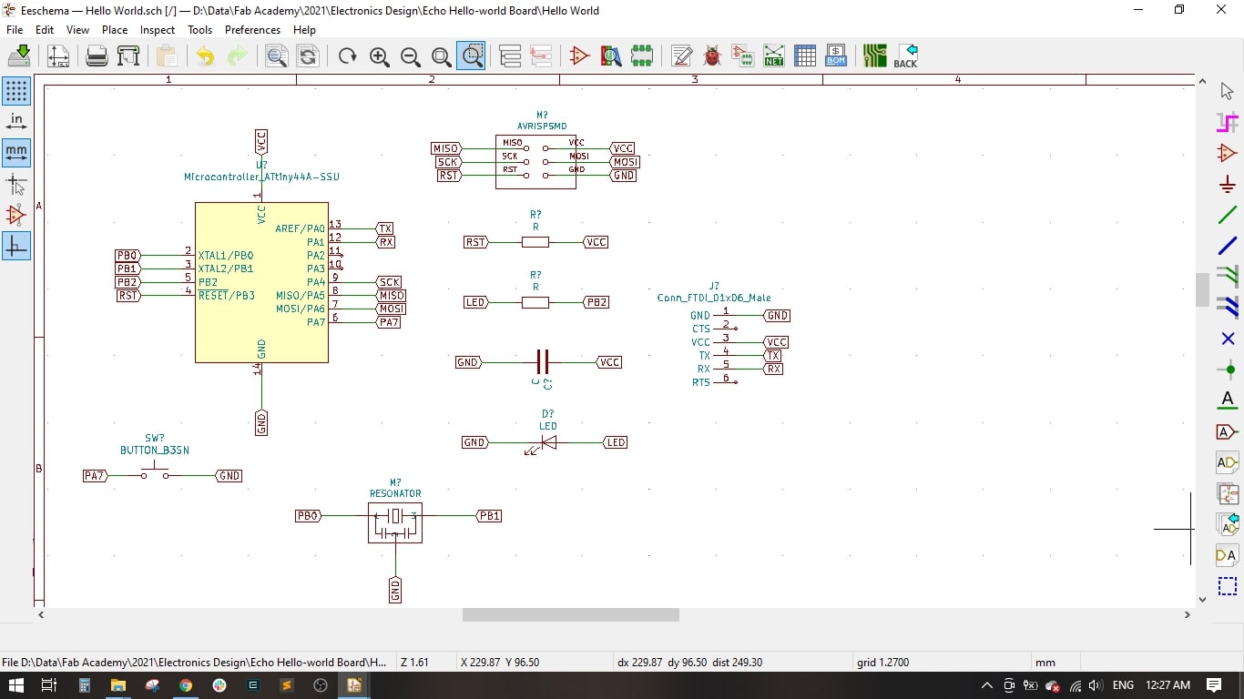
- I started adding components from the fab library
- Now I had all the required components in the schematic page and ready for wiring.
- I used the Label tool to connect each component insted of having drawn wires
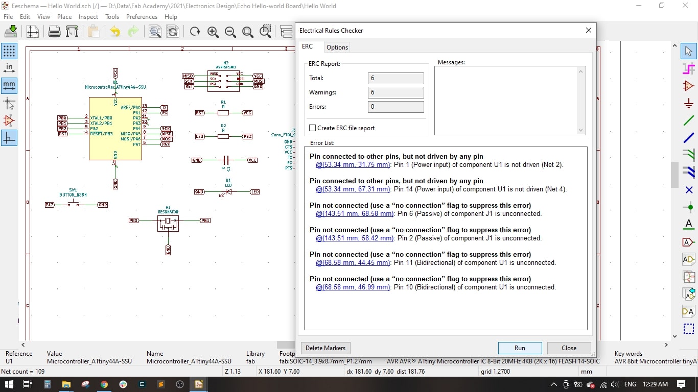
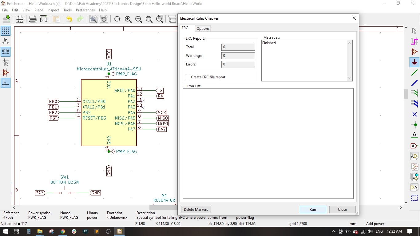
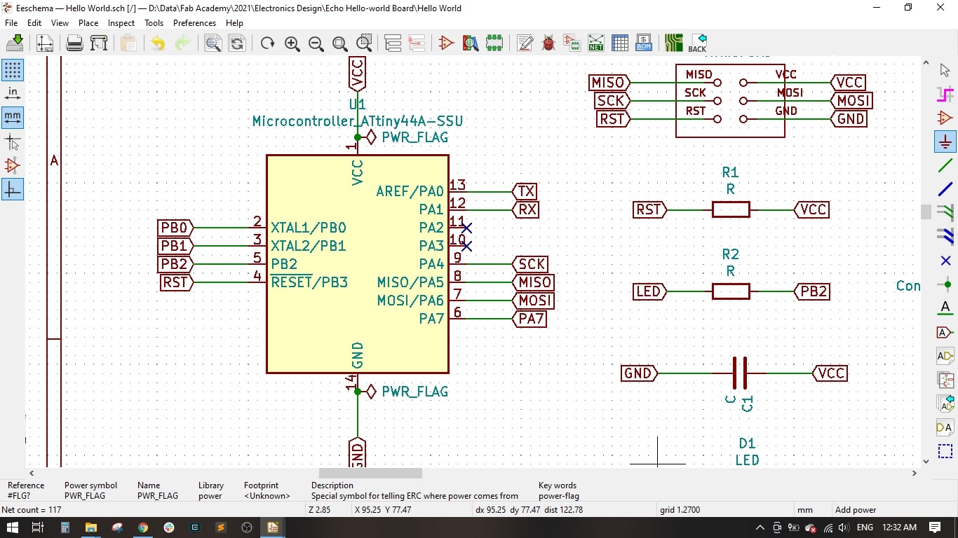
- I used the Electrical Rules Checker to check if there ia an error with the schematics and it detected some unconnected ports, so I used the Place no connection flag to mention the unused ports and the Power Flag to assign Power inputs/outputs.
- Now I finished the shematics and ready for the actual routing.
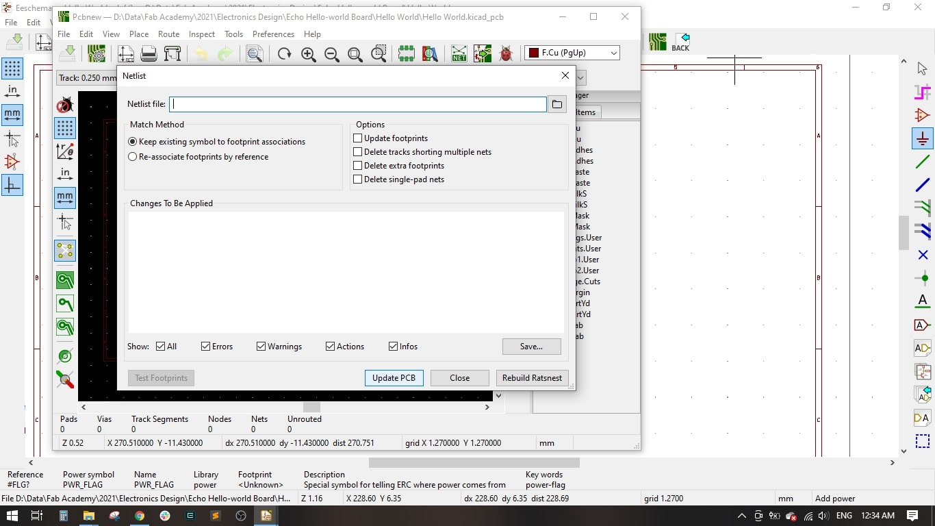
- I pressed on the Netlist and selected the Update PCB to move on the pcb routing environment.
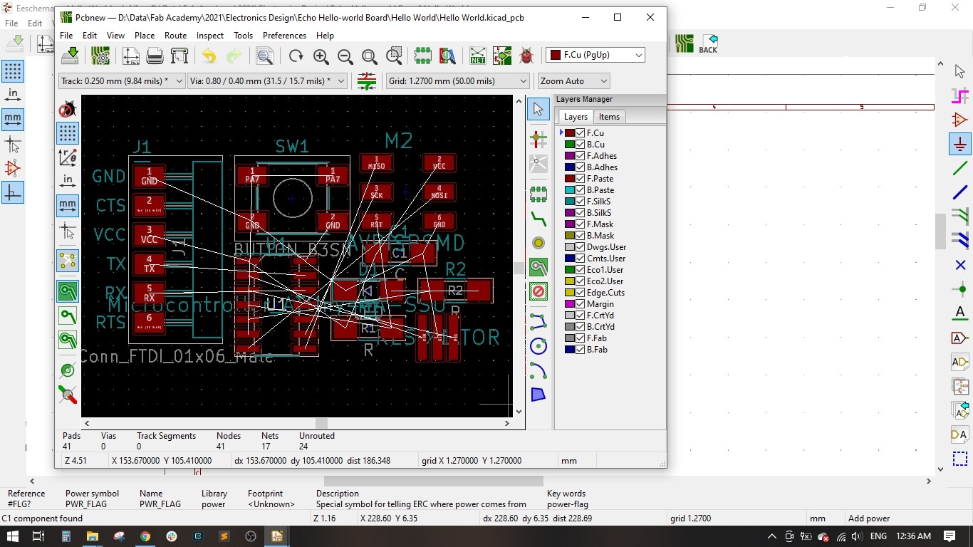
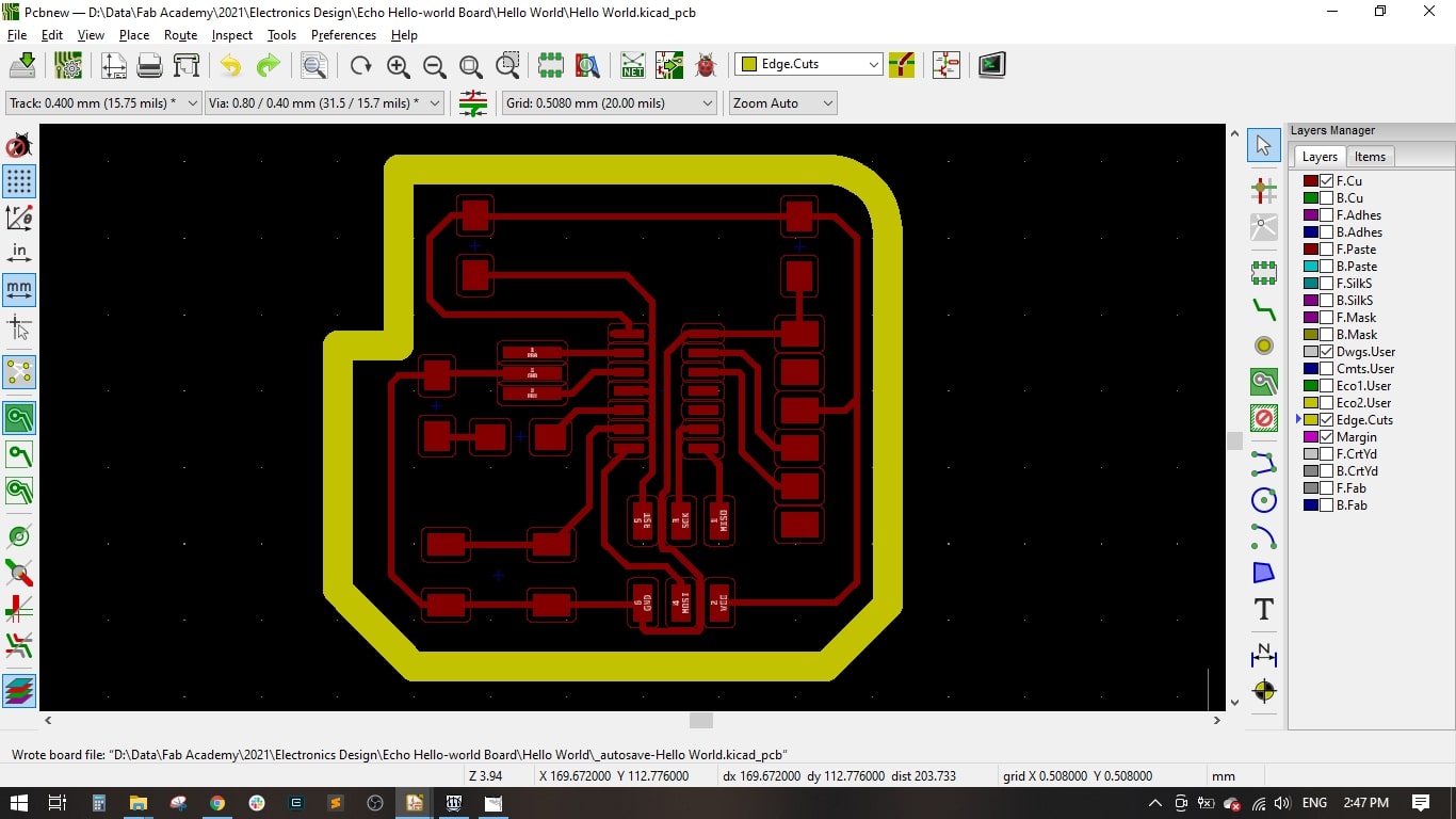
- Shown is the actual PCB that requires routing all the wires.
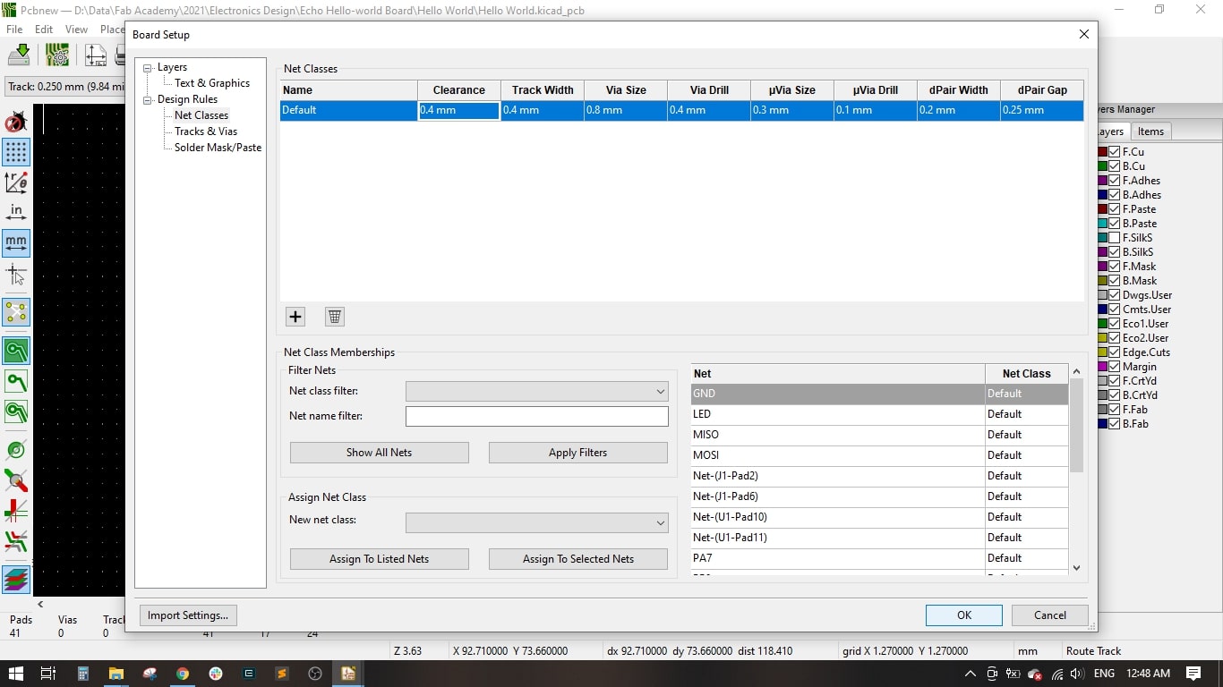
- I applied our design rules before routing, such as the track width and the clearance to 0.4 mm.
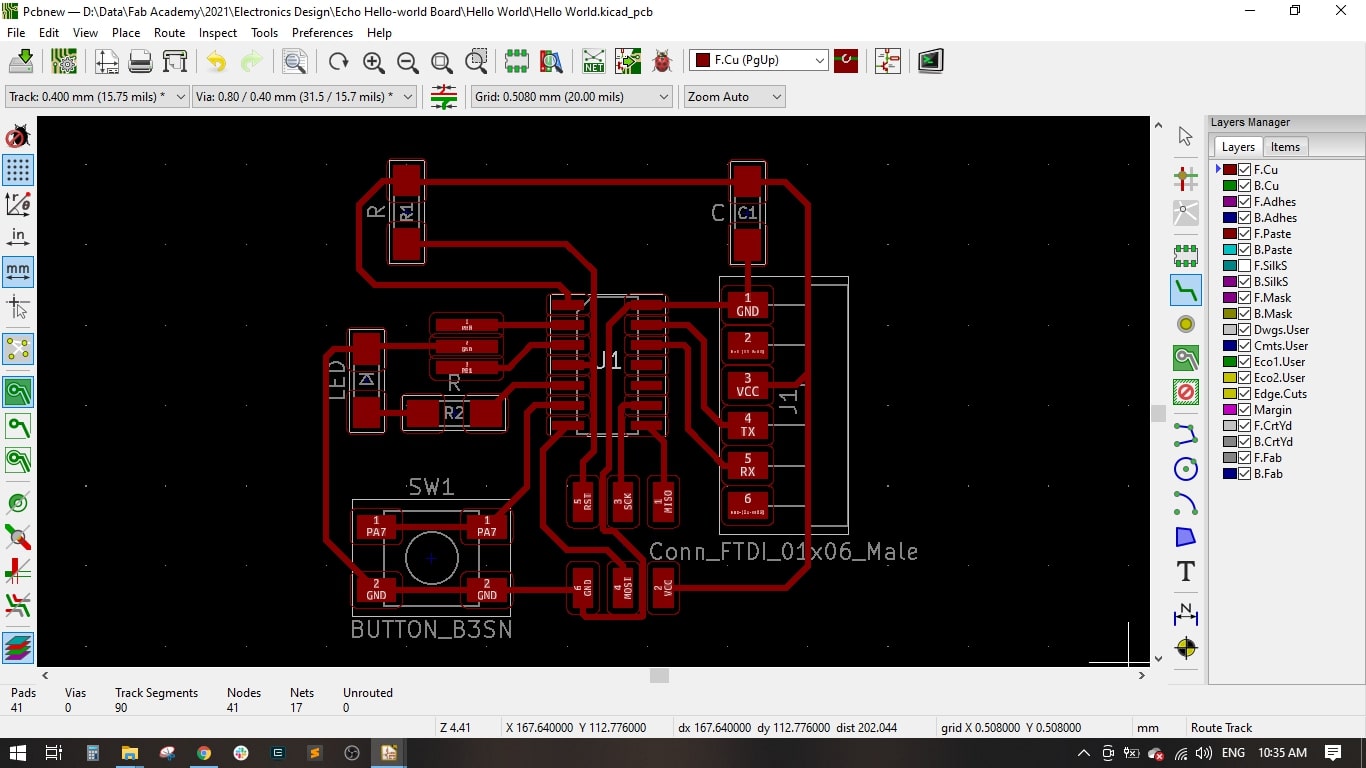
- I used the routing tool to connect all the wires anf the graphical tool to draw the board outline
- For the routing, I used 0.4 mm routes and for the outline I used a 2 mm line thickness.
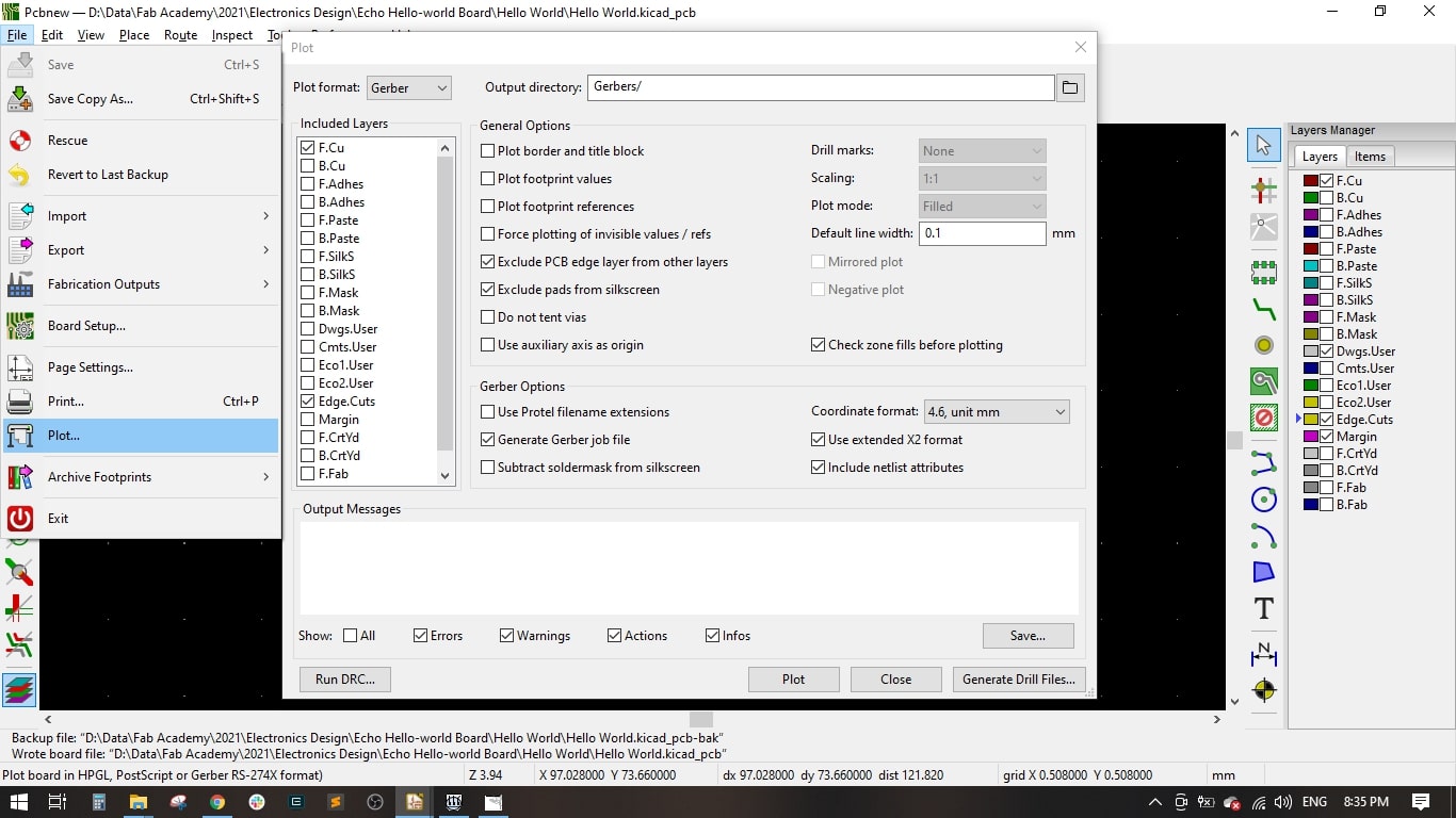
- Finally, I exported the GERBER files, I selected only the front copper layer and the edge cut layer.


Step(3): Extracting the CAM Files
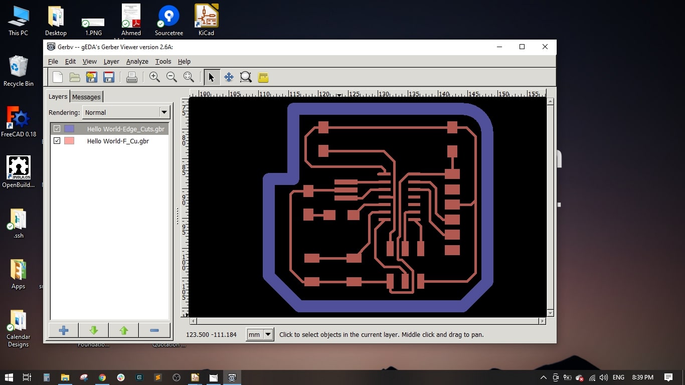
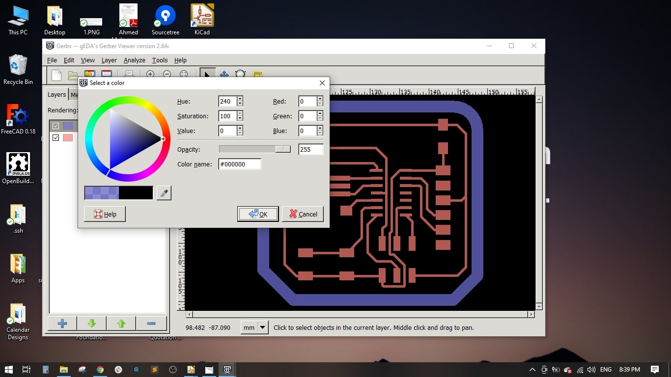
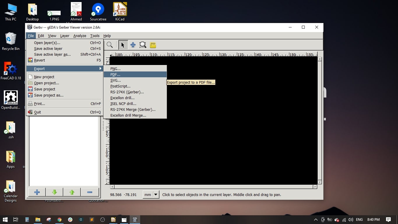
- I imported the GERBER files into Gerbv software, selected each layer and converted its layer to black.
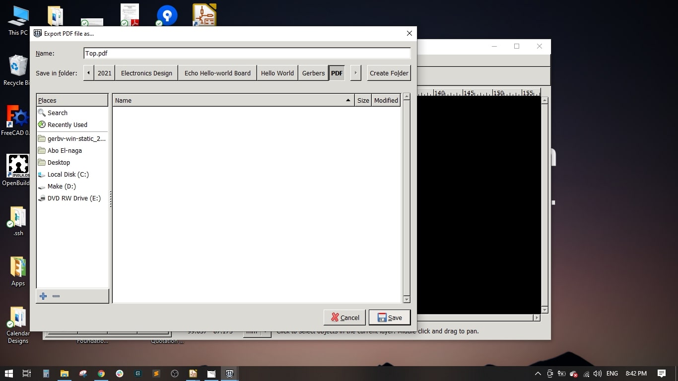
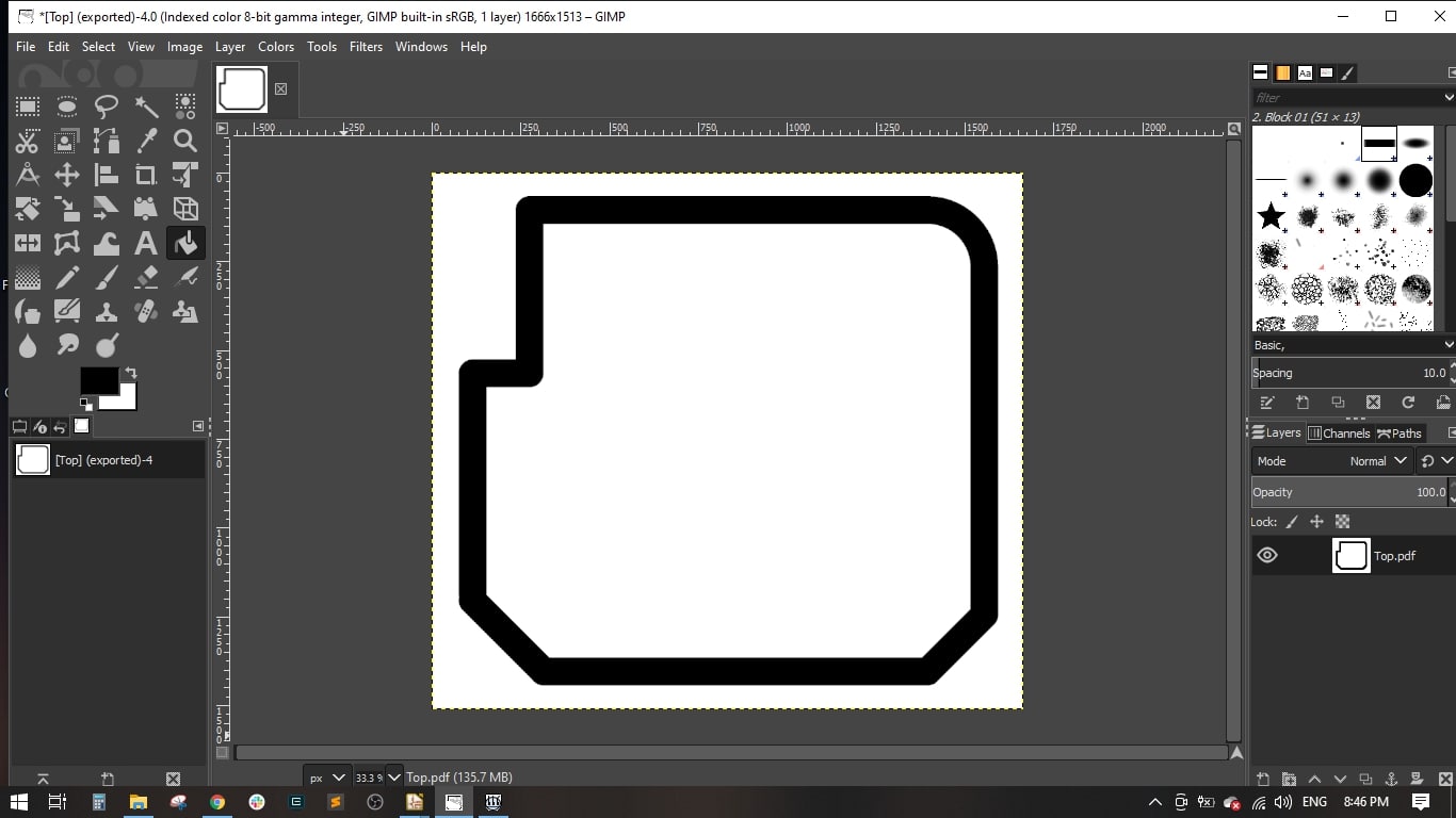
- Then, exported both layers as .pdf format
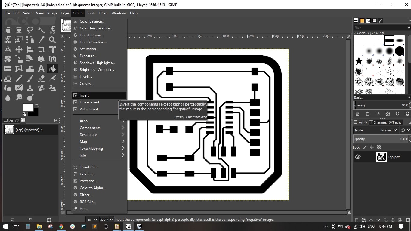
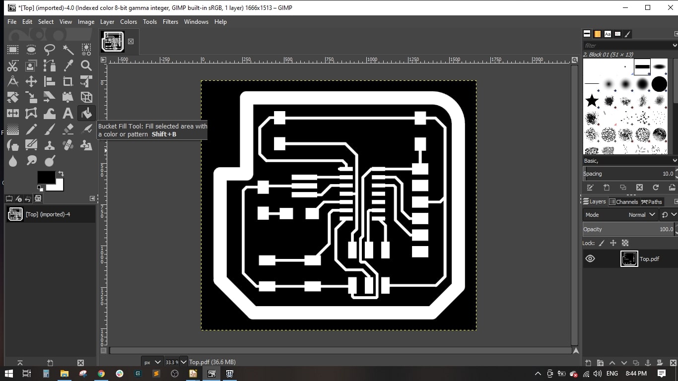
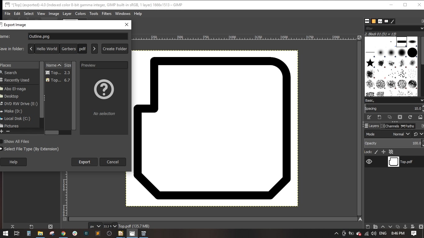
- I used GIMP to invert the colors and export the .png files, traces are in white and outline in black.
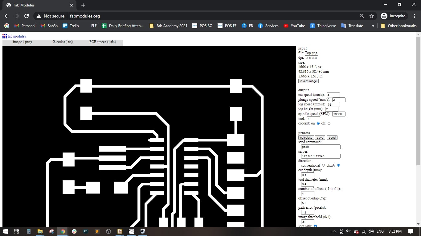
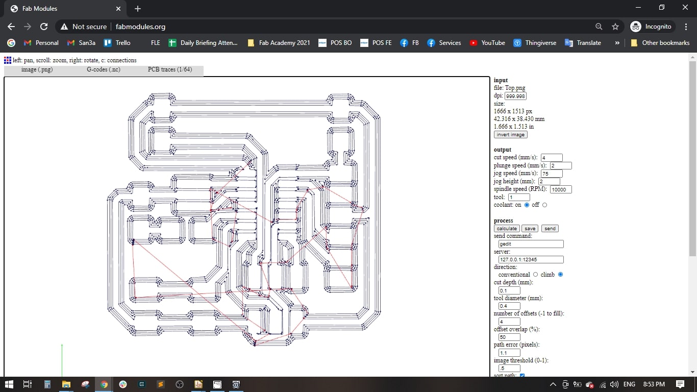
- I imported the top.png into FabModules, selected G-codes as output format and a cutting tool 1/64 inch, dpi set to 1000 as imported in GIMP, and used most of the default parameters, calculated the toolpath then saved the .gcode.
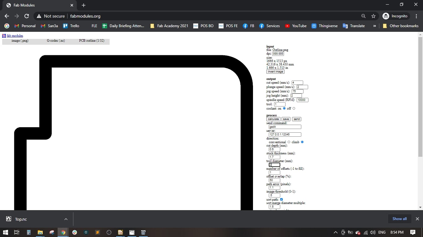
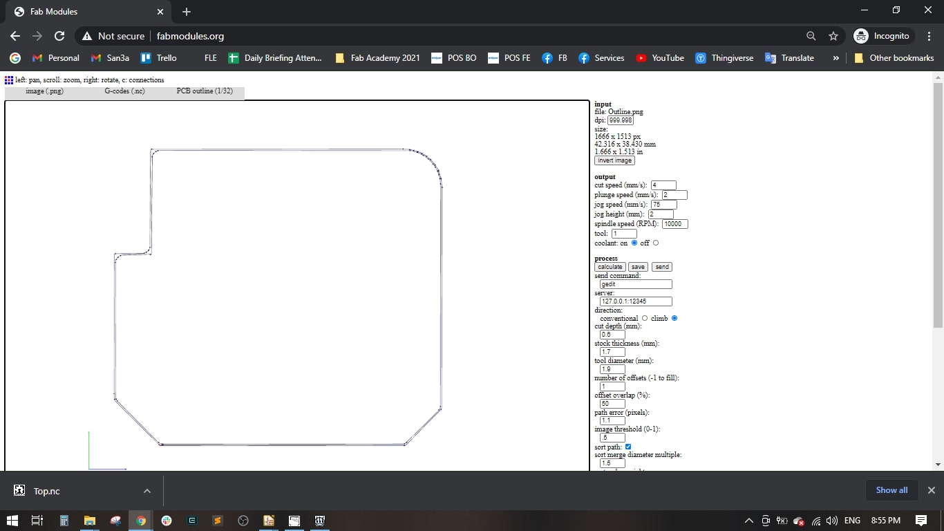
- Also imported the outline.png and selected the 1/32 endmill as cutting tool, but the actual endmill was 2 mm in diameter, calculated and saved the g-code.
Step(4): Fabricating the Board
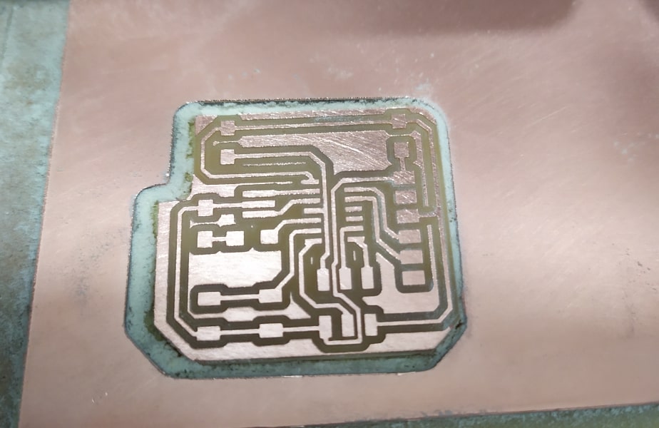
- I used the MonoFab milling machine for fabricating the board.
- First, I milled the traced using the 0.4 mm V-bit tool.
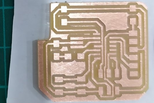
- Second, I cut the outline using an 2 mm end mill.
- And now the PCB is ready for assembly and soldering components.
Step(5): Stuffing and Soldering the Board
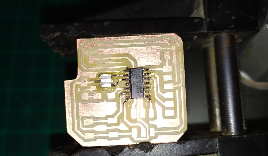
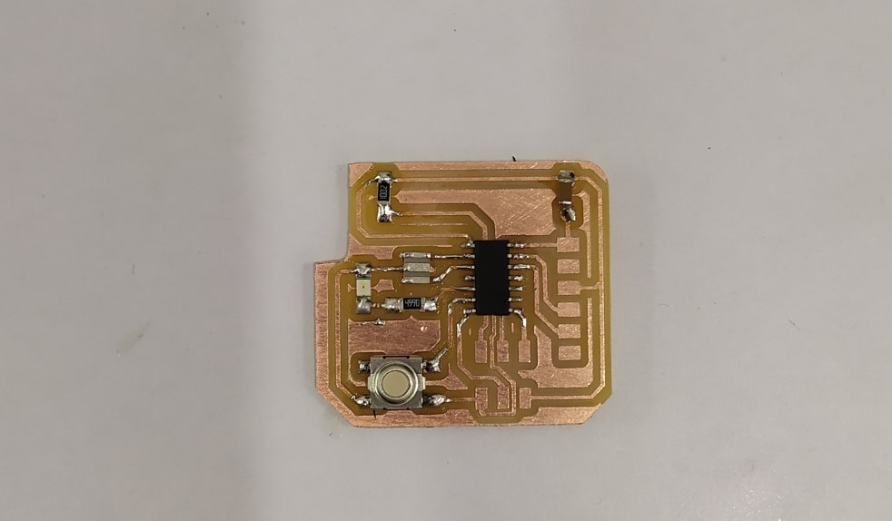
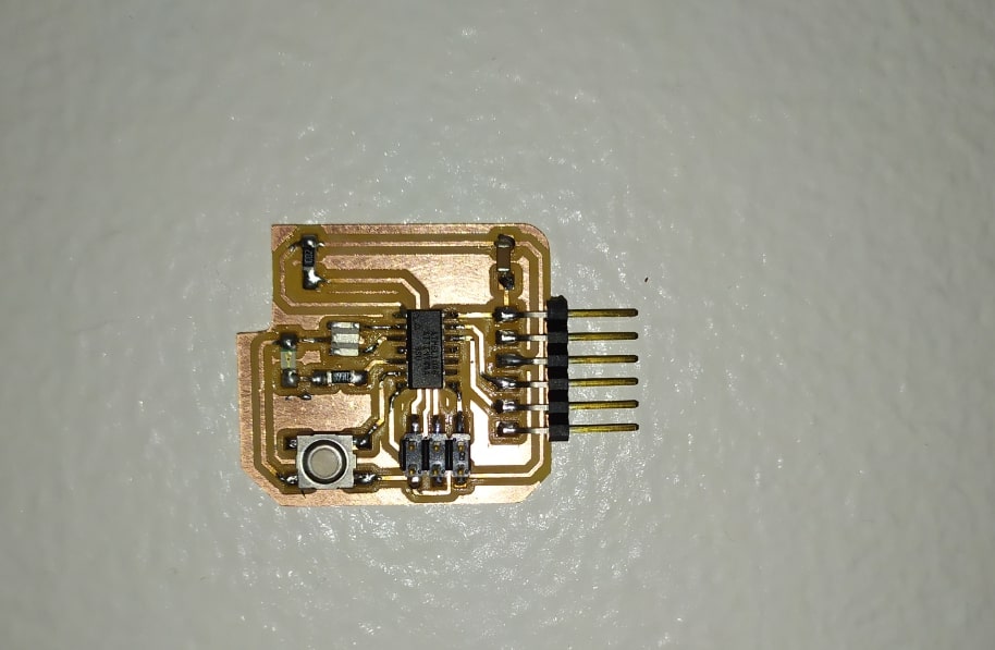
- I started with soldering the ATtiny 44 and the resonator.
- Then I soldered the resistors, capacitor, led and the push button.
- Finally, I soldered the FTDI pin header and the ISP_pin header.
Step(6): Programming & Testing
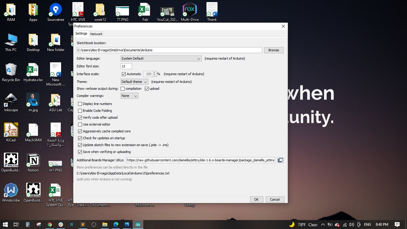
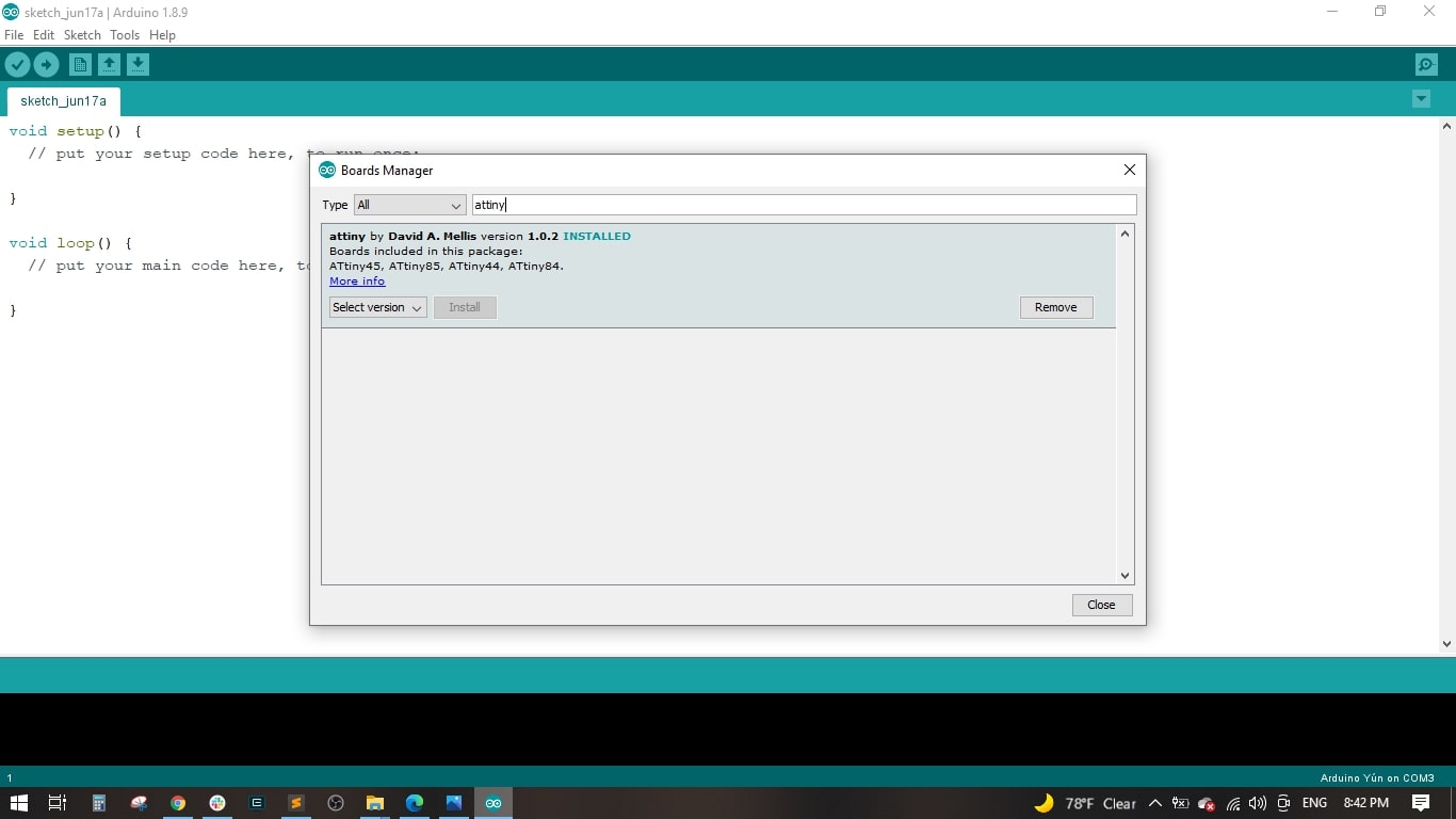
- I opened the Arduino IDE, Opened File > Preferences and pasted this URL "https://raw.githubusercontent.com/damellis/attiny/ide-1.6.x-boards-manager/package_damellis_attiny_index.json" into the Additional Boards Manager URLs and pressed OK
- Opened Tools > Board > Boards Manager and searched for attiny by David A. Mellis and installed it.
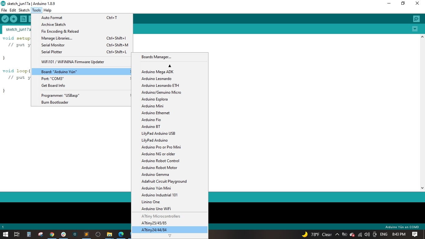
- From Tools, I selected the ATtiny 44 as the used board.
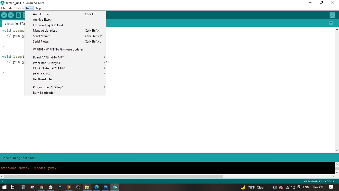
- Set the processor to ATtiny44, Clock to External 20 MHz, selected the used port, Programmer to USBasp and then Burn Bootloader
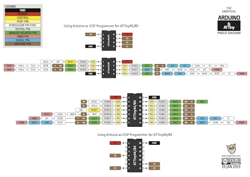
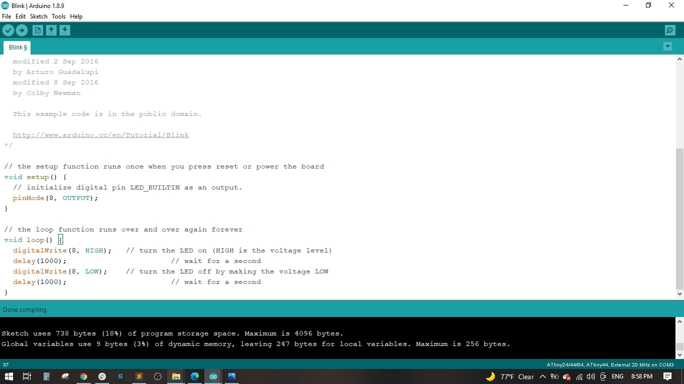
- From File > Examples > Basics > Blink, I changed the LED_BUILTIN to 8, as as the LED is connected on pin 8 and did the compiling.
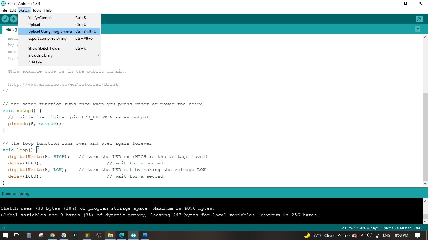
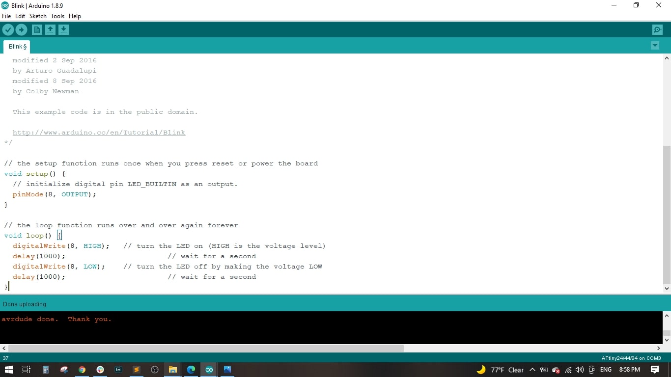
- I connected the USBasp to the laptop and connected the board to it, then I selected the port and uploaded the blink code using programmer.
- Now the code was uploaded to the board and the led is blinking each 1 sec.
Finally, I have:
√ Linked to the group assignment page.
√ Documented what I have learned in electronics design.
√ Explained problems and how I fixed them.
√ Included original design files.
√ Included a ‘hero shot’ of my board.
√ Loaded a program and tested.