Embedded Programming :-
Group Assignment
Can be found here
Individual Assignment
This week Assignment to read a microcontroller data sheet program your board to do something,with as many different programming languages and programming environments as possible.
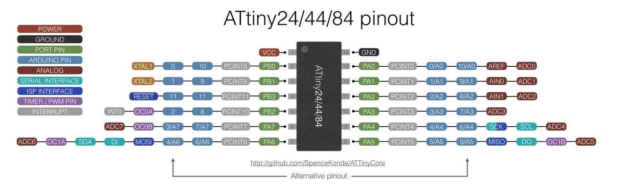
This week i first tried to read the datasheet but it is a huge document i didnot find out what to read and from where to start.First of all i went through the pin out diagram of the Atmel Attiny 44.This is an eight pin microcontroller.
Pin Description:-
| Pin | Description |
| VCC | Supply voltage. |
| GND | Ground |
| Port B (PB3...PB0) | Port B is a 4-bit bi-directional I/O port with internal pull-up resistors (selected for each bit). The Port B output buffers have symmetrical drive characteristics with both high sink and source capability except PB3, which has the RESET capability. To use pin PB3 as an I/O pin instead of RESET pin, program (‘0’) RSTDISBL fuse. As inputs, Port B pins that are externally pulled low will source current if the pull-up resistors are activated. The Port B pins are tri-stated when a reset condition becomes active, even if the clock is not running. |
| RESET | Reset input. A low level on this pin for longer than the minimum pulse length will generate a reset, even if the clock is not running. |
| Port A (PA7...PA0) | Port A is a 8-bit bi-directional I/O port with internal pull-up resistors (selected for each bit). The port A output buffers have symmetrical drive characteristics with both high sink and source capability. As inputs, Port A pins that are externally pulled low will source current if the pull-up resistors are activated. The port A pins are tri-stated when a reset condition becomes active, even if the clock is not running. |
Atmel Attiny 44 is 2 port microcontroller.
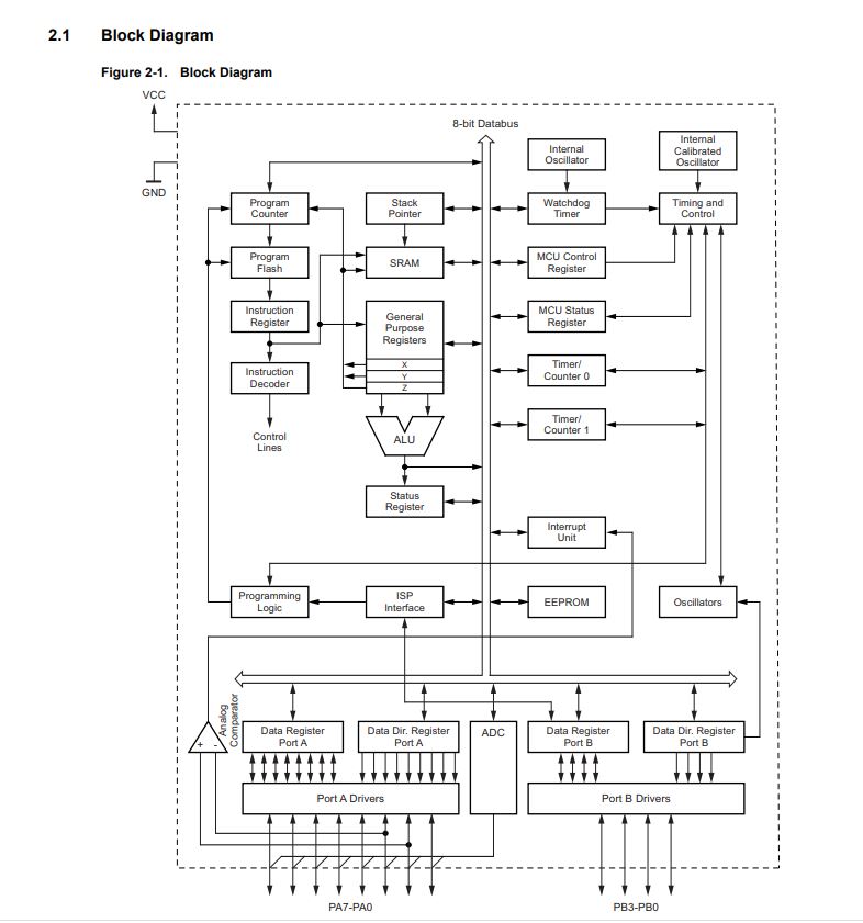
This is the block diagram of the Attiny 44 micro controller.
I followed the following tutorial
Considering the ppin configuration of Attiny 85
DDRB register:
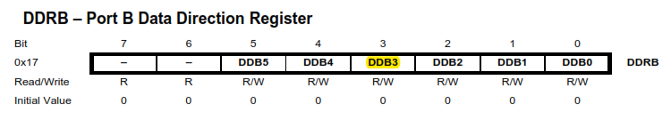
The configuration of ATtiny85 GPIO input pins starts with DDRB register, you can refer the datasheet here. We are looking to use pin 2 of attiny85 as Input. Now according to the datasheet the pin 2 is PB3 of PORTB. In order to make it as an Input we need to write the DDB3 register bit as logic ‘low’ or 0 in the code. The below piece of code will do that.
DDRB &= ~(1 << PB3);
// Set the pin PB3 as input
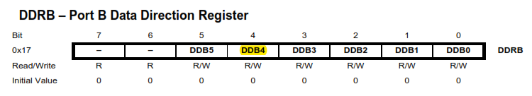
Similarly we need to define the pin 3 or PB4 as an output pin. Therefore the DDB4 register bit will be logic ‘high’ or 1.
DDRB |= (1 << PB4);
// Set the pin PB4 as output
PORTB register:
Now that we have configured the pins, we need to read the logic input from the input pin PB3. For that purpose we use PORTB register. PB3 is an Input pin, therefore we can not leave the pin floating when neither high nor low logic level are connected to it. So we need to activate the internal pull up resistor of this pin. To do that,
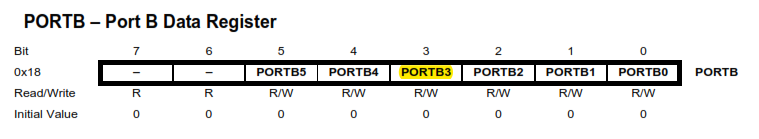
We need to set the PORTB3 register to 1. This register is generally used to set the output state of that pin high or low, but as we declare this pin as input, this will activate the internal pull up resistor.
PORTB |= (1 << PB3);
//activate pull-up resistor for PB3
Alternatively you can use an external 10k resistor to pull-up or pull-down this pin.
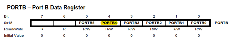
PORTB register also enables to toggle the LED state high or low. Writing ‘1’ or ‘0’ to PORTB4 toggles the LED to ON state or OFF state.
PINB register:
PINB register is where we can read the input of any pin that is configured as inpit. Here we will look for PINB3 bit value in this register without disturbing other bits.
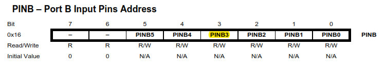
We do that using the below line
buttonState = PINB & (1 << PB3);Upon reading the input state we use this input to toggle LED ON and OFF. Like this,
if (buttonState) {
PORTB |= (1 << PB4); //write to PORTB register to set the LED state to HIGH
}
else {
PORTB &= ~(1 << PB4); //write to PORTB register to set the LED state to LOW
}
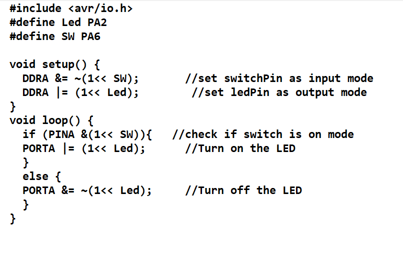
Now Considering the above programming basics i trid to understood the basics of Attiny 44
Port a has pin no PA0-PA7 and Port B has pn no PB0-PB3
and rest VCC and Gnd
for programming the Attiny 44 we use three registers
DDR - Data Directional Register
PORTx - Port Registers x= PORT A,B,C
PIN-Port Input Registers.eg PIN B,PIN D
DDR -determines the direction (I/o) of the each pin on the microcontroller.Hight at DDR register make the corresponding pin output while Low at DDR Register make the corresponding pin Input.
PORT Register-Is the output register which determines the status of each pin of a particular port.High at PORT regiuster makes corresponding pin Logic High (5V) while low at PORTx register makes Corresponding pin logic LOW (0 V) where x = 1,2,3.Genrally these registers are used to write data to ports.
PIN Registers-are used to read data from ports.
I learnt from the basic from the searching the internet about the programming in c from the following tutorial
#ifndef F_CPU
			#define F_CPU 16000000UL // 16 MHz clock speed
			#endif    #include <avr/io.h>
			#include <util/delay.h>
			int main(void)
			{    DDRC = 0xFF; //Nakes PORTC as Output
				while(1) //infinite loop
					{      PORTC = 0xFF; //Turns ON All LEDs
					_delay_ms(1000); //1 second delay
					PORTC= 0x00; //Turns OFF All LEDs
					_delay_ms(1000); //1 second delay
					}
			}
- DDRC = 0xFF makes all pins on PORTC as output pins
- PORTC = 0xFF makes all pins on PORTC Logic High (5V)
- PORTC = 0x00 makes all pins on PORTC Logic Low (0V)
- _delay_ms(1000) provides 1000 milliseconds delay.
- while(1) makes an infinite loop
You have seen that PORT registers are used to write data to ports. Similarly to read data from ports PIN registers are used. It stand for Port Input Register. eg : PIND, PINB
You may like to set or reset individual pins of PORT or DDR registers or to know the status of a specific bit of PIN register. There registers are not bit addressable, so we can’t do it directly but we can do it through program. To make 3ed bit (PC2) of DDRC register low we can use DDRC &= ~(1<<PC2). (1<<PC2) generates the binary number 00000100, which is complemented 11111011 and ANDed with DDRC register, which makes the 3ed bit 0. Similarly DDRC |= (1<<PC2) can be used set the 3ed bit (PC2) of DDRC register and to read 3ed bit (PC2) we can use PINC & (1<<PC2). Similarly we can set or reset each bit of DDR or PORT registers and able to know the logic state of a particular bit of PIN register.
I undergone throu some more tutorials here and here
Atmel Studio C Program
#ifndef F_CPU
#define F_CPU 16000000UL // 16 MHz clock speed
#endif    #include <avr/io.h>  #include <util/delay.h>
int main(void)
{    DDRC = 0xFF; //Nakes PORTC as Output
while(1) //infinite loop
	{      PORTC = 0xFF; //Turns ON All LEDs
	_delay_ms(1000); //1 second delay
	PORTC= 0x00; //Turns OFF All LEDs
	_delay_ms(1000); //1 second delay
	}
 }
- DDRC = 0xFF makes all pins on PORTC as output pins
- PORTC = 0xFF makes all pins on PORTC Logic High (5V)
- PORTC = 0x00 makes all pins on PORTC Logic Low (0V)
- _delay_ms(1000) provides 1000 milliseconds delay.
- while(1) makes an infinite loop
You have seen that PORT registers are used to write data to ports. Similarly to read data from ports PIN registers are used. It stand for Port Input Register. eg : PIND, PINB
You may like to set or reset individual pins of PORT or DDR registers or to know the status of a specific bit of PIN register. There registers are not bit addressable, so we can’t do it directly but we can do it through program. To make 3ed bit (PC2) of DDRC register low we can use DDRC &= ~(1<<PC2). (1<<PC2) generates the binary number 00000100, which is complemented 11111011 and ANDed with DDRC register, which makes the 3ed bit 0. Similarly DDRC |= (1<<PC2) can be used set the 3ed bit (PC2) of DDRC register and to read 3ed bit (PC2) we can use PINC & (1<<PC2). Similarly we can set or reset each bit of DDR or PORT registers and able to know the logic state of a particular bit of PIN register.
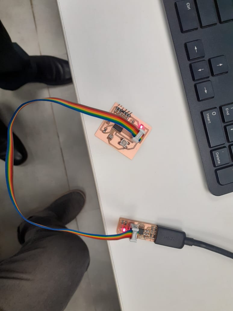
This week i had to programm the board which i had made in the Electronics Design Week using Ardiuno IDE.
Ardiuno IDE -The Arduino Integrated Development Environment - or Arduino Software (IDE) - contains a text editor for writing code, a message area, a text console, a toolbar with buttons for common functions and a series of menus. It connects to the Arduino and Genuino hardware to upload programs and communicate with them.
I circuit diagram of the board whic i make is 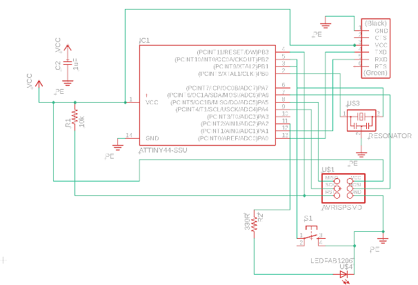
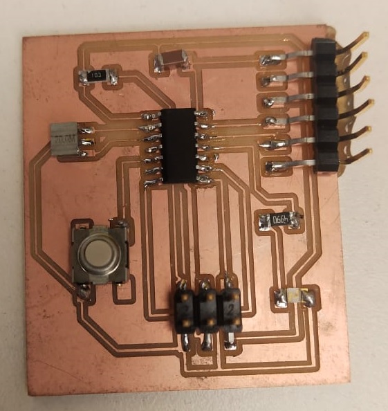
I Soldered the board with the required components accordingly
First of all in arduino IDE i Had to add ATtiny 44 Board to program my board:
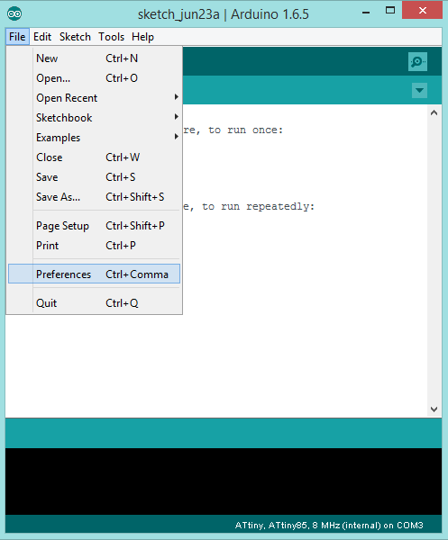
Open Ardiuno IDE click File-> Prefrences
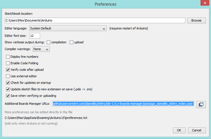
URL to add to the ‘Additional Boards Manager URLs’ field: https://raw.githubusercontent.com/damellis/attiny/ide-1.6.x-boards-manager/package_damellis_attiny_index.json
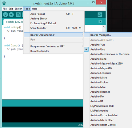
- After adding the URL open Board Manager by clicking Tools >> Board >> Board Manager
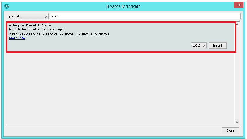
-Search for ATtiny44 in the following Window.(Make sure you have Internet connection).and Install the latest version .
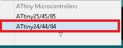
- Now you can select ATtiny44 under the ATtiny Microcontrollers in board Selection
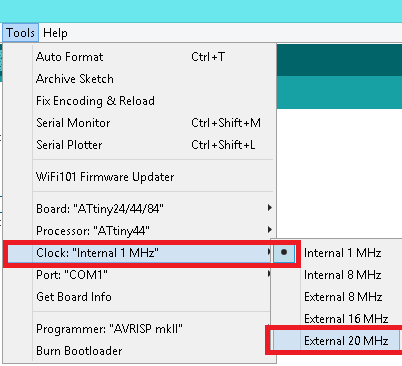
- Select the Clock as 20MHz.
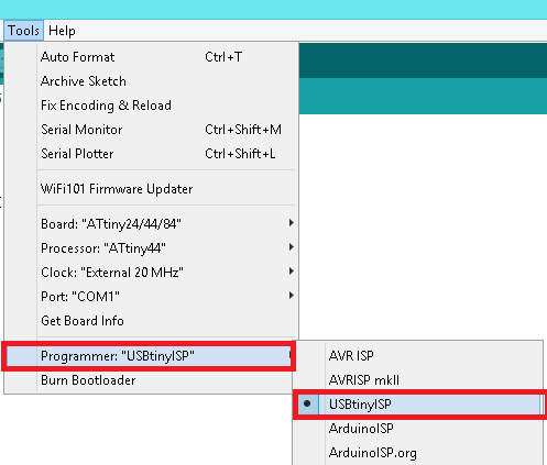
We are using Fab ISP to programme the Hello-Echo board, so Select the Programmer as USBtinyISP.
Now Write the code in the in the ardiuno IDE
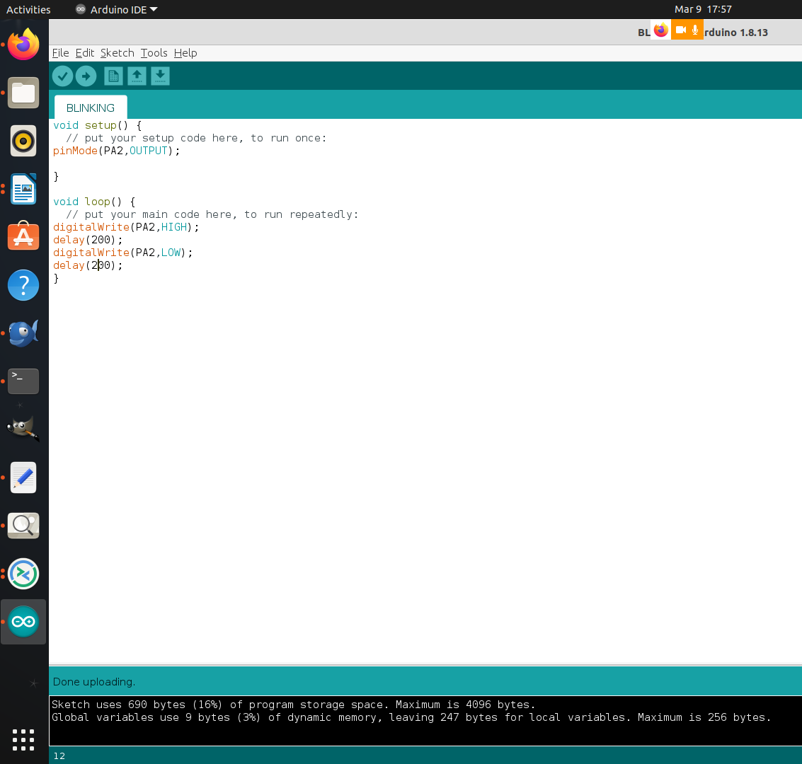
I was not aqainted wth the arduino programming i took the help of the instructor Mr.Sheebu.Who helped me in programming the pcb.
Blinking LED
void setup() {#define LED 8#define SW 7void setup(){pinMode(LED, OUTPUT);pinMode(SW, INPUT);}void loop(){digitalWrite(LED, HIGH);delay(1000);digitalWrite(LED, LOW);delay(1000);}
Toggle
#define LED PA2#define SW PA6// toggle the led status upon button pressboolean prev_btn_stat=HIGH;boolean prev_led_stat=LOW;boolean current_btn_stat;void setup() {// put your setup code here, to run once:pinMode(LED,OUTPUT);digitalWrite(LED,LOW);pinMode(SW,INPUT_PULLUP);}void loop(){prev_btn_stat = current_btn_stat;current_btn_stat = digitalRead(SW);if(!current_btn_stat && (current_btn_stat != prev_btn_stat) ){delay(5); //debouncing with 1ms delayif ( prev_led_stat ){digitalWrite(LED,LOW);prev_led_stat = LOW;}else{digitalWrite(LED,HIGH);prev_led_stat = HIGH;}}delay(200);}
LED PULL UP
const int ledPin = 7;int BUTTONState = 0;void setup(){pinMode(PA2, OUTPUT);pinMode(PB2, INPUT_PULLUP);}void loop(){BUTTONState = digitalRead(PB1);if (BUTTONState == 0){digitalWrite(PA2, LOW);}else{digitalWrite(PA2, HIGH);}}
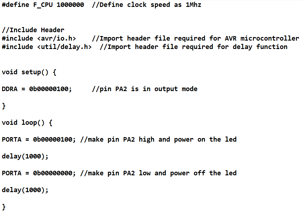
In this assignment week faced the problem in programming.I had to go through lot of good tutorials and i also made the personal notes in the notebook regarding the programming in c.I have also done the programming using the register programming.
Blink LED
Blink LED 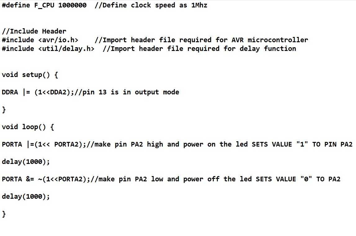
Button LED