7. Electronics design
The assignment for this week is centered around PCB design. More specifically, I should demonstrate the use of electronics components as part of a functional circuit.
I decided to build 3 different projects:
- a small board based on a D11C that shows the use of LED, an optical switch and a physical switch.
- a combined UPDI/UART programmer, also based on a D11C.
- a generic controller board based on the ATtiny1614
For each board, I focus on different design methods. In our group assignment, we tested the oscilloscope to get familiar with debugging circuits.
D11C optical endstop (EAGLE)
I am already familiar with EAGLE but haven’t used it in a while. I wanted to create the most compact board that could demonstrate the use of basic components. I found an old optical endstop at the lab. I add some resistors: one of them limits the current going into the IR LED, while the other one acts as a pull-up when the photo-diode is blocking.
I make sure to connect this the anode of the photo-diode to an analog pin of the D11C. This way, I can adjust the threshold in software, to make the endstop more or less sensitive to a blocking of the IR light.
On the schematic, I also add:
- a JTAG connector for programming
- a tactile switch with a pull-up resistor
- some debug LED connected to a GPIO pin of the D11C

I can then switch to the board design. EAGLE indicates all non-connected wires in yellow, called airwires. They should either be routed manually, or auto-routed. It should be noted that these wires always indicate the closest pad, which is not necessarily the best solution if you move the devices. In that case, the airwires should be updated using the ratsnest option on the left.

After moving hte components around, I realized I had no choice but to use the tactile switch as a jumper. This is not the best practice, as there might not be any guarantee on the current that can flow through these pins, but for my application I decided to proceed this way. This keeps my board at a minimal size, however EAGLE will not marked this connection as solved, as these pins are not 100% equivalent in terms of schematic. I tried to short them in the schematic, but this would not solve the issue, so I decided to simply ignore the warning from EAGLE.

After adding a ground plane, I check that there is no airwire remaining, except the ones mentioned earlier. I also run the DRC to check that a clearance of 1/64” is present on the whole board.

As the Bantam tools software is compatible with EAGLE files, I simply load the .brd file and set the right tool. I first use the 1/64” tool for the fine details:

Then I finish with a 1mm flat end mill for the rough details and the edge:

Milling took about 20 minutes, both jobs included.

Stuffing the board was a bit tricky because of its small size. I started with the extremely thin pins of the Mini-USB connector, then worked my way outwards starting with the D11C in the middle.

The finished board includes the plastic casing from the optical endstop. I intially wanted to remove it to save some space, but it helps protecting the two IR LEDs. To include it, I had to make some compromise on the solder joint position for the IR emitter diode.

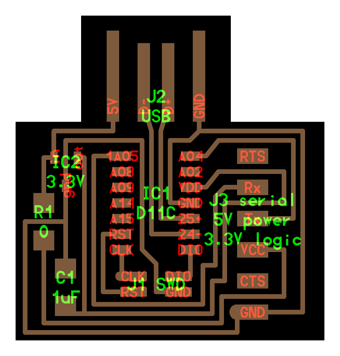
D11C UPDI/UART programmer (EAGLE/Python)
EAGLE design
When programming a UPDI board, a simple UART programmer can be used, as long as a resistor is appropriately placed between the RX and TX pins. This is a nice trick that turns the full-duplex UART into a half-duplex channel, where the same signal is available on both pins. This also means that any data sent on the TX pin is directly echoed back to the RX pin, which should be taken into account when using the port.
For this side-project, I want to improve the D11C serial programmer to add an optional UPDI output, enabled through a jumper connector. Additionally another jumper should let the user set the target VCC to either 3.3V or 5V.
When programming a 5V target chip, a 3.3V logic can still be used thanks to the pretty high tolerance of the serial protocol. However, the response from the target will be 5V anyhow, so we should protect the RX pin on our D11C board. This is done with the addition of a Zener diode and a small resistor to limit the current pulled from the target’s output pin.
I started by drawing a schematic in EAGLE.

I quickly prototype the routing in EAGLE, even if my final design will be done in a different way.

My design seemed very compact so I printed a black/white version on paper to check if all components would fit. The result was OK.

Here again, I first mill the board with a 1/64” tool, then finish it with a 1mm tool.

I can safely ignore the areas marked in red, as they have already been milled during the 1/64” pass.

The result was milled in less than 25 minutes thanks to the use of two different flat end mills.

Stuffing the board was not too tricky. This time, I did not want to waste space with a 5x2 pins JTAG connector for programming the D11C, so I went for a more compact 2x2 connector.

The final board includes a full-sized UART and UPDI connector. When using the UPDI connector, the jumper pins next to it should be shorted to enable the RX/TX resistor.
At the time of writing, programming and using the board is still experimental. In the following picture, you may notice I temporarily disconnected the Zener diode; I will connect it back once I am confident the UART is functional.

For programming the board, I start by downlading the sam_ba_Generic_D11C14A_SAMD11C14A.bin bootloader, as well as edbg to load the binary on the board. When programming the D11C, you have to find a way to connect a JTAG programmer to the 2x2 pin conenctor on the pcb. As the JTAG programmer I have here only supports 1.27mm pitch connectors, I insert individual wires:

When programming the board, it is important to provide a power supply, as my connector ignores the VCC. I use a USB hub to provide power to both devices simultaneously.

I open a terminal and run the following command to flash the device:
edbg -bpv -e -t samd11 -f sam_ba_Generic_D11C14A_SAMD11C14A.bin
Pay attention to the -e parameter, which tells edbg to completely erase the memory before starting. This makes sure any previously installed bootloader gets removed. The output of the command should look like this:
Debugger: ARM CMSIS-DAP 1093000031387d241239333437353533a5a5a5a597969906 1.10 (S)
Clock frequency: 16.0 MHz
Target: SAM D11C14A (Rev B)
Erasing...  done.
Programming................... done.
Verification................... done.
The board is now ready to use together with the Arduino software: it should appear as a serial port with the name “MattairTech Xeno Mini”.

Python design
After checking that the board could be easily produced, I started re-drawing it using the pcb.py method developed by prof. Gershenfeld. This is a standalone Python script that can produce the desirede PCB board after specifying the position of each component and the wires connecting them.
The interesting aspect is that the script actually produces a string: it describes the shapes through a set of boolean operations. For instance, a circle of radius 2 would be described as:
x*x + y*y < 2*2
This string can then be rasterized and turned into a .png file by frep.py. I found that the text editor Atom allows me to simultaneously edit the Python code, run it through a terminal and visualize the result. I particularly enjoy the image viewer, as it automatically refreshes the file, and it does not apply any filtering when inceasing the picture size: I can see each pixel as it is.

Placing the components on the board was not an issue, but I found that the wiring is sometimes a bit tedious. To make it faster, I propose to add chamfer wires as a new feature. Basically, it is equivalent to a point, but a chamfer size is specified through the dist parameter. Optionnally, a dist2 can be specified to have a non-symetrical chamfer:
class chamfer:
    def __init__(self,x,y,z=0,dist=0.01,dist2=None):
        self.x = x
        self.y = y
        self.z = z
        self.dist1 = dist
        if dist2 is None:
            self.dist2 = dist
        else:
            self.dist2 = dist2
I modified the wire() function so that if a chamfer object is detected, the displacements towards the previous and next point are computed and the chamfer is created as 2 points instead of just 1.
def wire(pcb,width,*points):
    x0 = points[0].x
    y0 = points[0].y
    z0 = points[0].z
    pcb.board = add(pcb.board,cylinder(x0,y0,z0,z0,width/2))
    for i in range(1,len(points)):
        x1 = points[i].x
        y1 = points[i].y
        z1 = points[i].z
        if isinstance(points[i], chamfer) and i < len(points)-1:
            x2 = points[i+1].x
            y2 = points[i+1].y
            z2 = points[i+1].z
            v0=(x0-x1,y0-y1)
            v2=(x2-x1,y2-y1)
            len0 = math.sqrt(v0[0]*v0[0]+v0[1]*v0[1])
            len2 = math.sqrt(v2[0]*v2[0]+v2[1]*v2[1])
            if len0 == 0 or len2 == 0:
                raise RuntimeError("Cannot create chamfer on 0 length wire")
            d0 = points[i].dist1
            d2 = points[i].dist2
            x1_0, y1_0 = (x1+d0*v0[0]/len0,y1+d0*v0[1]/len0)
            x1_2, y1_2 = (x1+d2*v2[0]/len2,y1+d2*v2[1]/len2)
            pcb.board = add(pcb.board,line(x0,y0,x1_0,y1_0,z1,width))
            pcb.board = add(pcb.board,cylinder(x1_0,y1_0,z1,z1,width/2))
            pcb.board = add(pcb.board,line(x1_0,y1_0,x1_2,y1_2,z1,width))
            pcb.board = add(pcb.board,cylinder(x1_2,y1_2,z1,z1,width/2))
            x0 = x1_2
            y0 = y1_2
            z0 = z1
        else:
            pcb.board = add(pcb.board,line(x0,y0,x1,y1,z1,width))
            pcb.board = add(pcb.board,cylinder(x1,y1,z1,z1,width/2))
            x0 = x1
            y0 = y1
            z0 = z1
    return pcb
The following example shows that you can easily mix points and chamfer on the same wire.

It took a few hours to manually translate my design into this Python script format. If you want to test it yourself or use the proposed chamfer function, please download my modified pcb.py file.

Bootloader
The sam_ba_Generic_D11C14A_SAMD11C14A.bin was successfully loaded onto this board using a Particle Debugger. More information about this board and possible use cases can be found on a separate page.
ATtiny1614 controller board (KiCad)
In the idea of testing my UART/UPDI programmer, I wanted to made a target board based on some ATtiny chip. I chose the ATtiny1614, as it can only be programmed through UPDI, supports both 3.3V and 5V, and has plenty of GPIO pins that can be used later on.
This time, I choose to design the board in KiCad, as it is a nice open-source alternative to EAGLE. In the schematic, I placed the UPDI connector, as well as 8 GPIO pins connected to some 3x2 headers. Having a GND and VCC next to each GPIO is convenient, for instance when connecting a servo motor.

In KiCad, you have to manually refresh the board when changes are made to the schematic, but this is not an issue, as unchanged parts will not be affected. I found the wiring process to be very similar to what is proposed in EAGLE.

With some text and outlines, the board is complete. I later found out that representing holes using the Edge.Cuts layer is not the best idea, as there is a dedicated option for drills.

I export the design to .svg files and I fill in the interior with white color. This was only required for the file containing the Edge.Cuts layer, the copper traces of the F.Cu file came out fine.

I load up the .svg files in mods to convert it to Gcode. I had to be careful to invert the color of the traces.

I import the resulting G-code to the Bantam tools software, and use the 1/64” tool for engraving, and the 1mm tool for the outline.

Milling took about 20 minutes in total. Some cleaning was necessary between some traces; this was solved with a small blade and a bit of patience.

On the final board, I decided to add a polarized capacitor. Notice that there is no voltage regulator on this board, it should be powered with a regulated power supply between 3.3V and 5V. This way, the devices we will later connect to the board can use as much current as they need directly from the + line. However the current cannot come directly from a GPIO pin. Depending on the situation, this can be solved with some H-bridge.

I should be able to program my board with my UART/UPDI programmer presented earlier with the following cabling (not tested yet):

Downloads
D11C optical endstop
D11C UART/UPDI programmer
ATtiny1614 controller board