Seventh assignment
Date
4 Mar 2020
Learning how to design your own PCB from scratch is the assignment’s goal for this week. The PCB that needs to redraw is called the Echo hello-world board.
LET’S MAKE IT !
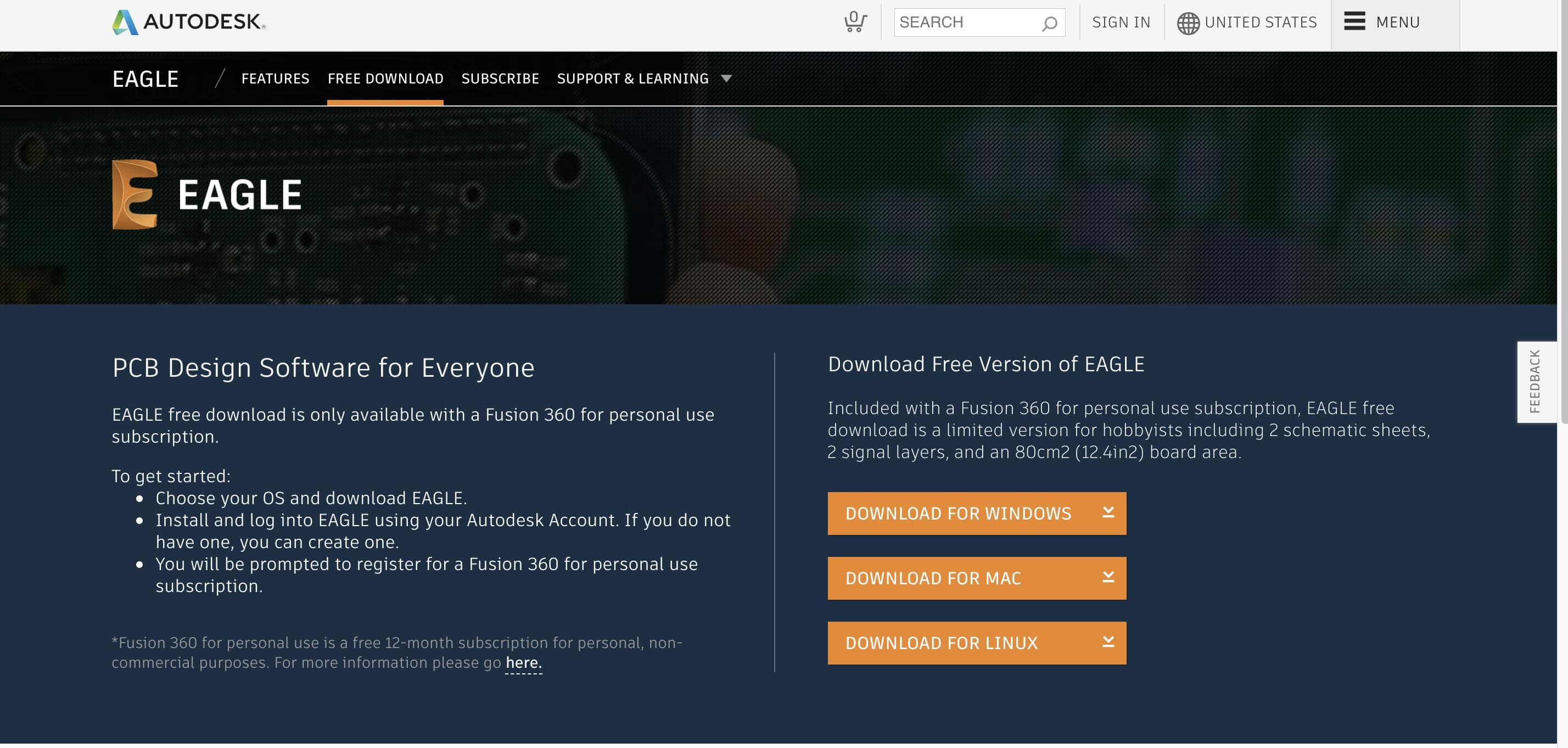
To start designing the PCB you need to download and Install the Eagle software which is electronic design software used for drawing printed circuit boards (PCB), connecting schematic diagrams, placing components, and tracing the routes.
DOWNLOAD EAGLE
I downloaded it twice on different laptops, because I use both Windows (HP) and Mac OS (MacBook Pro).Click Eagle to download it.
- Complete all the steps to install Eagle software.
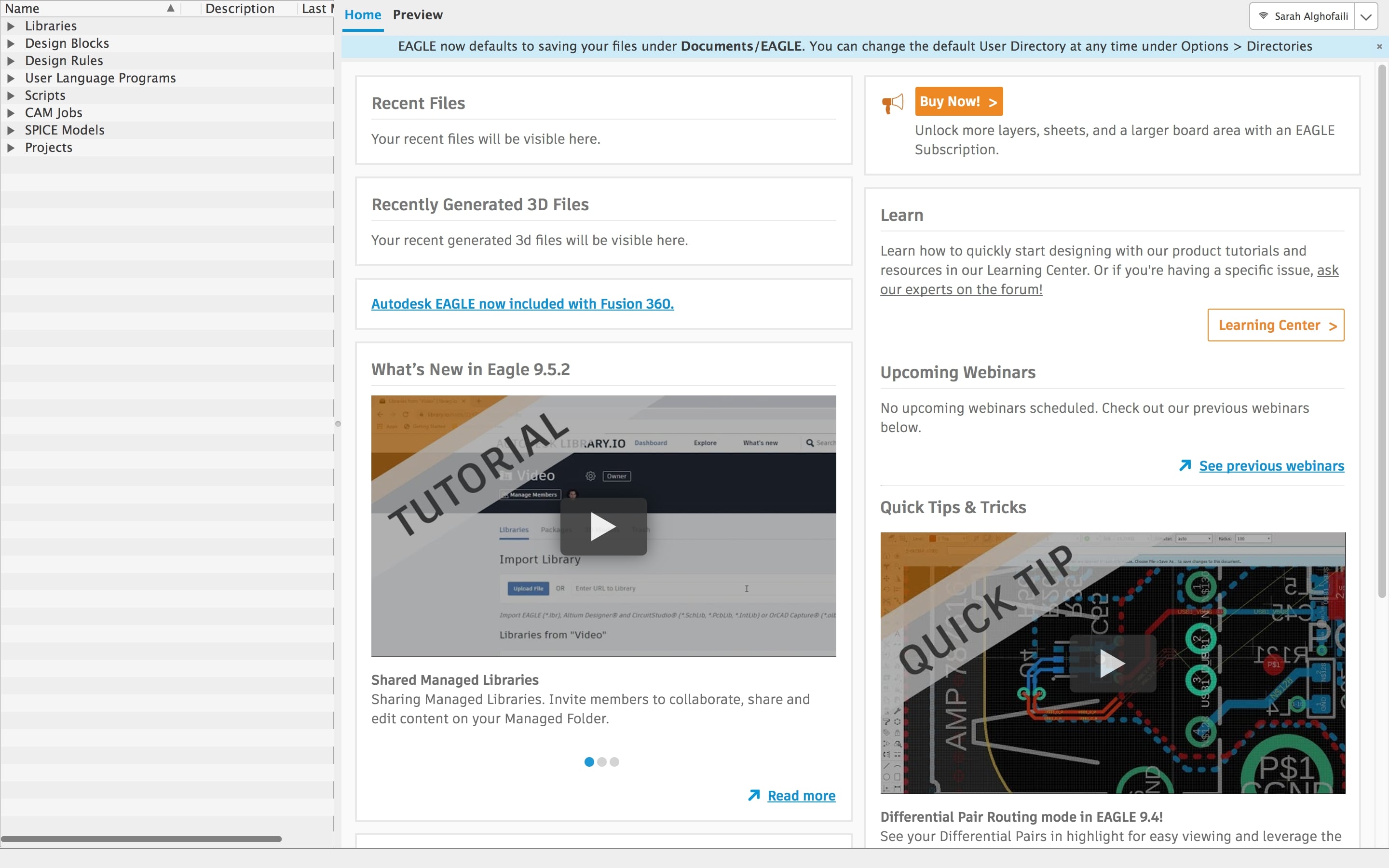
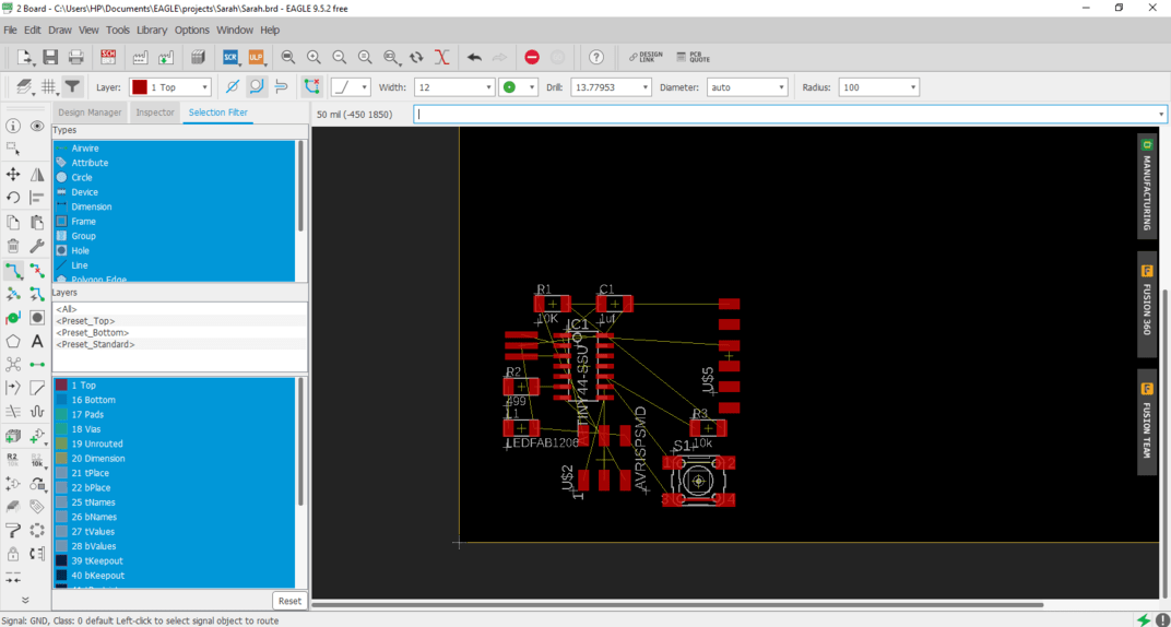
This the Eagle software interface:
THE COMPONENT LIBRARY
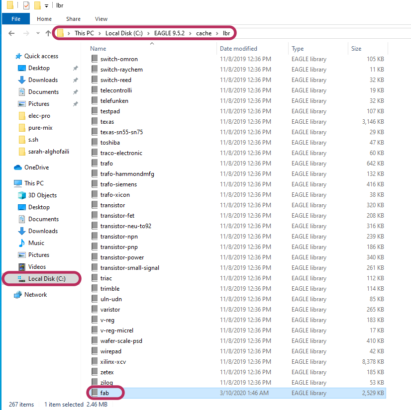
To design the Echo hello-world board you need to download the Fab library which contains all the components that are used in this PCB. You can find it here Fab.lbr.
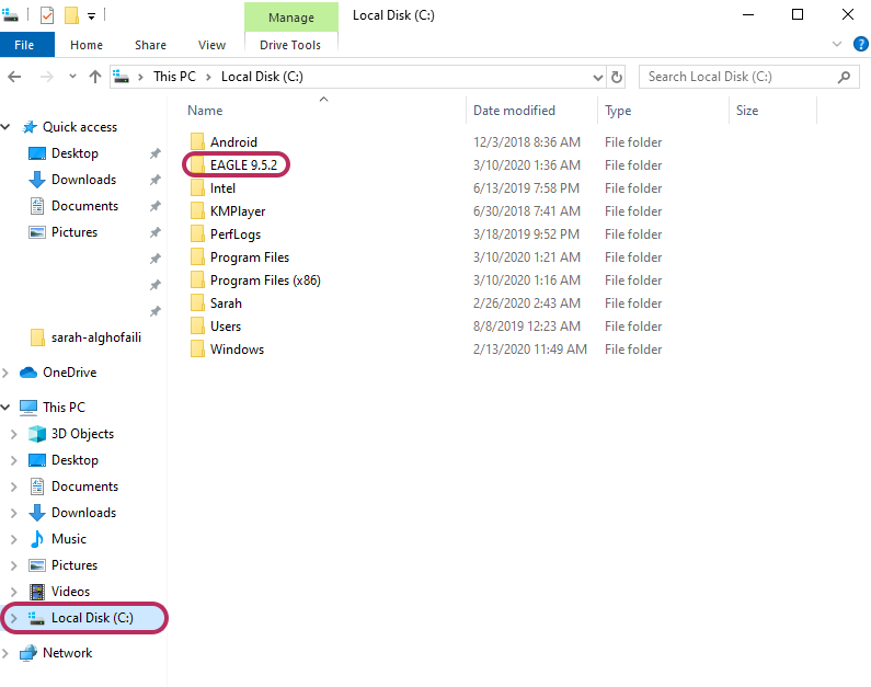
After the Fab library has been downloaded, I placed it in the “Lbr” folder by following this step: C: > Program Files > EAGLE 9.5.2 > Catch > lbr > drag the library file here.
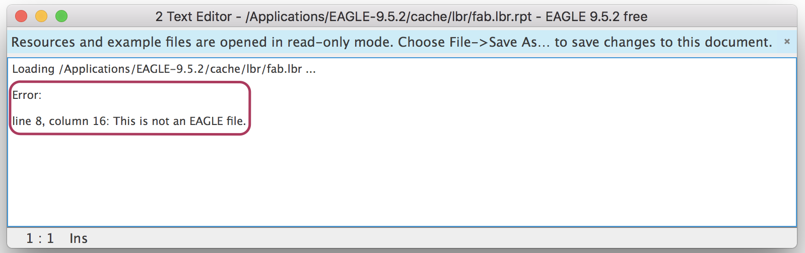
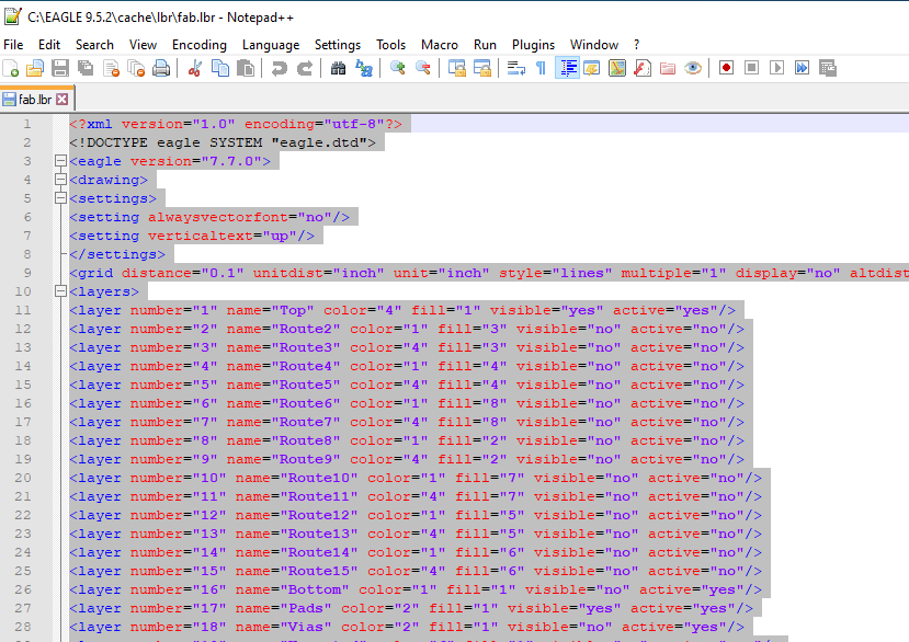
Then, I had an issue while adding the fab.lbr file to the Eagle library. Each time that I try to add it, I keep getting this error: “ line 8, column 16: This is not an EAGLE file.”
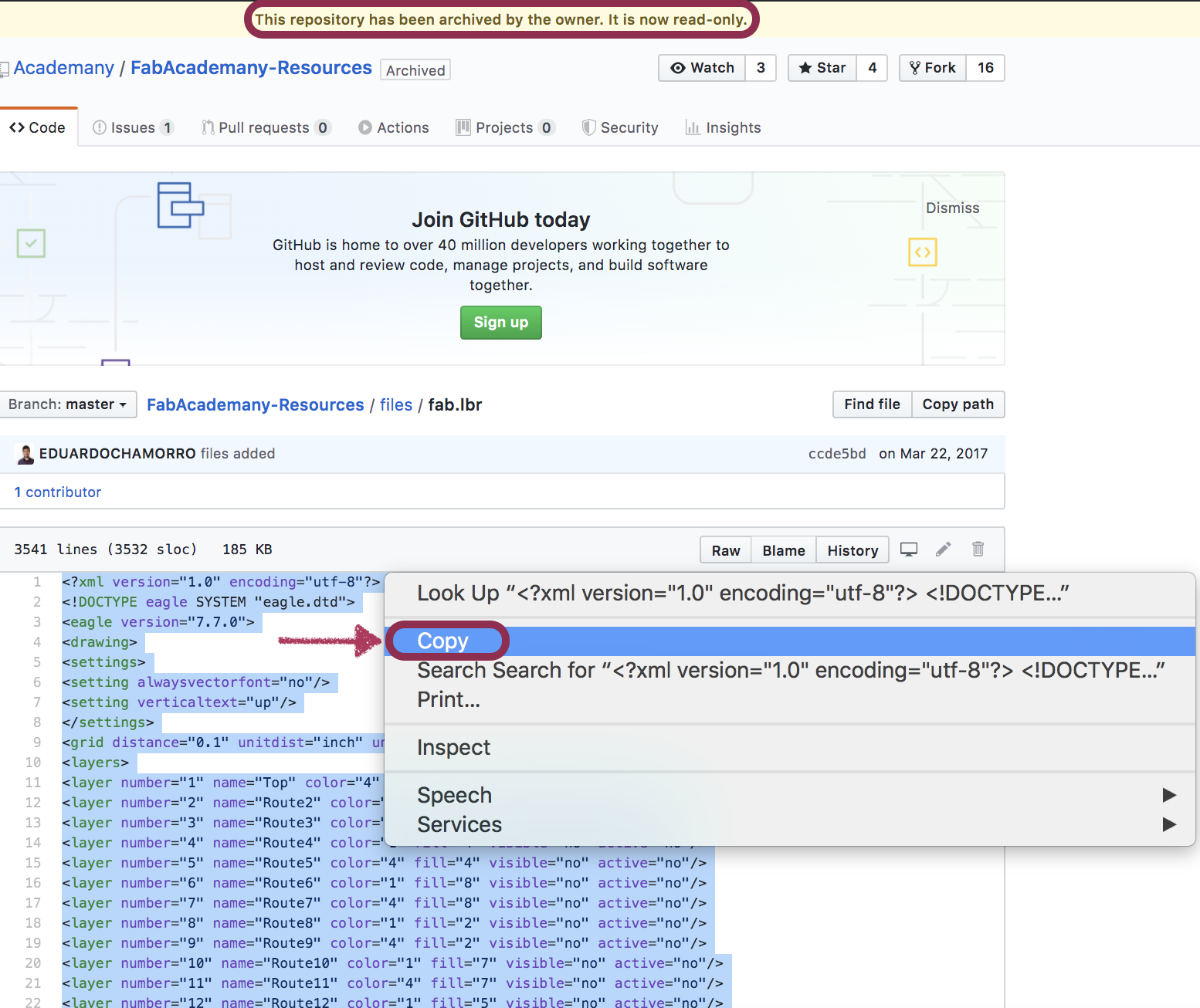
To solve this problem , our Instructor Mr.Yousef Alsinwar advised me to:
- open the Github link and copy the text.
- Replace the text in the fab.lbr file via Notepad++ :
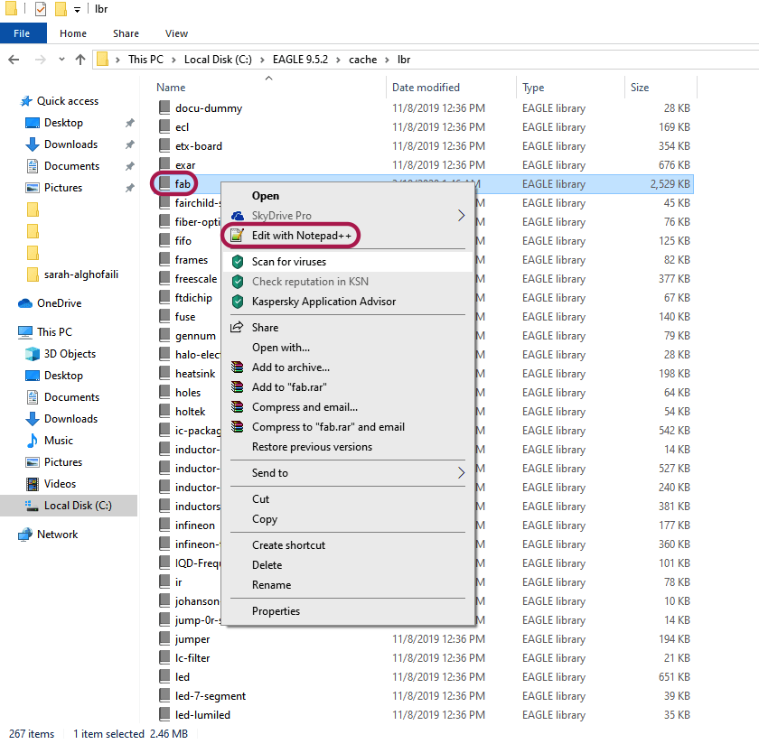
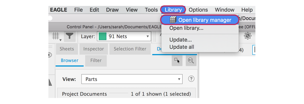
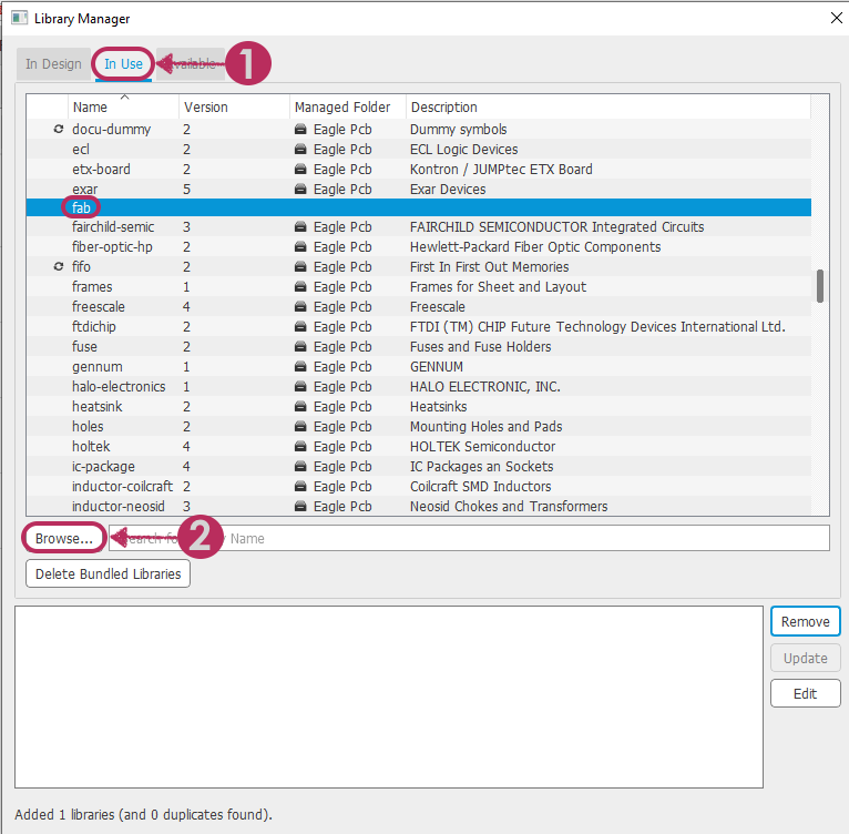
Now, to add fab.lbr file to the Eagle library, from the Eagle software menu bar : Library > Open library manager > In Use > Browse > C: > Program Files > EAGLE 9.5.2 > Catch > lbr > fab.lbr
Problem solved !
DESIGNING THE PCB
To design the PCB using Eagle software, I have to make a schematic diagram and Board Layout.
The schematic diagram allows you to define the PCB components and their pins connection electrically. In contrast, The board Layout allows you to place that PCB components physically on the board.
SCHEMATIC DESIGN
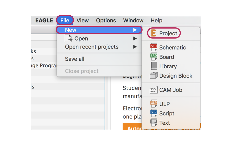
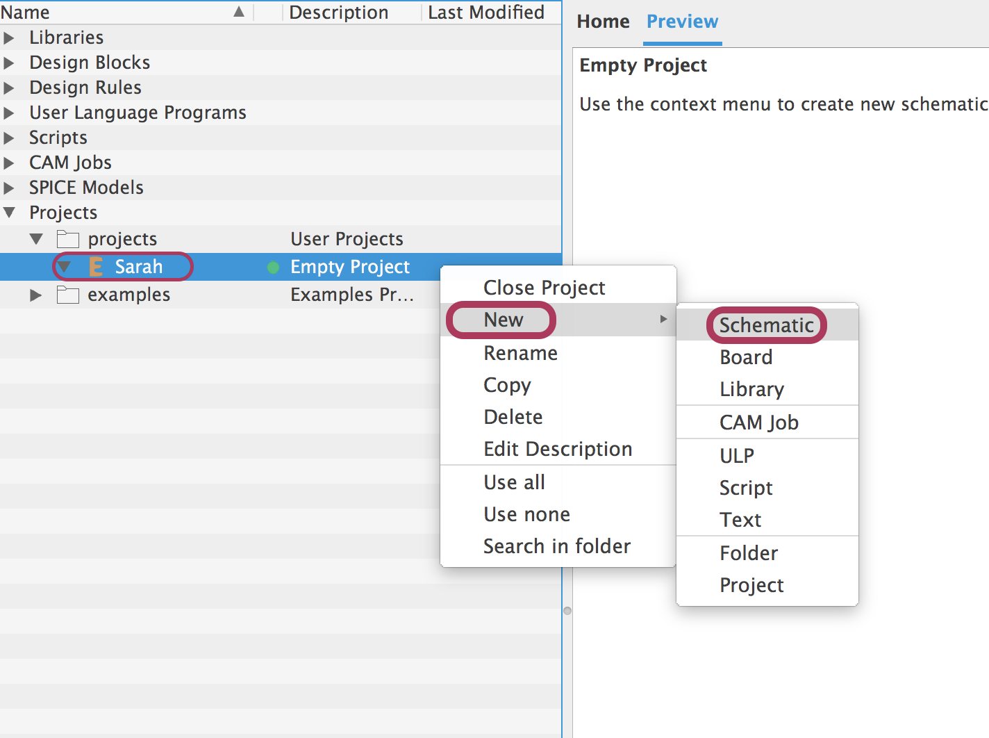
To create a Schematic, I created a new project first by clicking on File > New > Project. Then I gave it a name.
Then, I created the Schematic by selecting the project > Right click > New > Schematic
This is the schematic interface. It includes many useful tools, I will explain some of them.
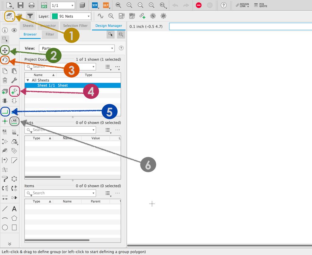
(1) Manage the visible layers by specifying which layer is hiding or showing.
(2) Moving tool used to move objects.
(3) Rotation tool that used to rotate the objects.
(4) Add Part tool to add a new component.
(5) Net tool that used to create connections between the components.
(6) Label tool that used to add text to the wires and make a connection without drawing wires.
(7) Adding value to value some part for example: resistors and capacitors
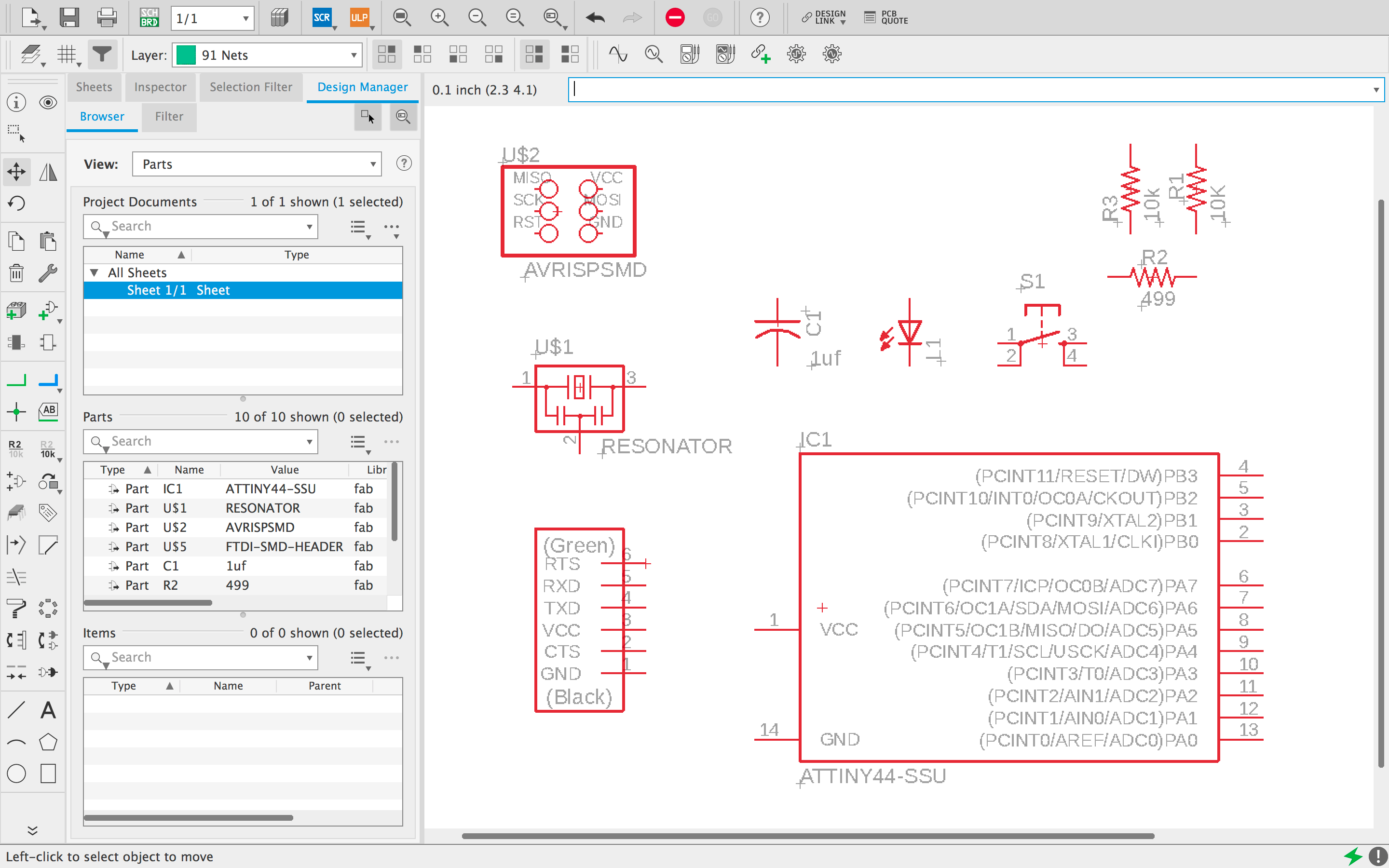
PLACING COMPONENTS
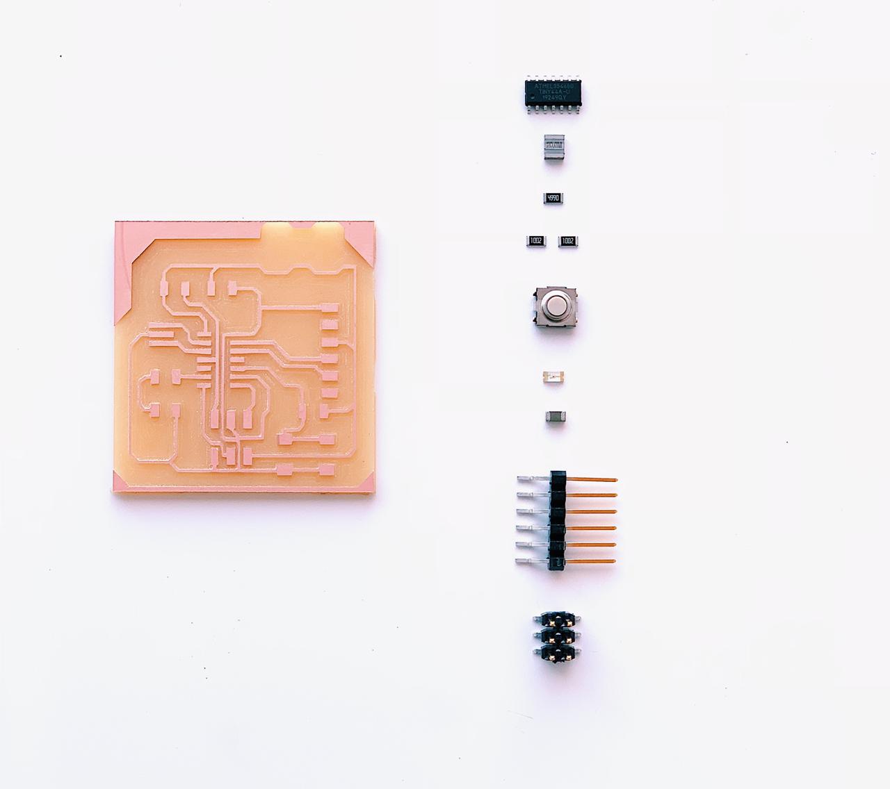
I Identified all the components to make it easy to find in the library.
The components list:
attiny44 microcontroller
6-pin programming header
FTDI header
20MHz resonator
2X 10k Resistor
Button
Ground
VCC
LED
499 ohms Resistor
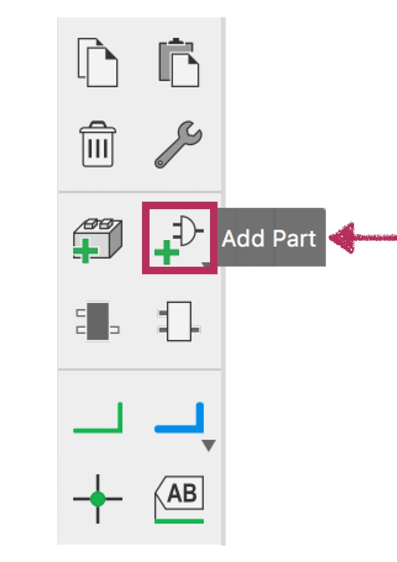
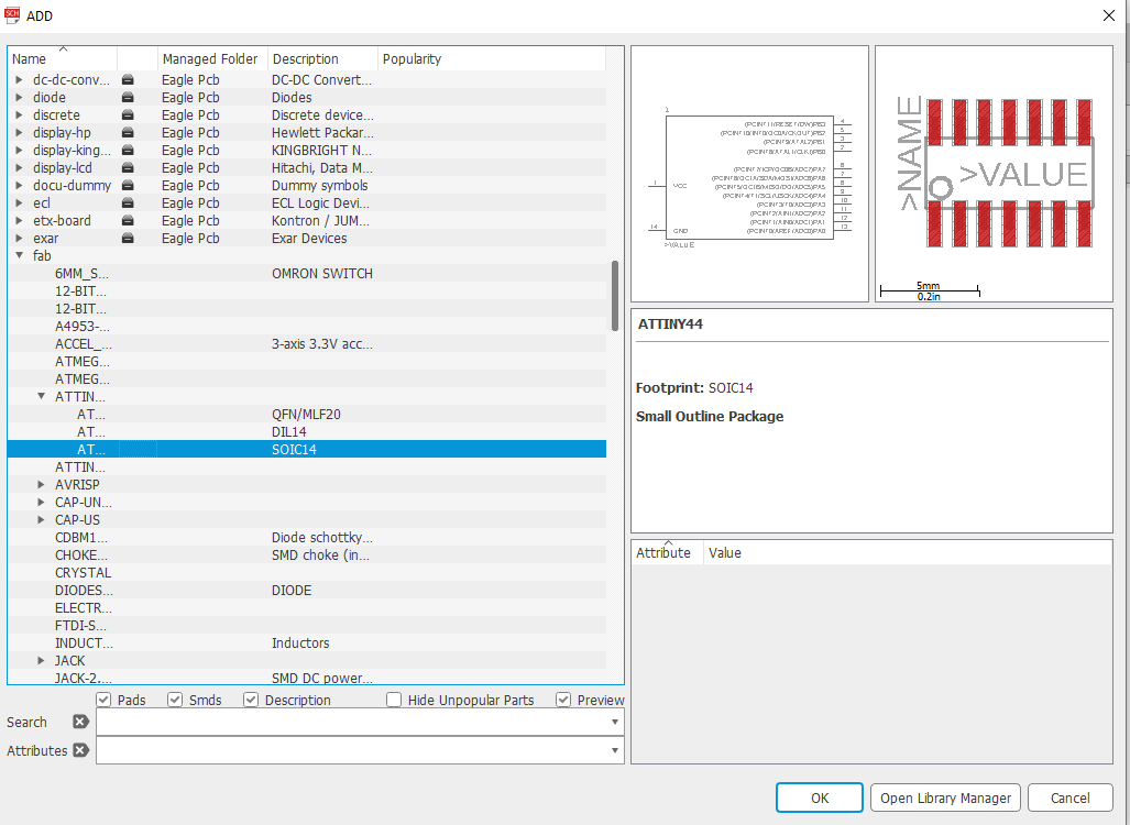
I used the “Add part” tool to search on each component from the library and add it to the schematic.
After placing all the components from the Fab library, I arranged the parts to prepare them for the connection.
CONNECTIONS
The next step in creating a schematic diagram is route wires between the parts. From the left side menu I selected the Net tool icon then start the net connection by clicking on the end of the symbol and dragging the mouse to the other part.
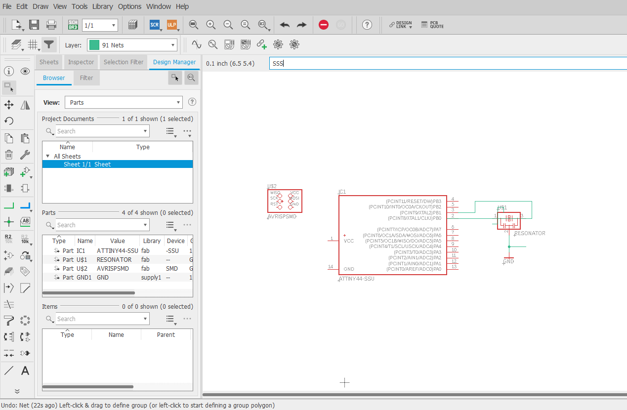
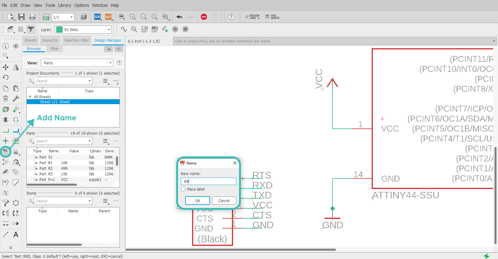
The step after that is assigning names to the components. “Name” is a unique identifier for each part. If we connect each part with Nets, the schematic will look ugly and hard to read. For that, I used the “Name” tool to make it easy to read the diagram.
If two nets have the same name they will be automatically connected. For example, I noticed these two nets have different names “RX” and “RXD”. For that I changed the net name RX to RXD using the “Name” tool to avoid the mismatch that may occur between the schematic and board.
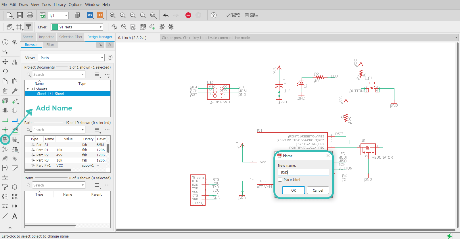
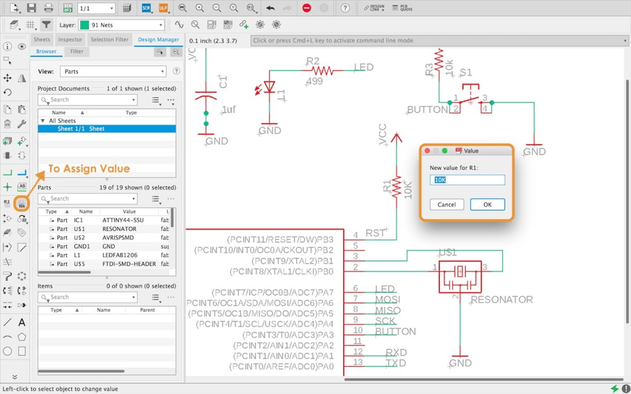
In addition, I used the “Value” tool that gives a specific value for each part to help in recognising the components place especially in the soldering process.
To assign actual value for simple parts like resistors and capacitors, I clicked on the “Value” button from the left toolbar.
THE BOARD LAYOUT
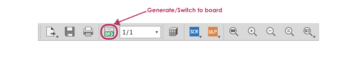
After drawing the schematic diagram, I generated the board by clicking on the Generate/switch button.
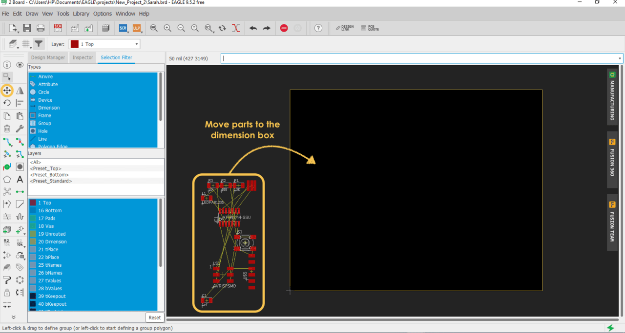
On the board, It looks messy ! but I arranged the components and created the routes between them by following this board layout in the Fab Academy tutorial.
Using the "MOVE" tool, I dragged all the components to the dimension box which is the physical dimensions of the board layout.
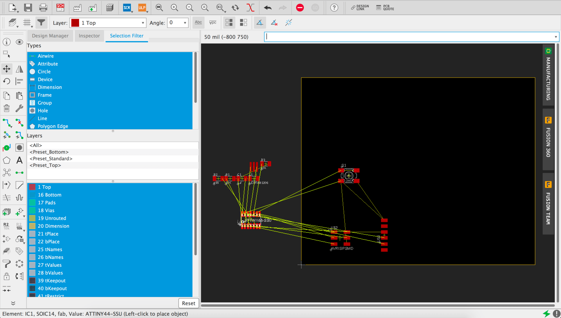
After moving all the components to the board area, I arranged them by focusing on minimizing the length of the yellow airwire connections.
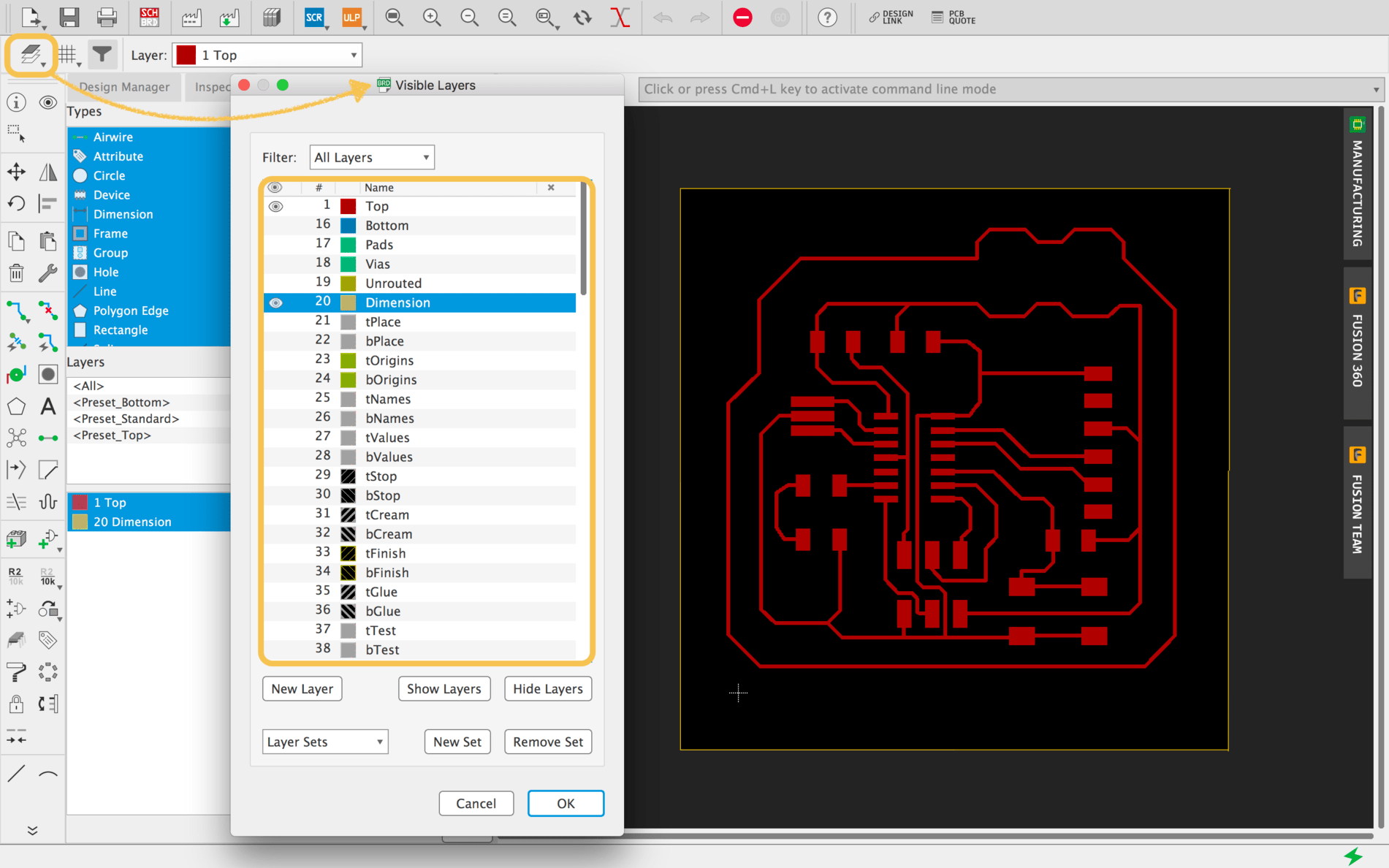
Before exporting the board, I need to hide the layer and show the top layer. I clicked on the visible layers tool from the top toolbar.
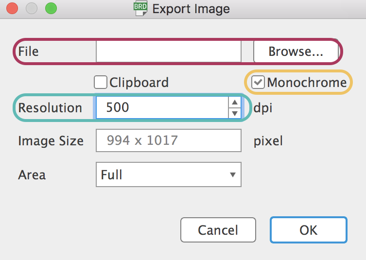
Now, to export it click on File > Export > Image
FABRICATING THE BOARD
PCB MILLING
As we have learned from the previous assignment “ Electronics Production “, the second step of the process of the PCB fabrication after designing is the milling process.
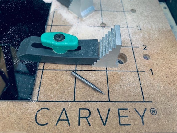
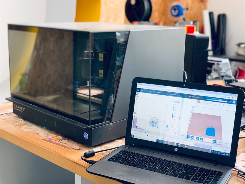
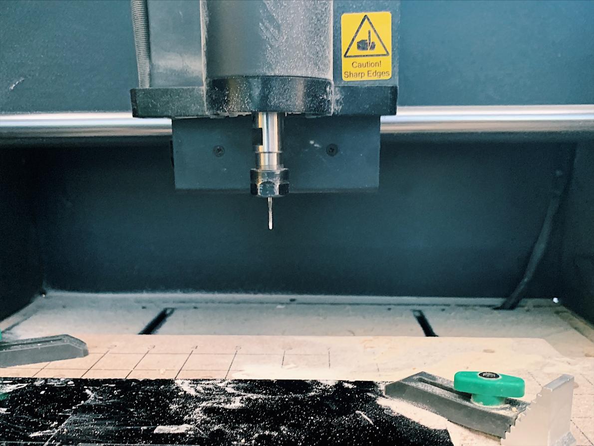
I prepared the carvey machine by placing the copper board on the workspace and putting a proper bit.
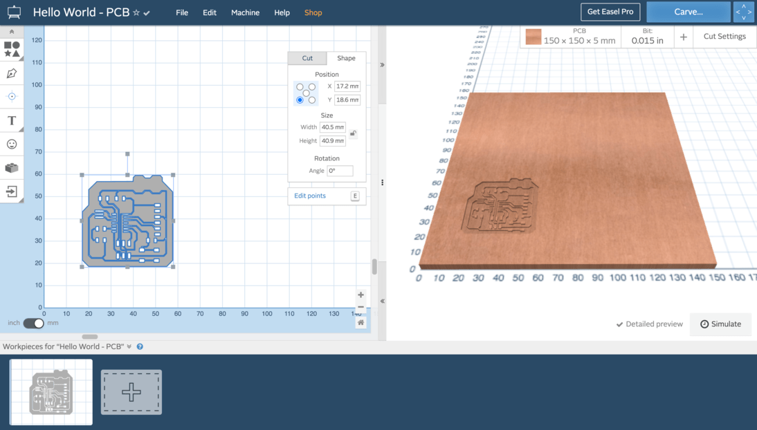
First, I opened the Easel software to import the echo hello-world board and assign these settings :
- Material : PCB
Traces :
- Bit size = 1/64 inch
- Depth : 0.1
- Feed rate = 180 mm/min
- Plunge rate = 90 mm/min
Outline :
- Bit size = 1/32 inch
- Depth : 5mm
Then, I prepared the carvey machine by placing the copper board on the workspace and putting a proper bit.
To start the milling process, I clicked on the “Carve” button to begin. Can’t wait to see the result !
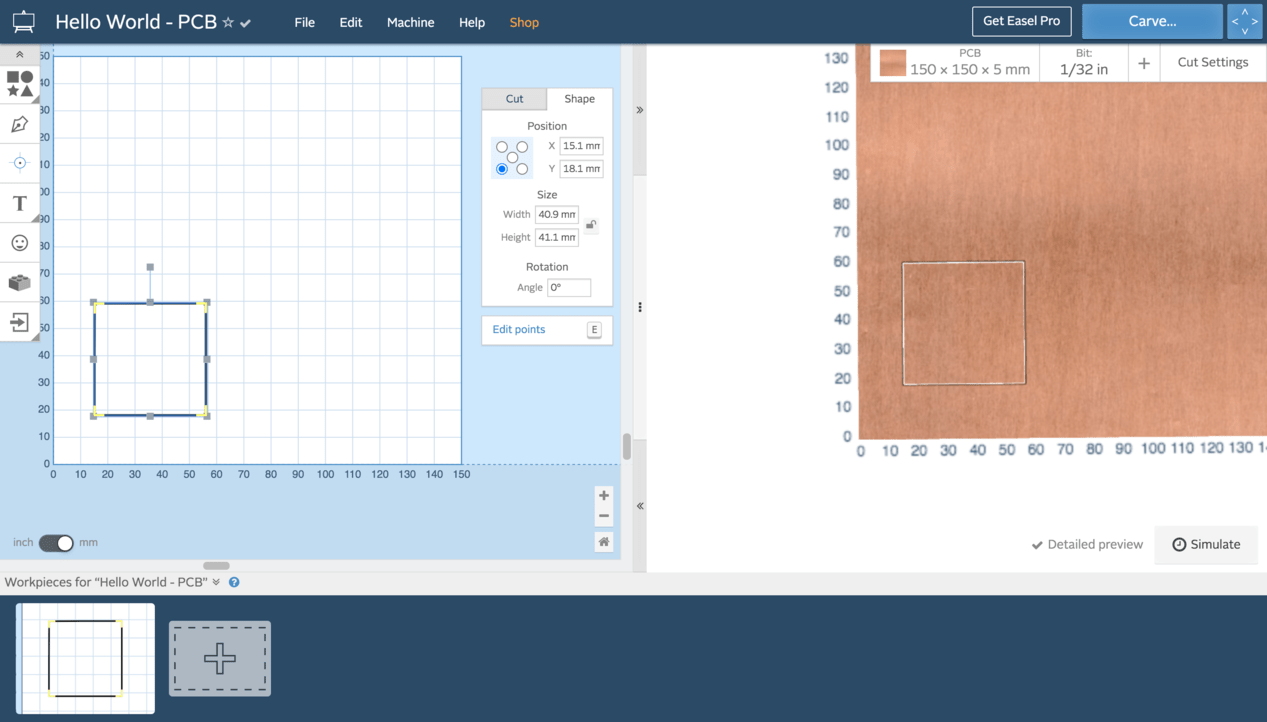
Next, I changed the bit to 1/32 bit to cut the outline.
Oops !
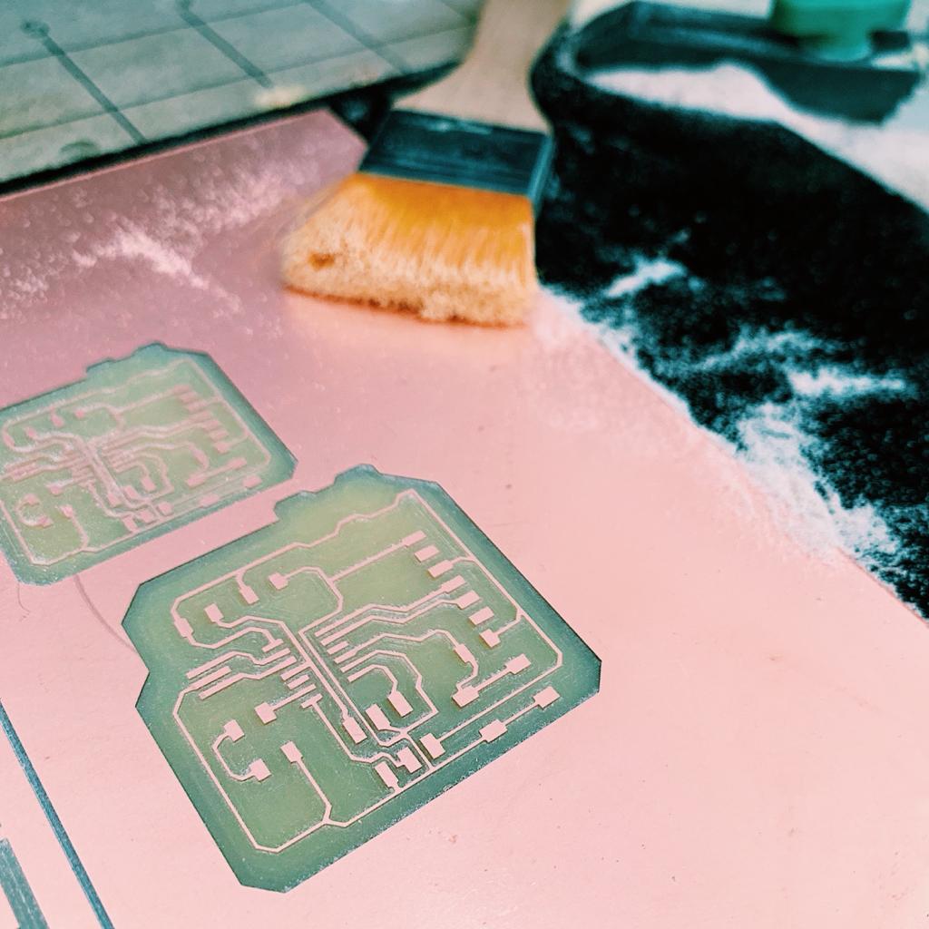
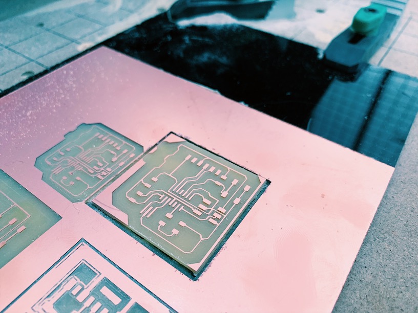
I noticed a small mistake in my PCB routes, there is a junction point between two paths but I removed it by using a cutter tool.
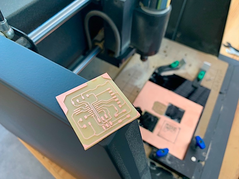
It looks perfect !
PCB SOLDERING
This part is my favorite !
After the "ELECTRONICS PRODUCTION" Assignment, I found that soldering the circuit boards was a satisfying experience for me.
To start the soldering process, I prepared all the components needed. Then, I used the iron after the warmed up. Next, I placed the microcontroller first and the rest of the components onto the board.
It is important to be careful to the iron temperature while soldering because an overheated iron can damage components.
PCB Testing and PROGRAMMING
Before starting programming the PCB I Installed Arduino IDE 1.8.5 that includes attiny 44 board.
To program the PCB, I followed some steps.
I started by I opening the Arduino IDE
preparing the UNO board for programming
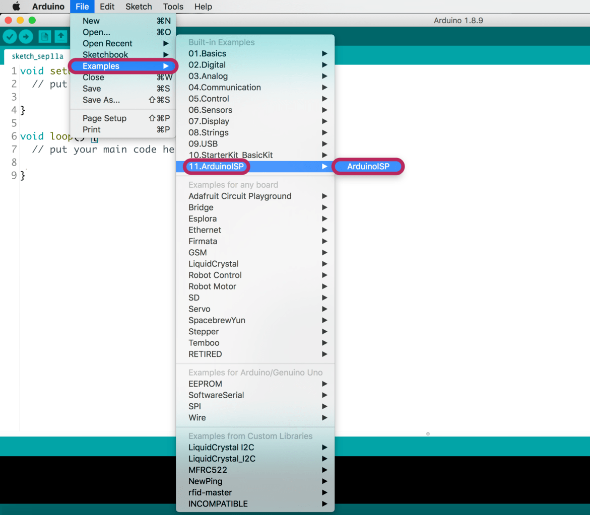
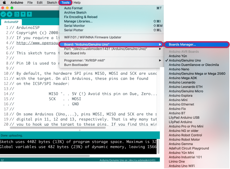
File > Examples > ArdionoISP > ArduinoISP
After that I connected my Arduino and uploaded the Arduino ISP program to transform it into a programmer for the Attiny.
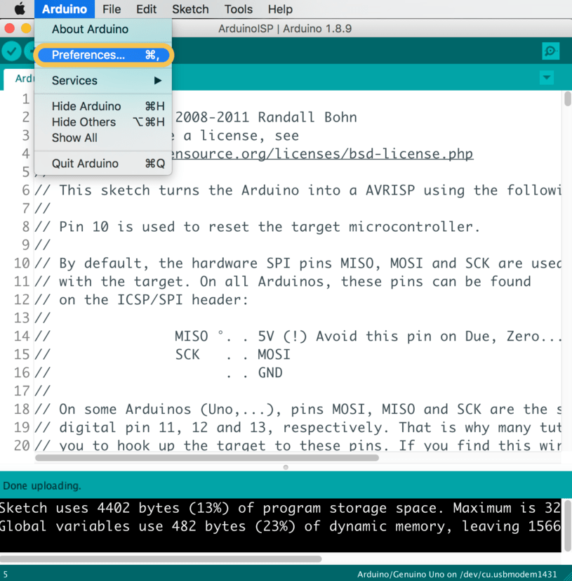
Setting Up the Arduino IDE
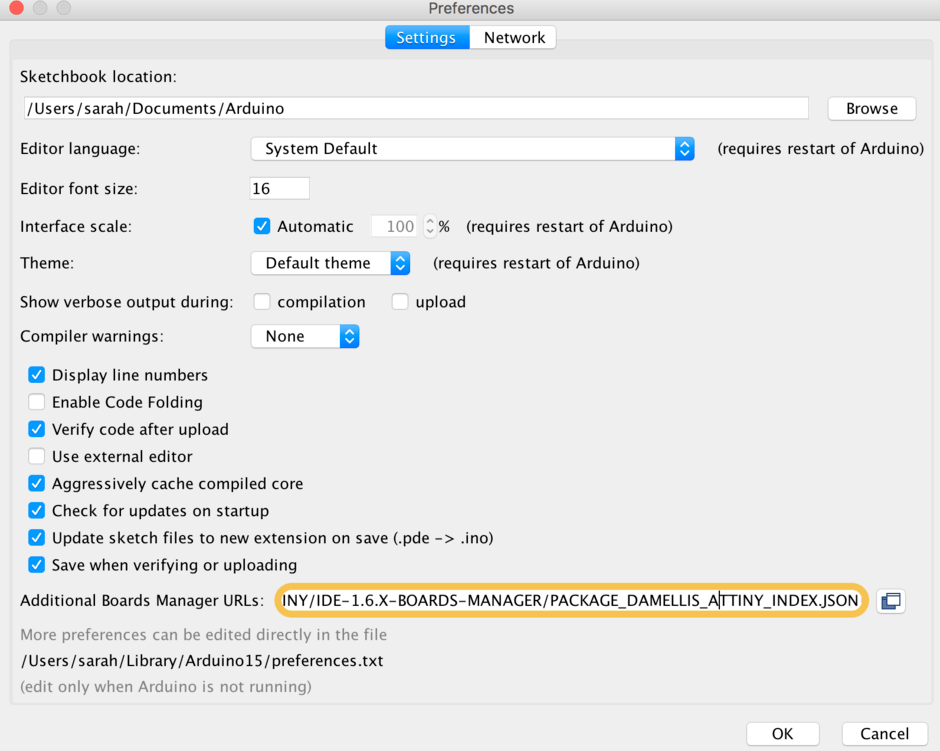
Go to File > Preferences
In the "Additional Boards Manager URLs:" I pasted this link:
https://raw.githubusercontent.com/damellis/attiny/ide-1.6.x-boards-manager/package_damellis_attiny_index.json
Next go to Tools > Boards > Boards Manager
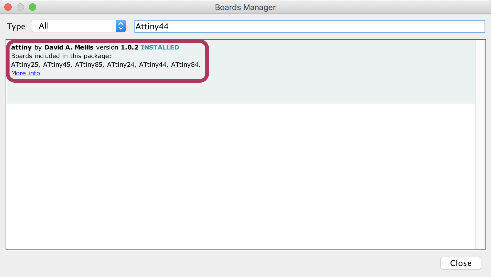
After that search for the attiny type attiny” attiny44” then Install it.
Programming the Attiny
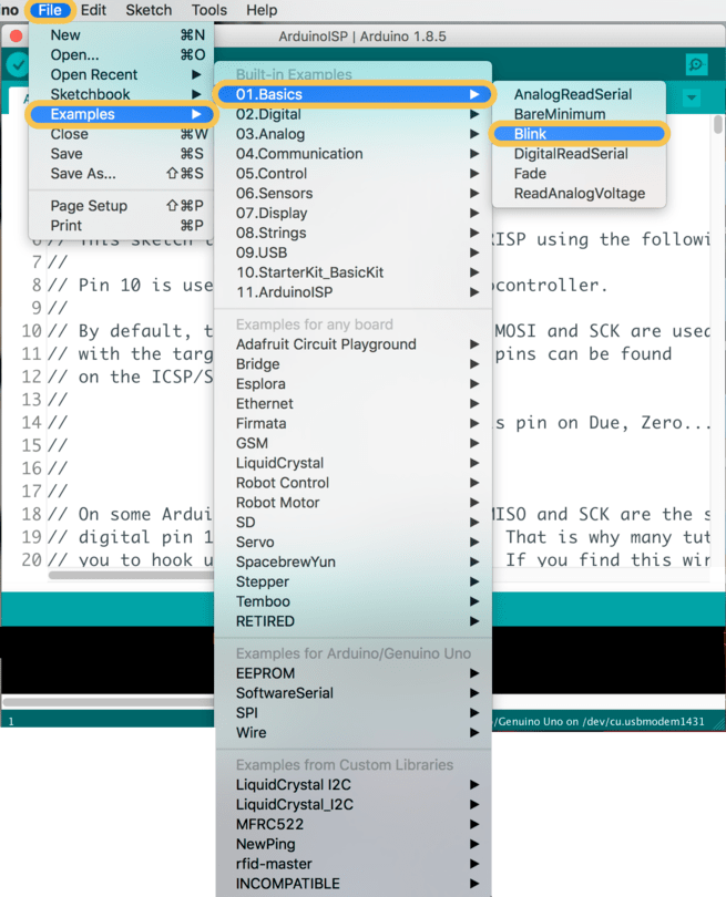
Then I added the Blink code
File > Examples > Basics > Blink
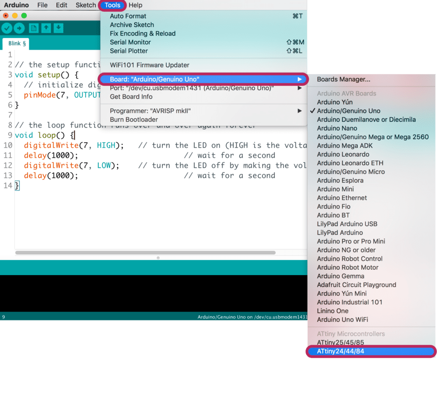
After that to select the board I clicked on
Tools > Boards > Attiny24/44/84
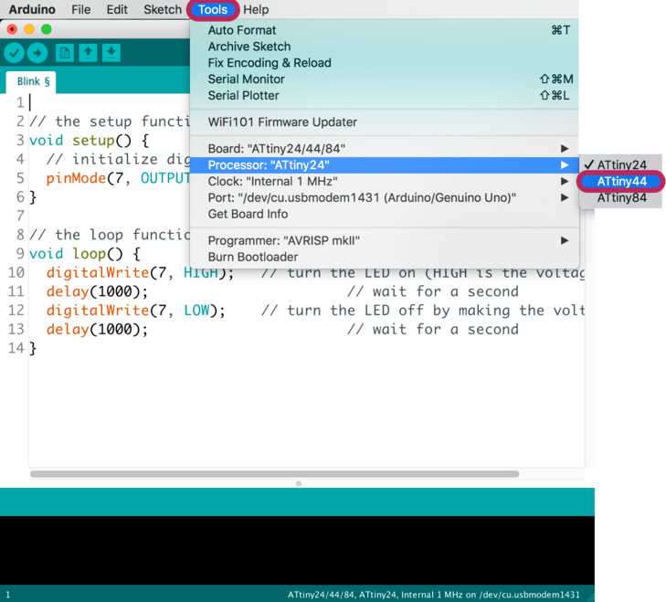
For the “Processor:" I selected the Attiny that I chose to use.
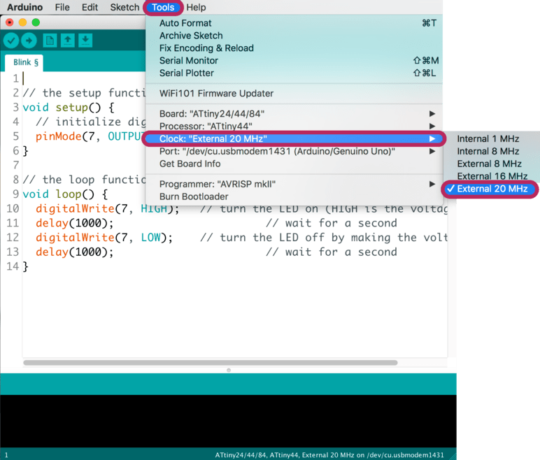
Next, I changed the clock speed of the Attiny
Tools > Internal 20 MHz
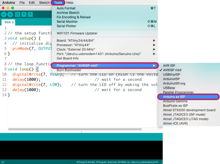
For the “Programmer:" I selected Arduino as ISP.
Finally, I uploaded the blink code to the Attiny by clicking on
Sketch >Upload using programmer
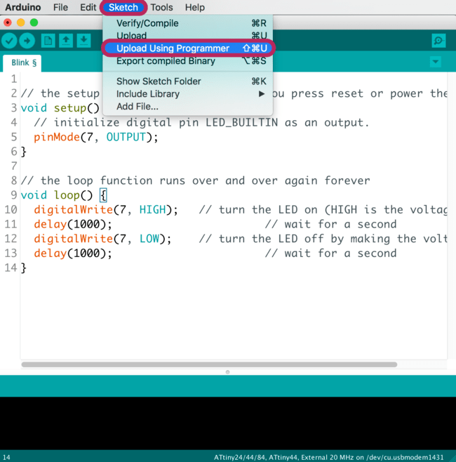
THE CODE " Blink "
The blink code will turn an LED on for one second, then off for one second, repeatedly.
The code includes two functions:
1. Void setup
2. Void loop
In the Setup section :
"pinMode()" function is used to initialize pin 7 as digital output.
Set the pin to HIGH (5V) to turn the LED on.
call delay() which delays the number of milliseconds that means the LED will Wait for 1000 milliseconds, or one second.
Set the pin to LOW(0V) to turn the LED off.
Wait for another second, and then repeat everything again.
In the Loop section :