Exercise 6 - Electronic Design 4/3/2020 to 12/3/2020
There are 2 tasks for this week:
- Group Assignment: Use the test equipment in the FabLab to observe the operation of a microcontroller circuit board
- Individual Assignment:
- Use an EDA software to modify an echo hello-world board by adding at least a button and LED
- Check the design rules
- Make the board and test it (Scope is the same as Exercise 4)
Group Assignment:
Use the test equipment in the FabLab to observe the operation of a microcontroller circuit board
This group assignment is done with Noel Kristian and Yeo Gau Siong.
Our collective work is documented on the SP Fablab Website and hence only my learning and reflections are documented here
What I have learned:
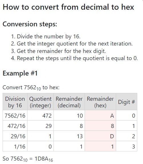
- About Hexadecimal and Hexadecimal Numbering System
- Hexadecimal Numbering System is commonly used in computer and digital systems to reduce large strings of binary numbers into a sets of four digits for easy understanding
- There are 16 distinct counting digits from 0 to F. In order to distinguish Hexadecimal numbers from Denary numbers, a prefix of either a “#”, (Hash) or a “$” (Dollar sign) is used before the actual Hexadecimal Number value, #D5CF or $D5CF.
- Example:
References
www.electronics-tutorials.wswww.rapidtables.com/convert/number/decimal-to-hex.html
- Basic Electronics
- It has been several decades since I last learnt about electronics components and component symbols. This week's assignment provided me the opportunity (or stress) to refresh my memories on this topic. As good comprehensive website on basic electronics are easy to find, I am glad to be able to recall most of the basic stuff I have learnt in my Uni days and become more confident in completing this week's individual assignment
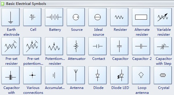
Image from : www.edrawsoft.com
Websites I referred to
www.instructables.com/id/Basic-Electronicswhttps://www.build-electronic-circuits.com/how-to-learn-electronics/
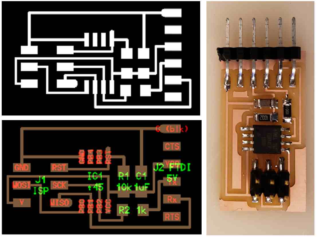
In Week 4, we have made an ISP programmer, the assignment this week is to make a target board that can be programmed using the ISP programmer that I have built. For Week 4's assignment, the board layout in PNG format can be downloaded. I simply have to load the file in MODS to generate the GCode files for the milling machine.
For this assignment, only image of the board layout and photo of the completed board are available, so in order to make modification, a new board must be created from the beginning, starting with schematic.
Information Available from FabAcademy.org
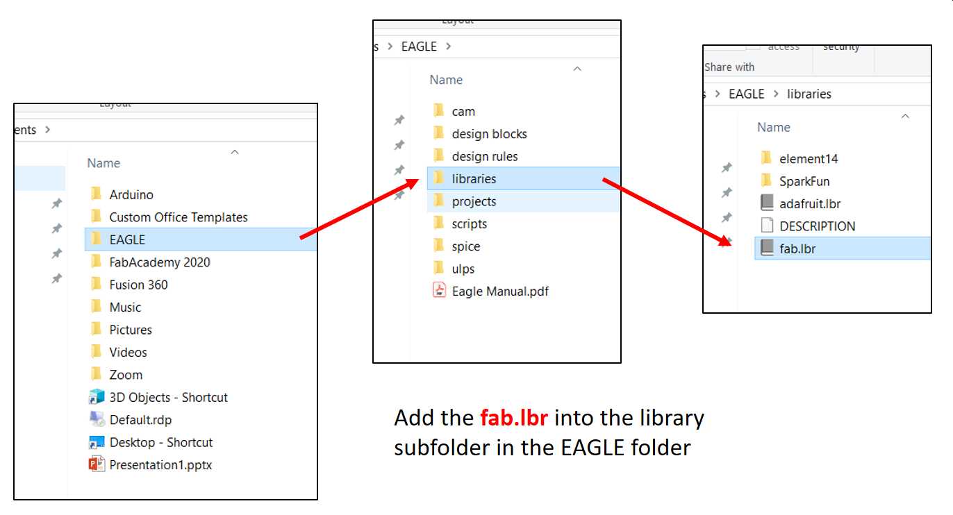
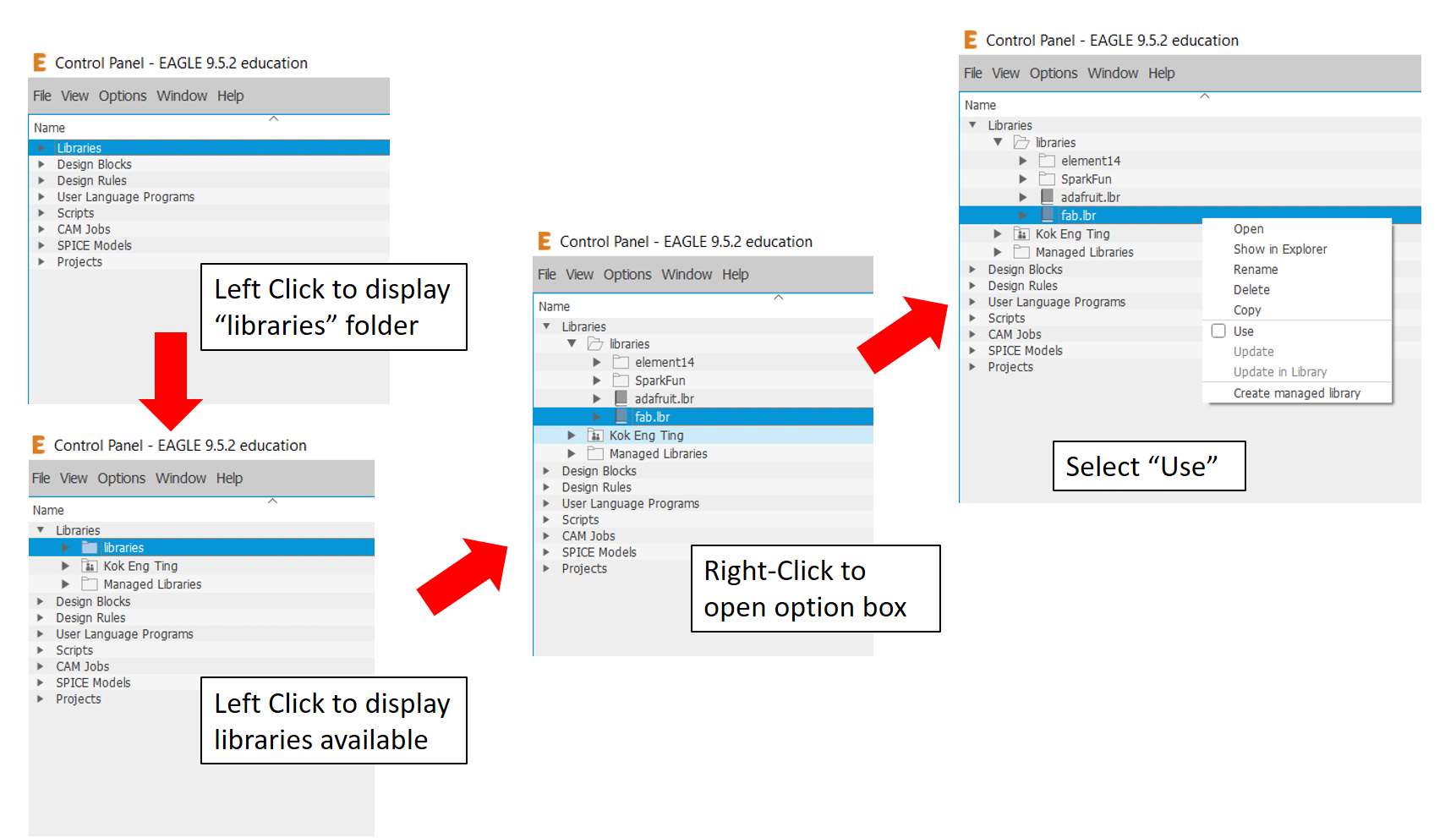
To add the library, there are several steps:
- Save the fab.lbr folder into the EAGLE library subfolder
- Open EAGLE and Select the libraries to use
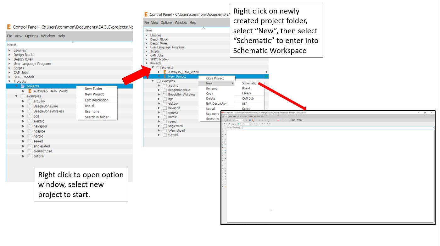
To start drawing the Hello_Board, a new project must first be created in EAGLE. The steps are captured in the image below:
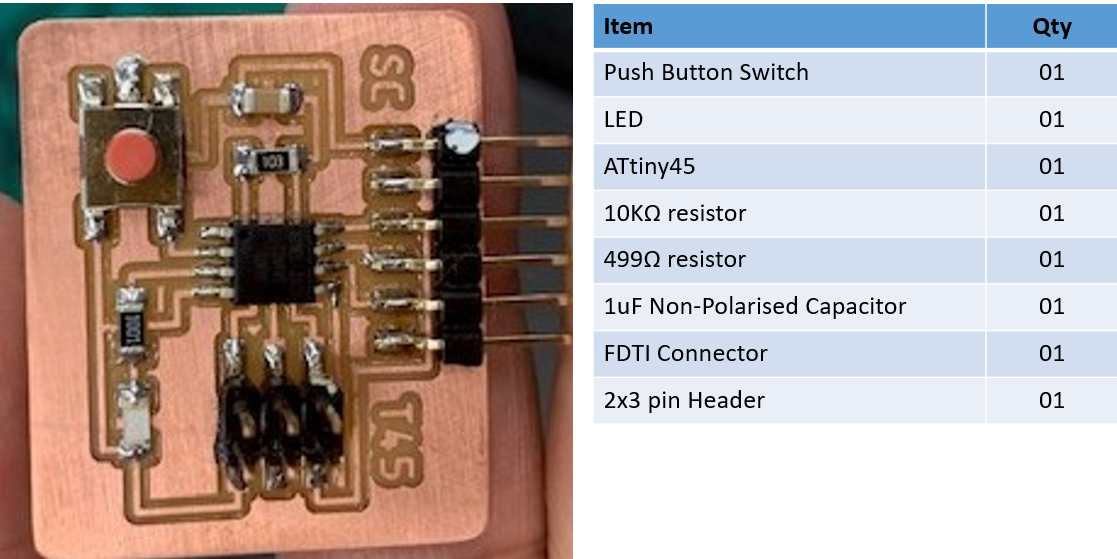
The next step is to populate the schematic workspace with all the required components for the Hello_board. At this juncture, I still have no concept on electronic design. Hence I decided to reverse engineered a Hello_board made by my coach, Mr Steven Chew. From the photo of his board, I obtained the following part list.
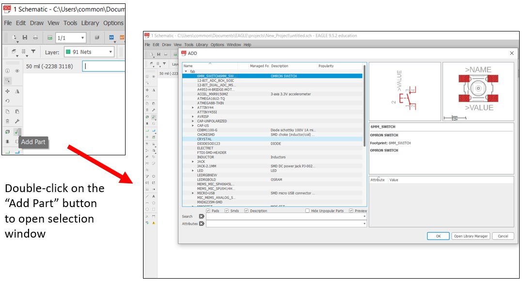
Adding the required components on the workspace
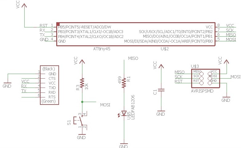
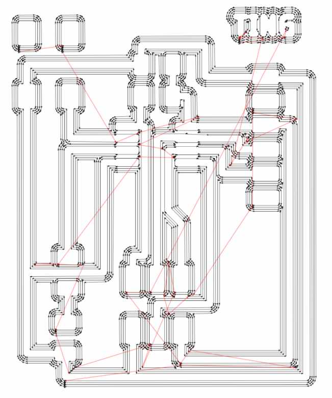
After populating the workspace, the next step is make all the necessary connections. The completed Schematic diagram is as follows:
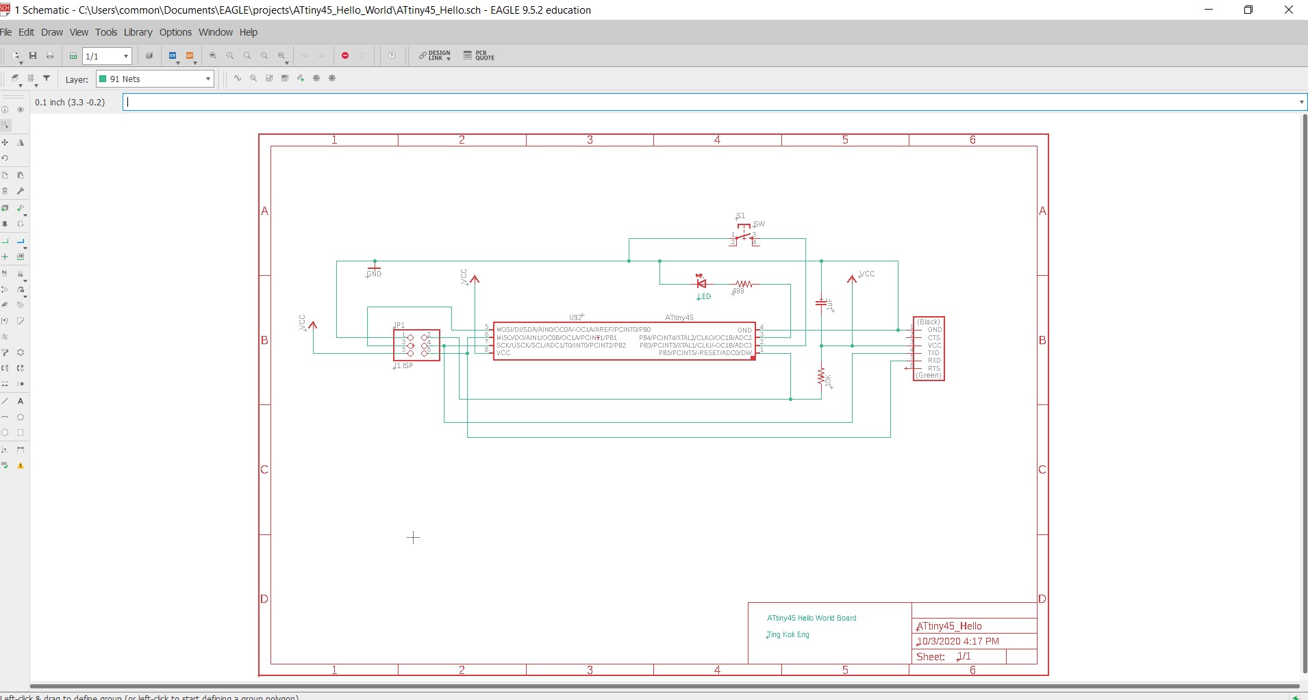
Completed Schematic; quite messy
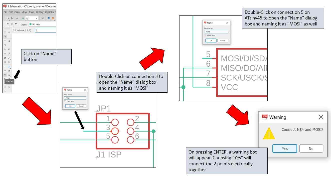
Instead of routing every component to every terminal, there is a better and neater way to do it. By using the Name command, two terminals are electrically connected when the same name is given.
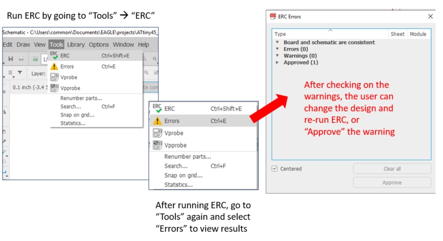
Upon completing the schematic, Electrical Rules Check (ERC) check must first be carried out to ensure that the connections are correct, and also to manually ignore unconnected points.
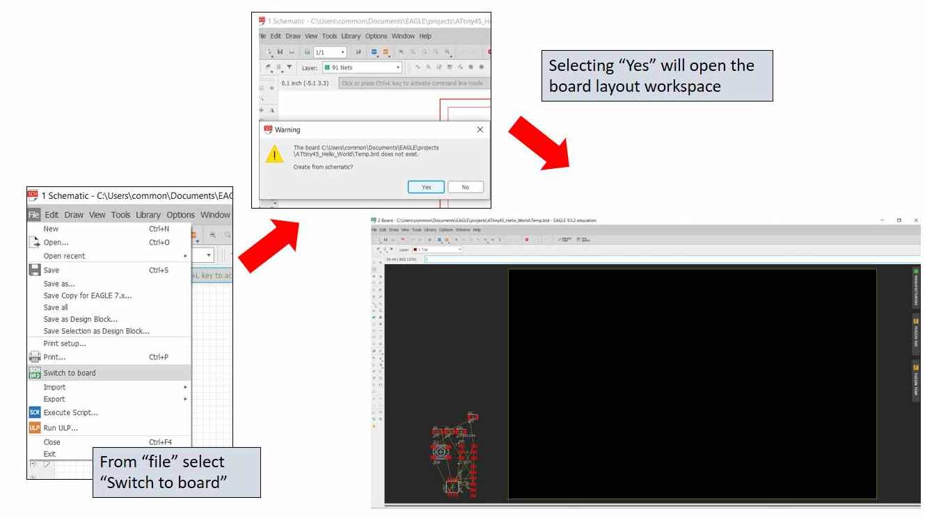
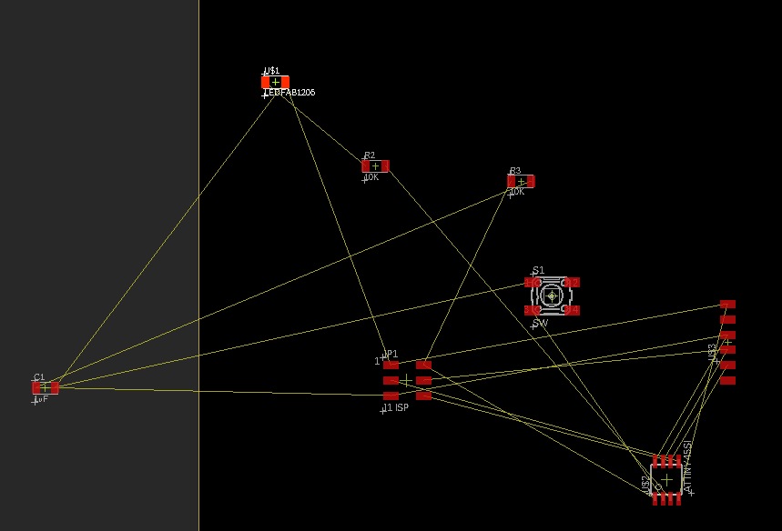
After clearing ERC, the next step is to design the board. From the file menu, clicking on "Switch to board" will open up a board layout workspace. The footprint of all the components as well as their electrical connections are all displayed in a "mess" at the bottom left corner.
To start the board layout, the components are first dragged to the workspace. While it is entirely based on the liking of the design, in laying out the board, it is good that best practices in placing components are referred to an followed. I used Altium.com as reference. Some of the points are listed below:
- connectors should be place to the side of the board
- orient similar components in the same direction, to make routing and soldering easier.
- placement of power points
- trace widths; 0.010” width for low current analog and digital signals, wider for more than 0.3 A should be wider.
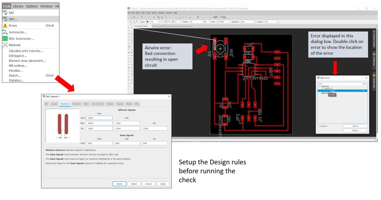
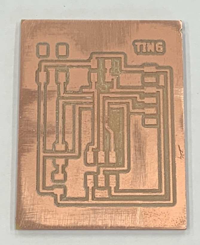
After arranging the components on board, the next step is to route all the airwires.
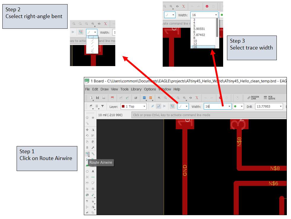
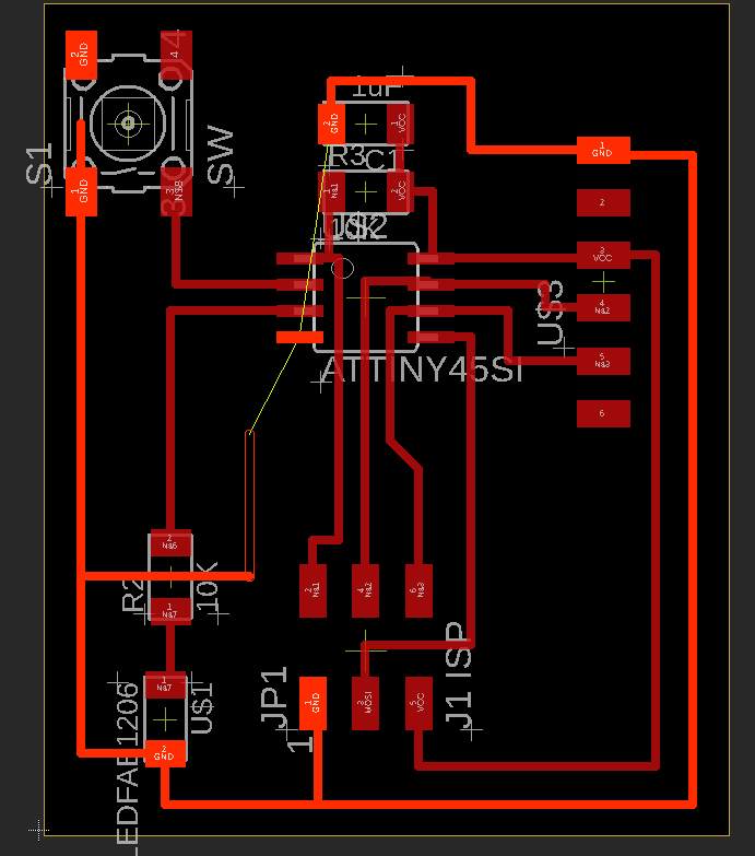
Upon completing the airwire routing, DRC (Design Rule Check) must be run to ensure that the board can be fabricated. The DRC can be found under the "Tools" menu. Before running the DRC, the parameters must first be setup. From the characterisation test, the minimum spacing that can be milled using the 0.4mm flat-end mill is 16 mils, hence for the DRC check, I used 16 mils.
Click Here to download Eagle Board Layout file.
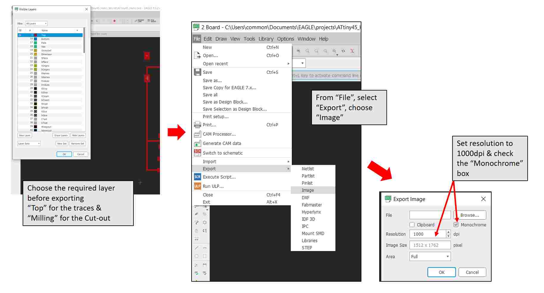
After clearing all the routing errors, the generation of the Gcode file for board milling can commence. To do this, I followed the tutorial on FabAcademy Tutorial
The steps are summarised in the image below:
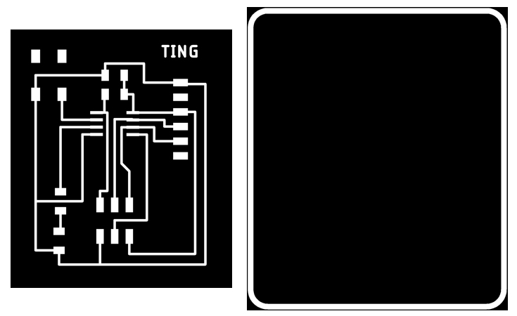
Click Here to download board outline file in PNG format.
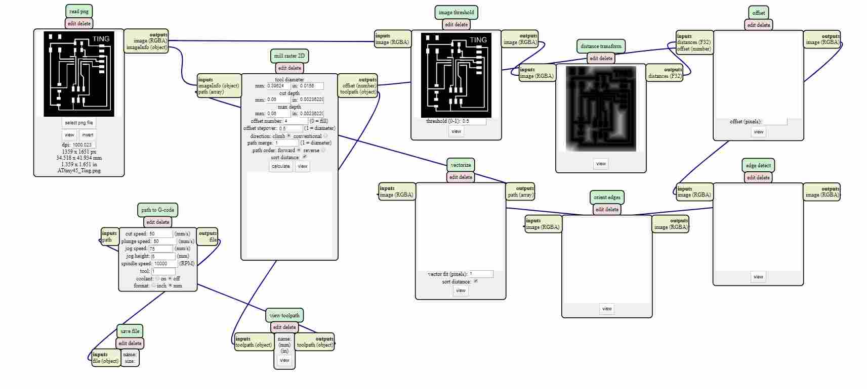
The preview of the gcode file
Click Here to download outline gcode file.
Milling and Cutting is done using the StepCraft 420 Milling machine. For the traces, 4 passes each with an offset of 0.5 times the tool diameter is used to remove as much dead copper as possible as I was going for isolation-milling. A 0.1mm 10 degree V-shaped drill bit was used instead of the 0.4mm flat-end mill that was used for characteristion due to non-availability of the latter in SP Fablab at the moment.
(the outline is not cut as the milling process was interrupted by unforeseen circumstances and the alignments were all off. Machine schedule does not allow re-calbration and testing)>
With the practice from Assignment 4, soldering this time is much more smoother, although the quality still requires much improvment.
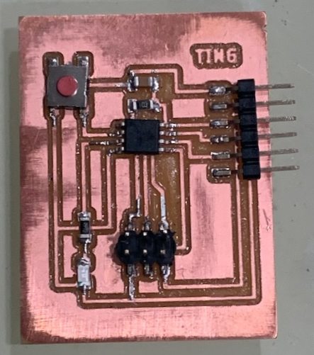
Testing the Board
To test if the board is successfully built, programing must first be done. The ISPtiny programmer that I made in Week 4 is used to program this board. For the software, our coach suggested Ardunio IDE as the learning curve is not as steep. For ATtiny45 to work with Ardunio IDE, additional board manager must be added.
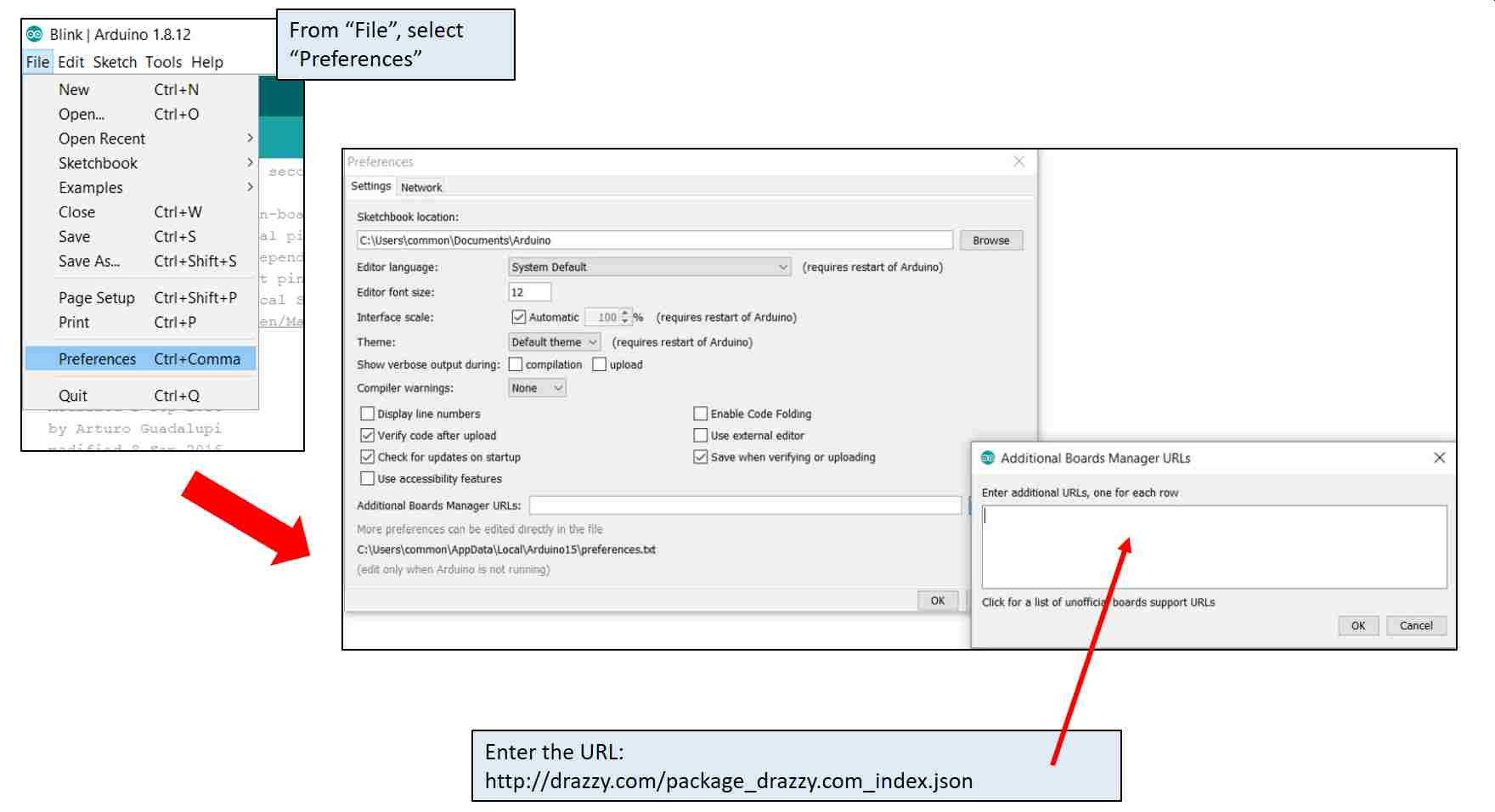
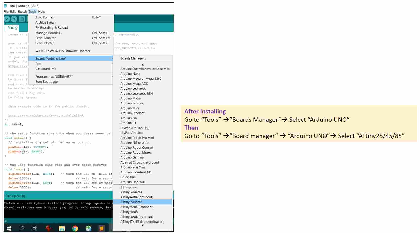
The URL (http://drazzy.com/package_drazzy.com_index.json) points to the cores that Spence Konde wrote to enable Ardunio IDE to work with ATtiny chips. Select the required Core and click install
After installation, the correct board manager needs to be specified.
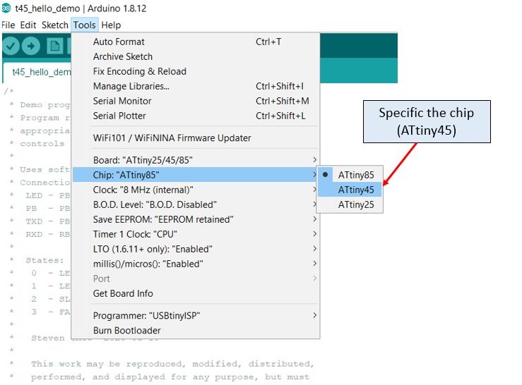
Next is to select the correct chip (ATtiny45)
Following that, the next step is to program the chip. The test program written by our coach, Mr Steven Chew, is used. The program file is first loaded in Arduino.
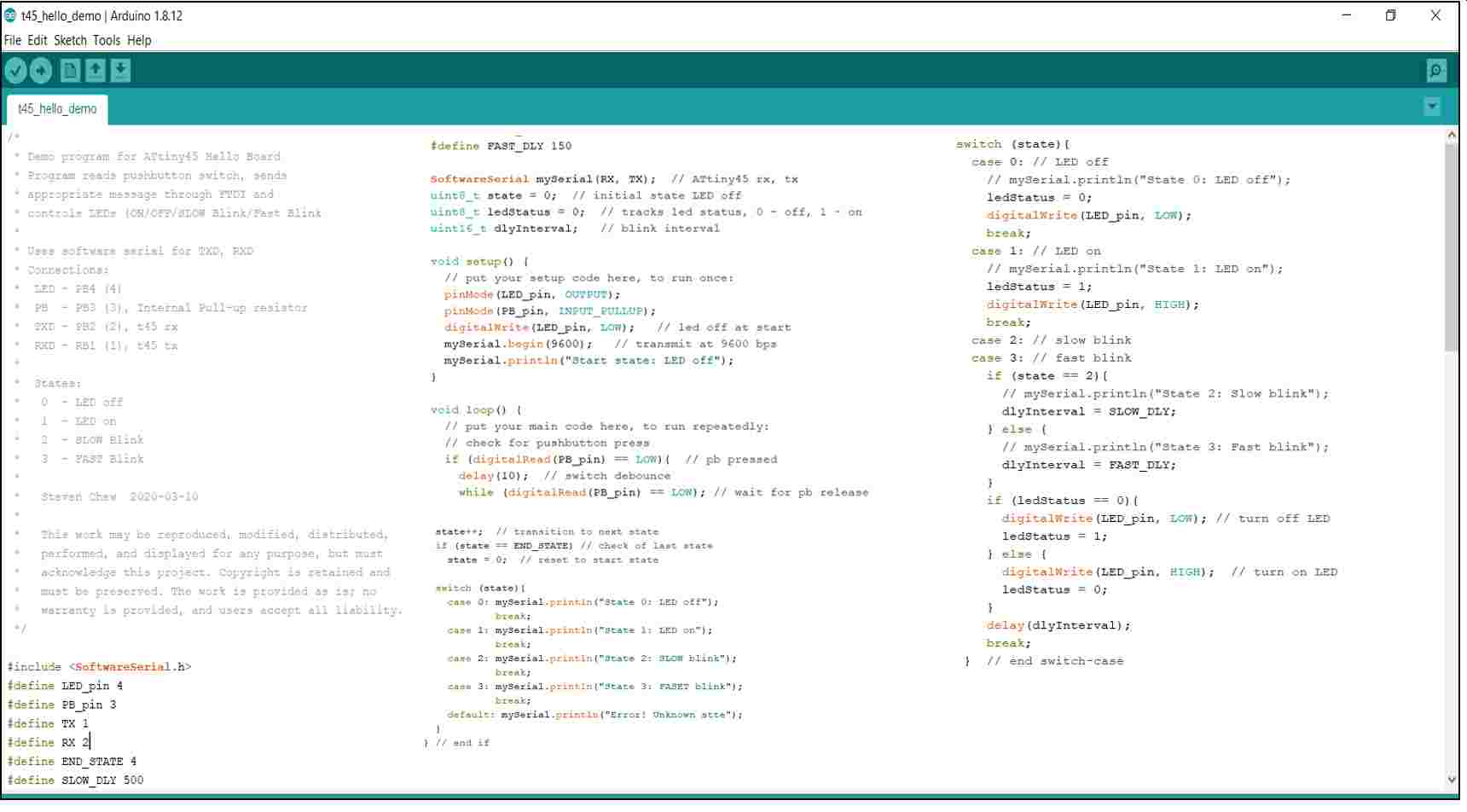
This program allows the button as well as the LED to be tested. When powered, the LED will light up indefinitely when the button is pressed once. On pressing the button a second time, the LED will blink slowly, at an interval of 500 milliseconds. When the button is pressed the third time, the LED will brink rapidly at an interval of 150 milliseconds.
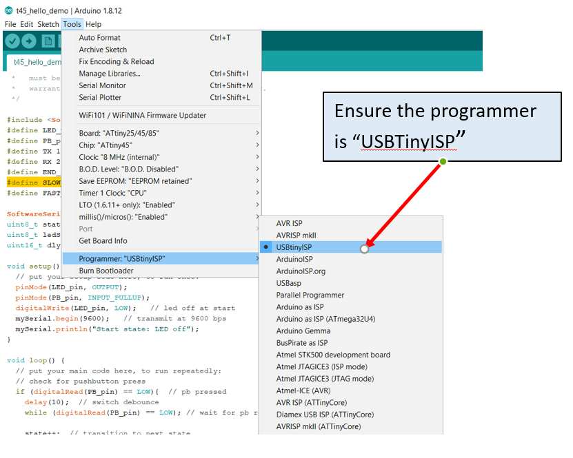
Before verify,compile and load the program to the board, it is important that the correct programmer is selected.
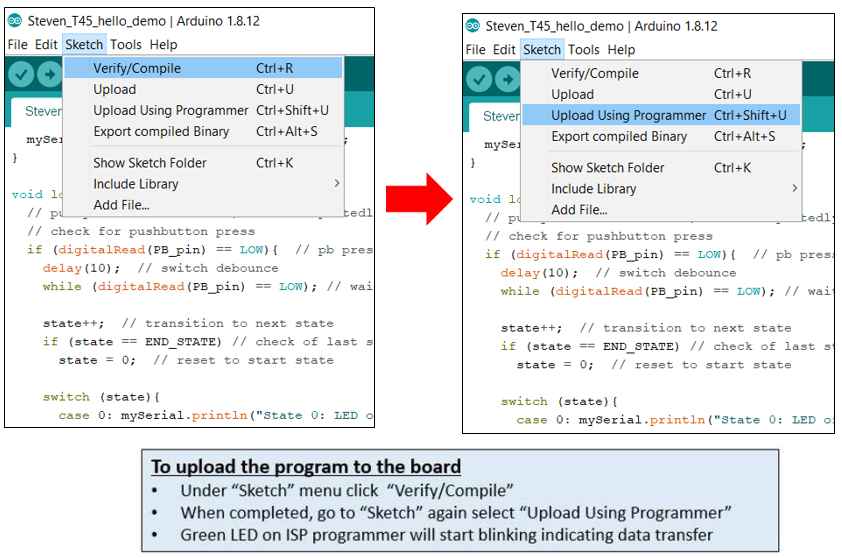
The program can now be uploaded into the board as per the steps shown in the image below
When uploading is completed, the board can be tested by pressing the button (once, twice and three times)
It Works!
Click Here to download the Arduino Sketch file that is written by my coach Steven.