Exercise 4 - Electronic Production 19/2/2020 to 25/2/2020
There are 2 tasks for this week:
- Group Assignment: Characterize the design rules for our PCB production process
- Individual Assignment: Make and test an in-circuit programmer by milling and stuffing the PCB
Task 1: Characterize the design rules for our PCB production Process
This is a group assignment done with Noel
Kristian and Yeo
Gau Siong.
Our collective work is documented on the SP
Fablab Website and hence only my learning
and reflections are documented here
What I have learned:
- ALWAYS secure the PCB board to be milled firmly on the sacrificial board using double-sided tape as well as masking tape.
- For drill bits with long shank, the feedrate MUST be set to very slow if
not it will snap during the milling process
- ALWAYS inspect the condition of the drill bit under the microscope before use.
- How to use MODS to convert the raw test file from raster
image format (*.png) to machine readable *.nc format
- Prepare and Operate the StepCraft 420 Milling machine
Task 2: Making and Testing an In-circuit programmer by Milling and Stuffing the PCB
Even though the assignment this week is simply to use one of
the designs from the Fab Academy class site to make a working
in-circuit progrmammer, being completely new to electronics, I
have to spend numerous hours just to understand some very basic
electronic concepts and to learn how to solder very tiny
components.
I chose to use ISP design from Brian's
site as the documentation was excellent and the tutorial is
easier to understand and follow. The fabrication process can be
broken down into several steps.
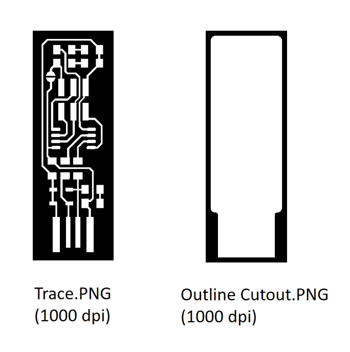
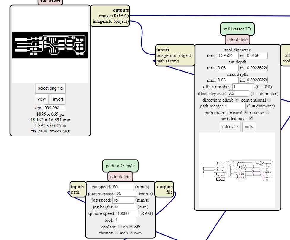
(A)
Creating the Milling Machine readable (NC) file &
cutting the PCB
Since the board layouts were already available from Brian's
site, I only need to use MODS to convert the raster file into
numerical control programming language format for the milling
machine.
 The method for
doing this is the same as that for the milling machine
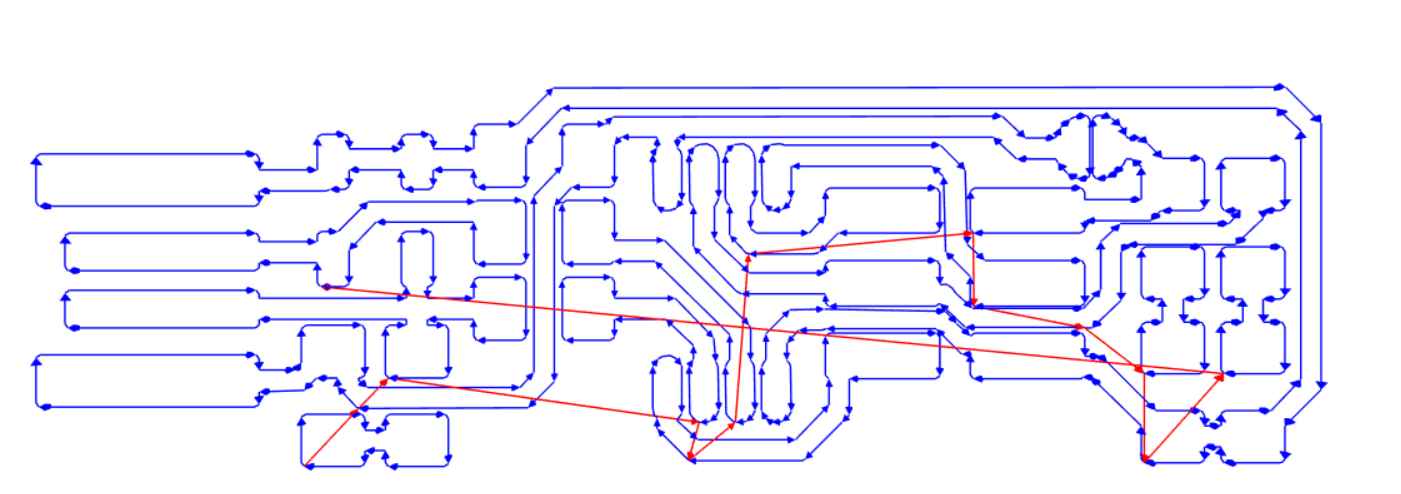
characterization and hence not included here. The preview of the
NC file is as follows:
The method for
doing this is the same as that for the milling machine
characterization and hence not included here. The preview of the
NC file is as follows:
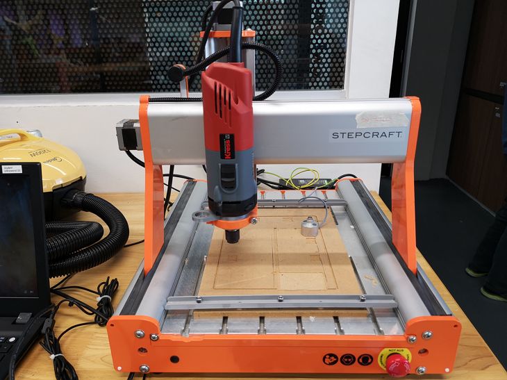
 After
obtaining this file, the trace is cut using the StepCraft 420
Milling machine. The settings are captured from the mods screen
below:
After
obtaining this file, the trace is cut using the StepCraft 420
Milling machine. The settings are captured from the mods screen
below:
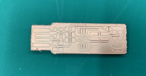
A 0.1mm 10 degree V-shaped drill bit was used.
(B)
Stuffing the PCB
Before soldering can be done, the "unwanted" or "dead" copper must be painfully removed using a penknife.
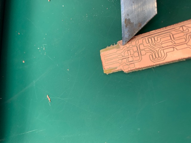
My local coach, Steven demonstrated a much easier way - By
increasing the number of passes (each offset by 0.5 diameter,
much of the "dead" copper can be cleared by the milling machine.
 As I am a newbie to soldering SMD, my
local coach Rodney, provided me a soldering training kit to hone
my skills before stuffing the PCB.
As I am a newbie to soldering SMD, my
local coach Rodney, provided me a soldering training kit to hone
my skills before stuffing the PCB.
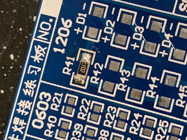
After practicing for a while, I started
stuffing the board using 0.6mm solder.
Components for the FabTinyISP are as follows:
1x ATtiny45
2x 1kΩ resistors
2x 499Ω resistors
2x 49Ω resistors
2x 3.3v zener diodes
1x red LED
1x green LED
1x 100nF capacitor
1x 2x3 pin header
Despite the practice, soldering such small parts for the first
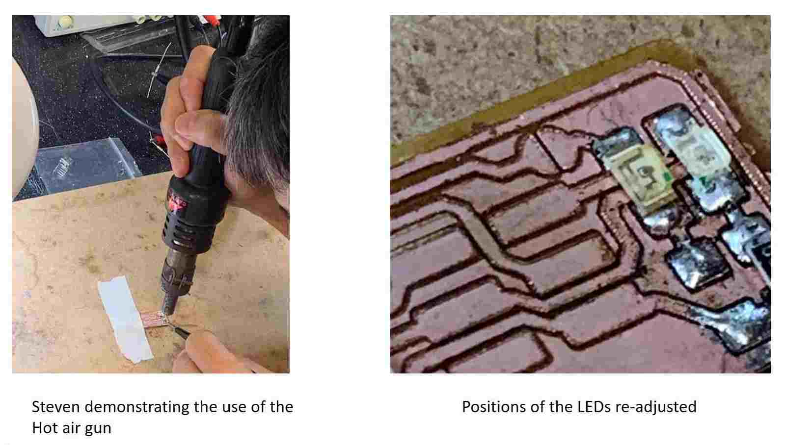
time was still very difficult and I made quite a few mistakes.
Thankfully, mistakes are not irrecoverable. My coach, Steven
demonstrated the use of the hot air gun to melt the solder on
the PCB board so that the positions of the components can be
adjusted or completely removed for re-soldering.
Serious Mistake!!
While soldering the 1K resistor, the solder went to the dead copper. In an attempt to remove the solder and the dead copper, I accidentally ripped the entire copper pad off the PCB board!
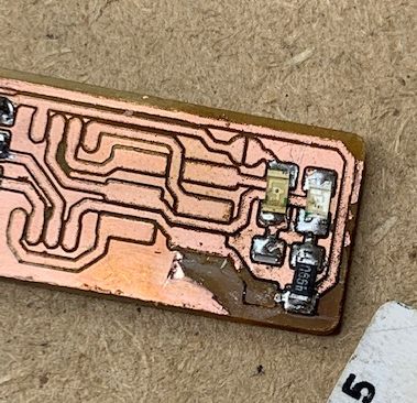
I have to redo the entire PCB from the beginning!
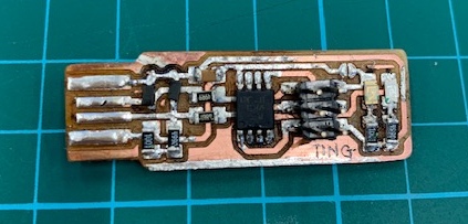
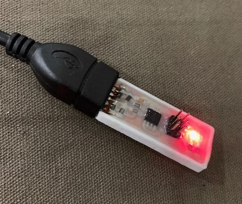
After 5 hours, the new PCB is finally stuffed. After my coach helped to check for short and rectified some bad soldering, I proceed with the third step: Software installation.
I designed a housing for the programmer in Fusion 360 and 3D printed it. I then encapsulated it with clear epoxy
(C)
Software Installation
- GNU Toolchain - (from Microchip.com
instead)
- GNU
Make
- Avrdude - For Avrdude, the Avrdude.exe downloaded according
to Brian's guide does not seems to work for my laptop, I have
to install WinAVR from Sourceforge.net
first and locate the avrdude.exe file from the Bin folder in
WinAVR
- Firmware
Source Code
After installing the softwares, I have to edit the windows search Path so that all the required software can be located when their names were type on the command line. To do this, I followed the guide from Brian's site again. (Control Panel -->System -->Advanced System Settings-->Environment Variables). The following 3 items were added to the search path:
- C:\Program Files\avr8-gnu-toolchain\bin
- C:\Program Files (x86)\GnuWin32\bin
- C:\Program Files\avrdude
Following that, I go to gitbash and carried out the following steps in the order as according to Brian's guide
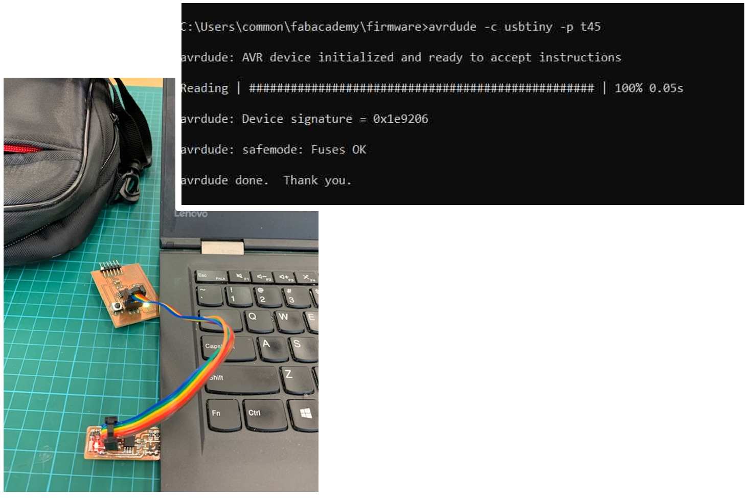
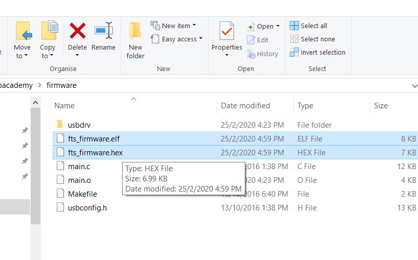
- Connect the programmer to a USB port and type: avrdude -c usbtiny -p t45.
- Run "make" under GIT. This created the fts_firmware.hex file and the fts_firmware.elf file.
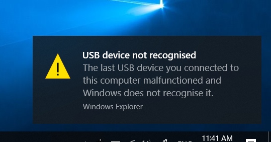
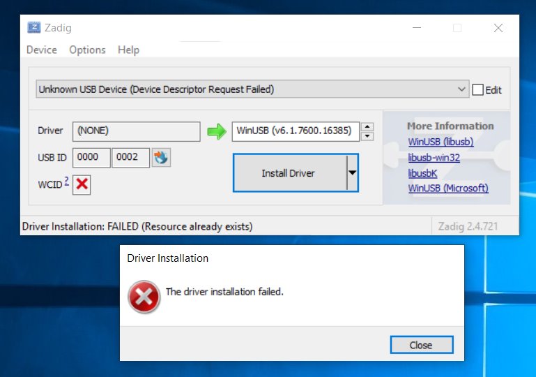
An error "Could not find USBtiny device (0x1781/0xc9f)" was found. This error was described by Brian in his guide. Following his instruction, I downloaded Zadig to check and update the USB driver installation.
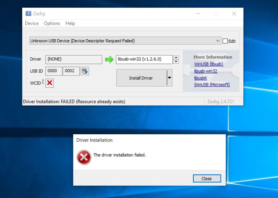
After this step, I inserted the programmer into the USB port of the laptop
I run Zadig again and tried to install libusb-win32 driver and
winusb driver, but both installations failed.
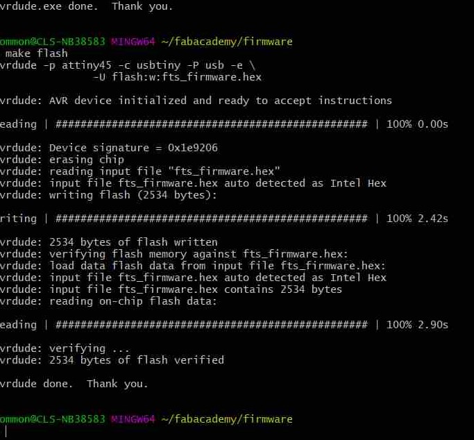
After troubleshooting, it was found that the header was not properly soldered and contact was intermittent. After touching up the solder, the PCB can now be recognized and I can continue with the software installation. In gitbash, I entered "make flash" to upload the firmware into the PCB (target).
This command upload the fts_firmware.hex file into the chip. The "make flash" command basically execute the avrdude program as per the command line "avrdude -c usbtiny -p t45 flash:fts_firmware.hex:i"
After running "Make Flash" the next step is to configure the
chip using the "Make fuses" command. This command like "make
flash" run the following avrdude command: "avrdude -c usbtiny -p
t45 lfuse:w:0xE1:m -u hfuse:w:0xDD:m -U efuse:w:0xFF:m"
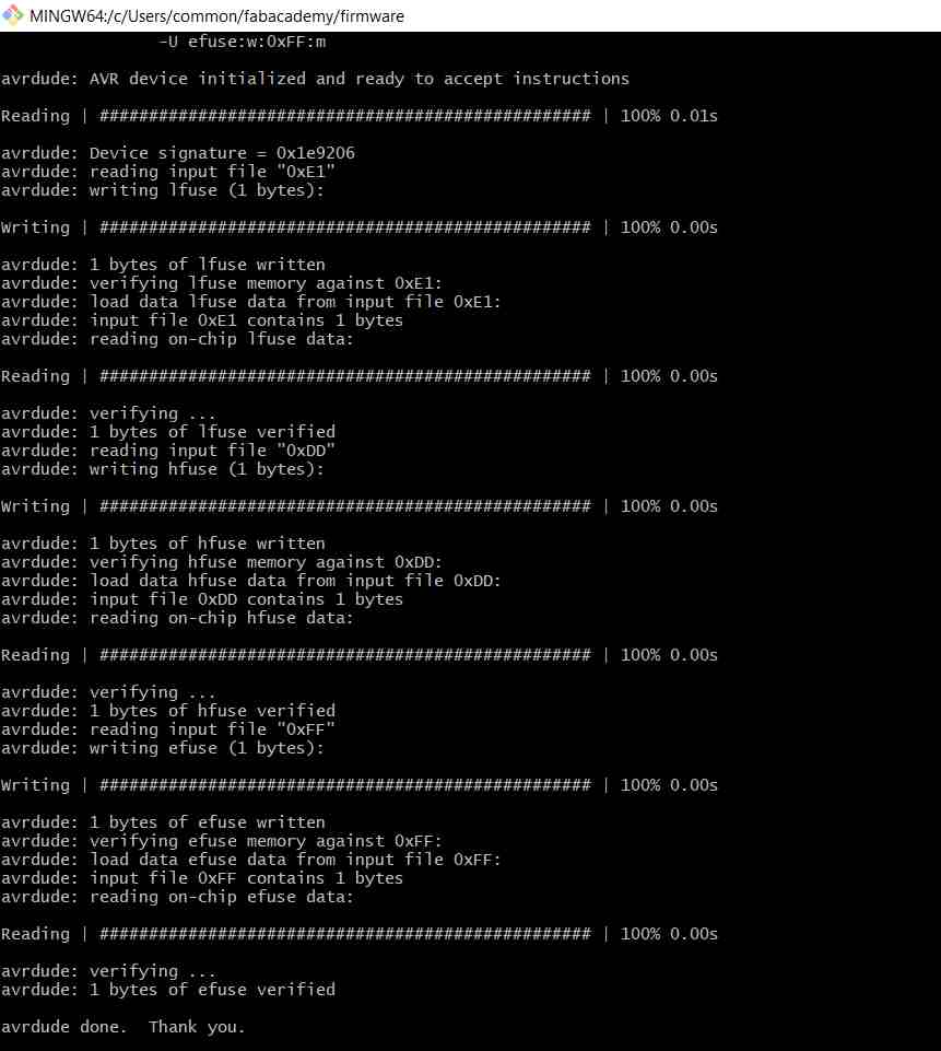
After this step, I inserted the PCB into the laptop usb port and to my delight, the device is detected and recognised!

The final step is to disable the reset fuse (or blow the fuse,
as described by Brian). To do this, I have to run the command
"make rstdisbl"
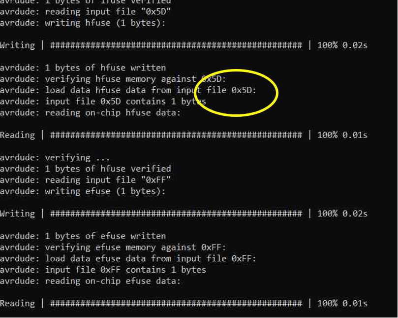
Resetting the fuse changes the ATtiny45's reset pin into a I/O pin. This action will disable the ability to reprogram the ATtiny45 chip in the future. To do this, the existing programmer is again used and my PCB is connected as the target.
The software installation is finally completed and my PCB can now be used as a programmer! I tested it on a target board and it worked!