Electronics Design
Group assignment
- Use the test equipment in your lab to observe the operation of a microcontroller circuit board (in minimum, check operating voltage on the board with multimeter or voltmeter and use oscilloscope to check noise of operating voltage and interpret a data signal)
- document your work (in a group or individually)
group project here
Individual assignment
- Redraw one of the echo hello-world boards or something equivalent, add (at least) a button and LED (with current-limiting resistor) or equivalent input and output, check the design rules, make it, test it.
KiCad
learned how to make circuits using KiCad.
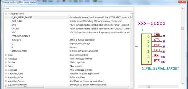
Downloading the library was the first step in creating a circuit.
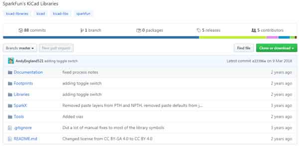
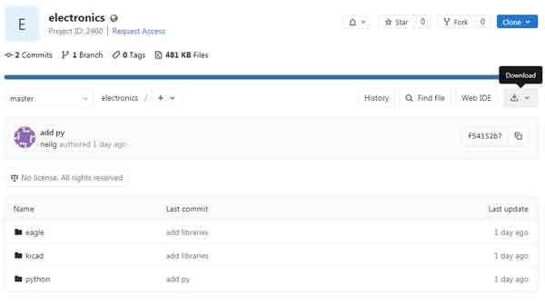
You could download the library from Sparkfun KiCad library, Digiki KiCad library, and pub electronics.
Sparkfun KiCad library
Digiki KiCad library
pub electronics

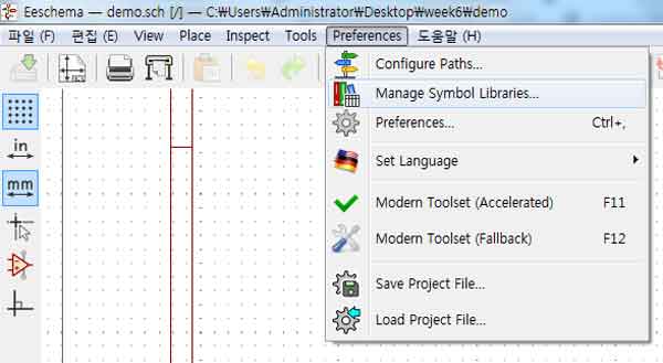
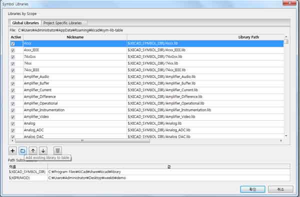
 You can add Libraries through the Manage Symbol Libraries in Preferences of the KiCad Program.
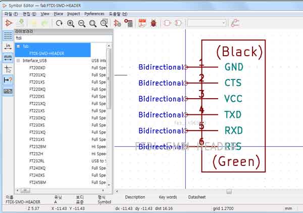
 The added library was checked and circuit creation started.
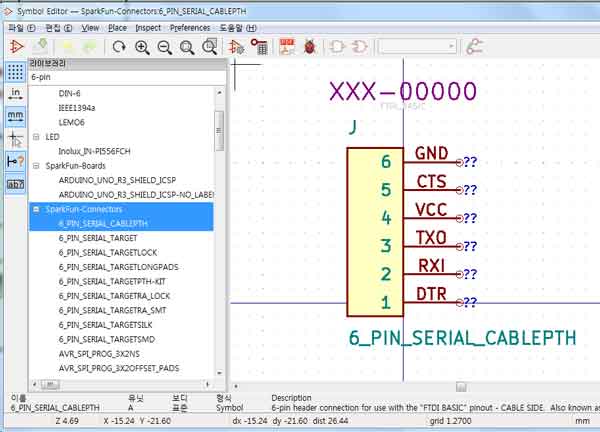
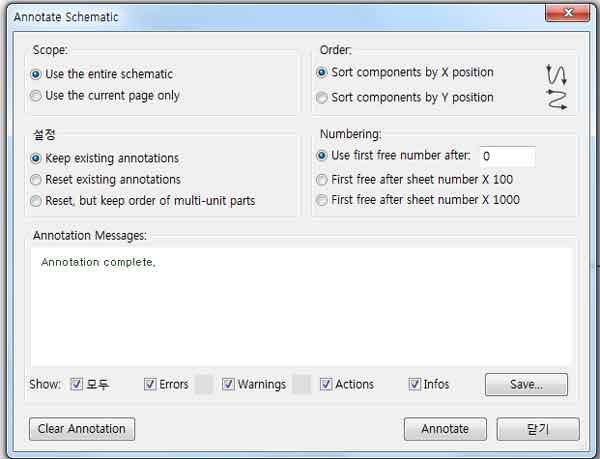
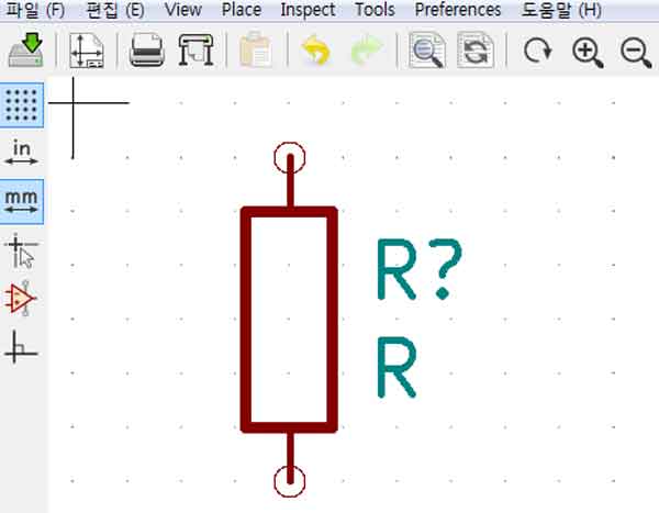 The circuit is also finished with the design and annotated using Annotate schematic symbols.
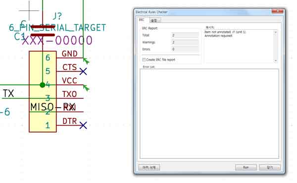
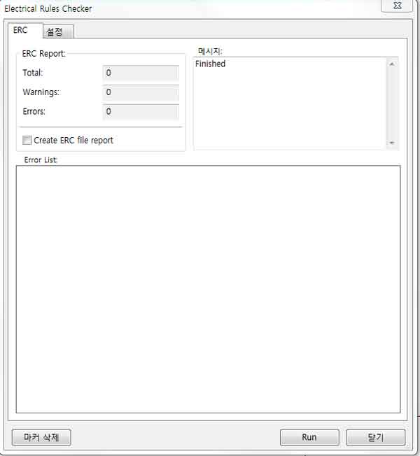
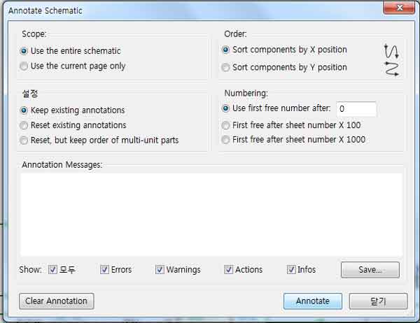 After annotating it, I checked the electronic rules.
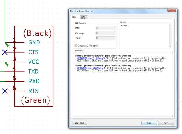 The problem of pin 1 and pin 3 being bidirectional connected was found, but there was no problem with the circuit design.
Unable to find the problem, I asked Craig for help and he found the problem, saying that there would be a problem with the parts.
The problem of pin 1 and pin 3 being bidirectional connected was found, but there was no problem with the circuit design.
Unable to find the problem, I asked Craig for help and he found the problem, saying that there would be a problem with the parts.
 I was able to change the parts and solve the problem.
 I had to reconnect the parts because of the changed parts.
After finishing the connection, I checked the electronic rules again.
I had to reconnect the parts because of the changed parts.
After finishing the connection, I checked the electronic rules again.
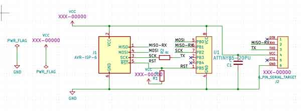
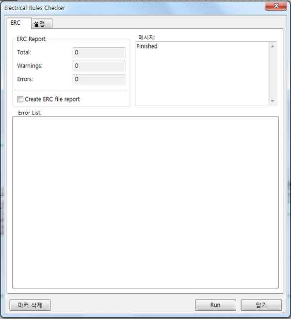 Clear!
Now that i have learned how to use the kicad, design and test a new board!
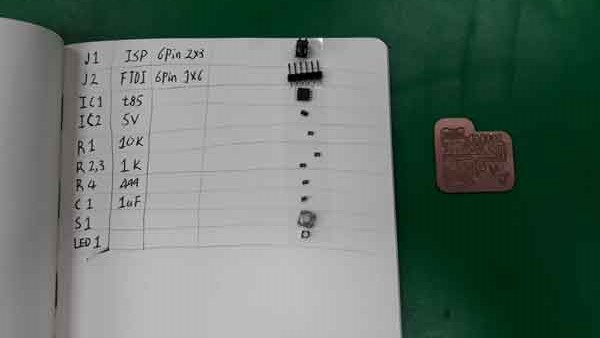
I made a new board by referring to the input, output devices design.
Clear!
Now that i have learned how to use the kicad, design and test a new board!
I made a new board by referring to the input, output devices design.
Input Devices
Output Devices
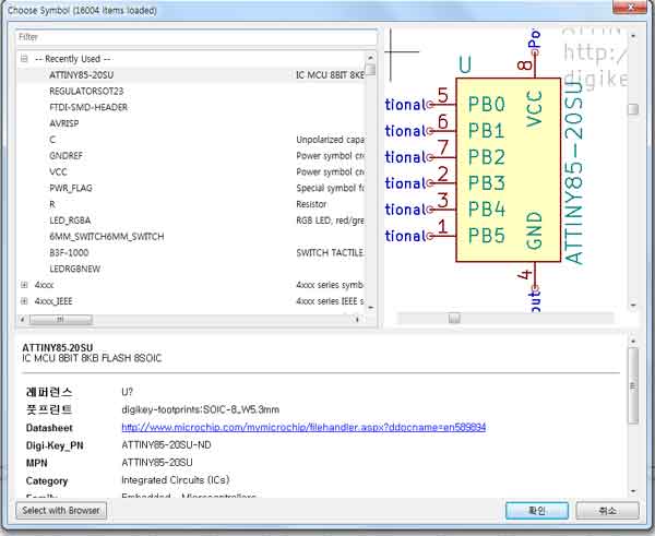
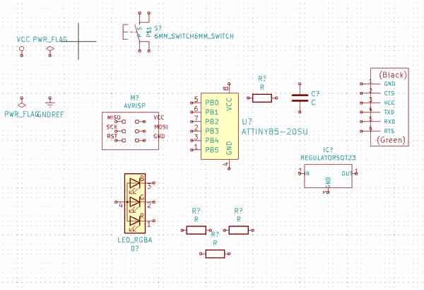
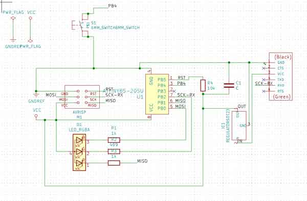
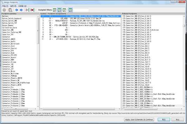
 I found the parts for the board, connected them to each other, and checked the electronic rules.
The part was selected using assign PCB footprints to schematic symbols.
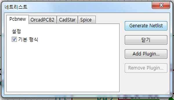
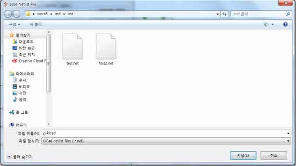
I saved it as a net file using the generate netlist
I found the parts for the board, connected them to each other, and checked the electronic rules.
The part was selected using assign PCB footprints to schematic symbols.
I saved it as a net file using the generate netlist
.jpg)
.jpg)
 run pcbnew to layout printer circutr board and Bring saved net file
.jpg)
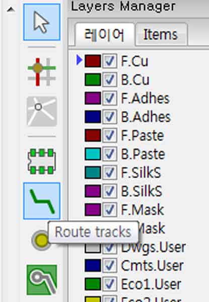
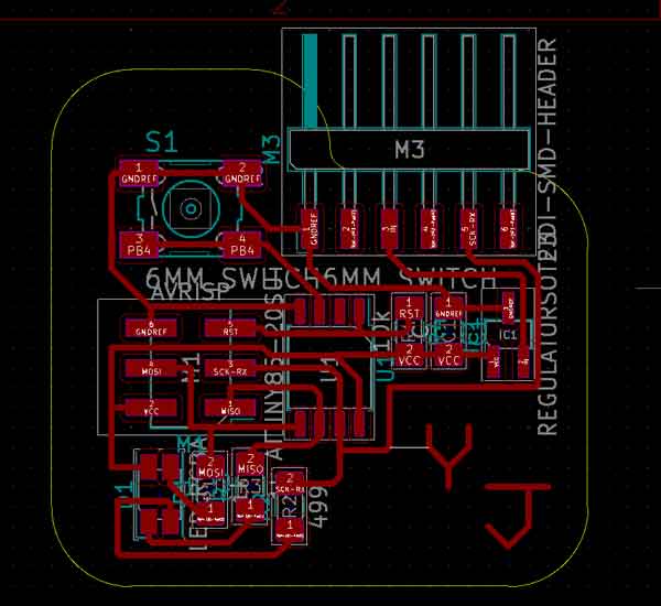
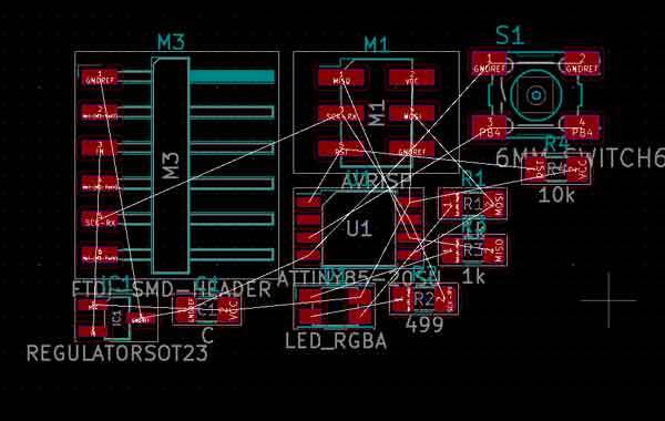 I connected the part using route tracks.
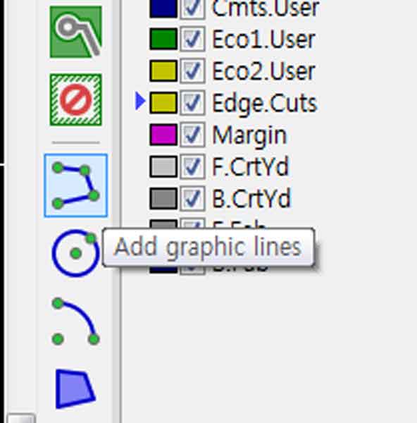
After connecting parts, add graphic lines were used to create the edge of the board.
I connected the part using route tracks.
After connecting parts, add graphic lines were used to create the edge of the board.
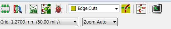
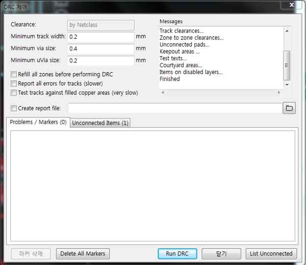
 Run DRC using the performance design rules check.
.jpg)
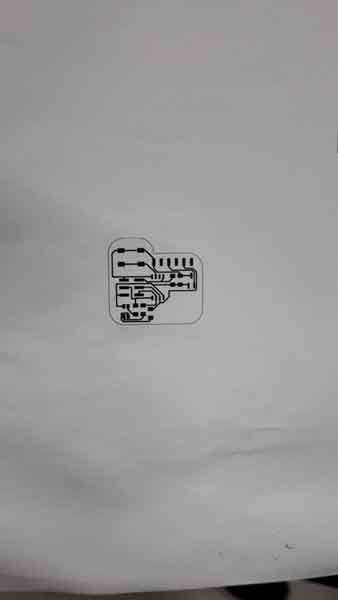
 Using a print board, print the board and make sure it fits the parts to be used and the board design.
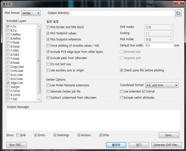
 Use the plot to plot the board design.
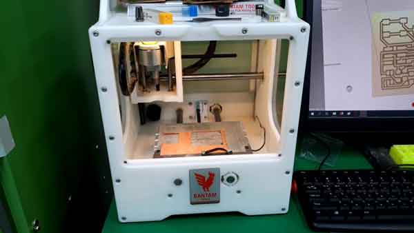
Bantam was used to make a board
Use the plot to plot the board design.
Bantam was used to make a board
.jpg)
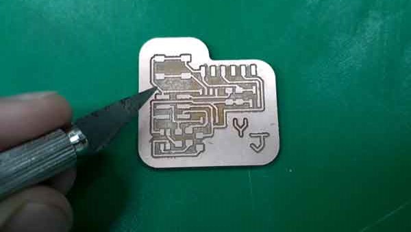
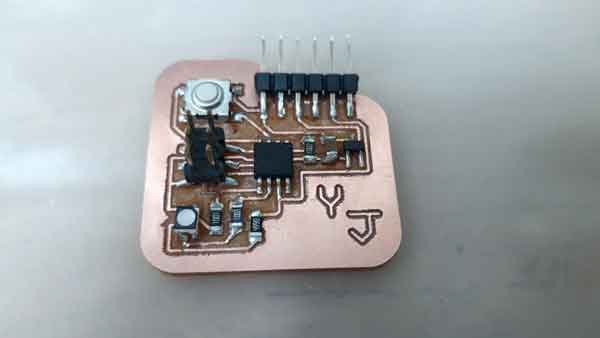
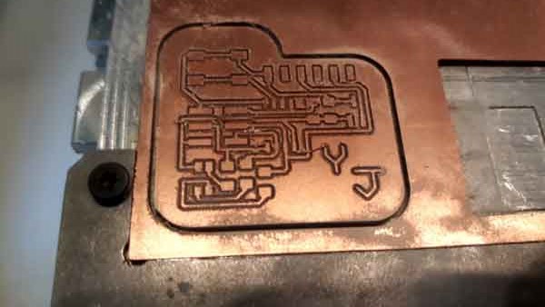 I checked the board and used a carving knife.
 I soldered the parts to the board.
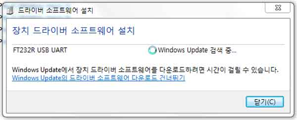
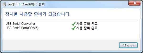
 I connected the new board to the my laptop and the driver was installed automatically.
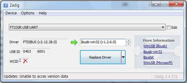
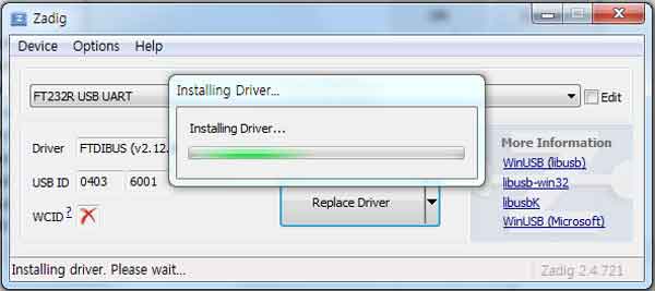
I reinstalled driver using zadig
I connected the new board to the my laptop and the driver was installed automatically.
I reinstalled driver using zadig
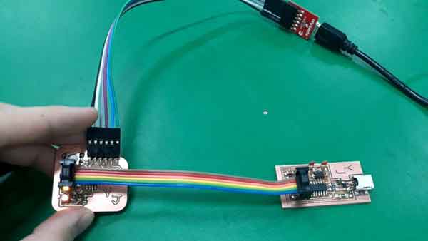
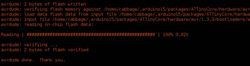
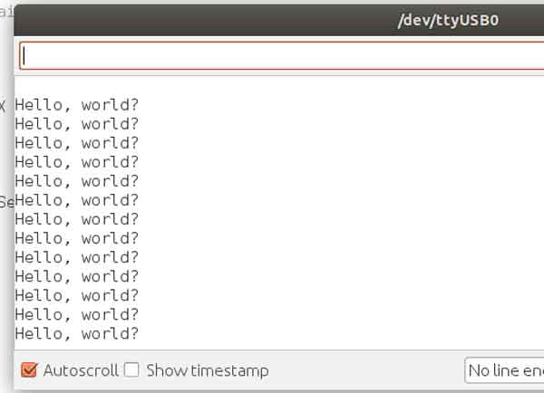
 I didn't know about programming, but with the help of Craig, I was able to check if programming was possible on the new board.
 Thank you, Craig
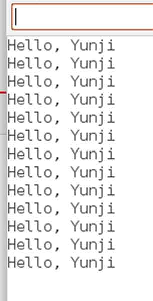
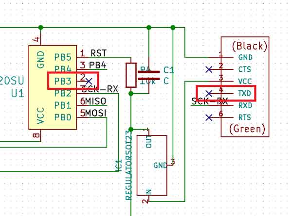
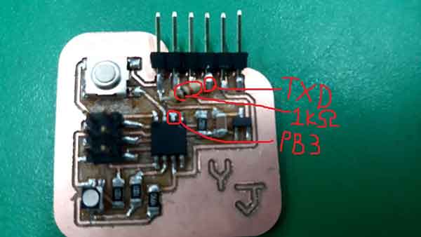
I could program without a problem, but there was a design problem on my board
I should have connected the PB3 and TXD, but my board design was not connected to the PB3 and TXD As a solution, Craig taught me how to jump resistance onto a board and connect it, and I solder it
Thank you, Craig
I could program without a problem, but there was a design problem on my board
I should have connected the PB3 and TXD, but my board design was not connected to the PB3 and TXD As a solution, Craig taught me how to jump resistance onto a board and connect it, and I solder it
my work
yj-kicad pcb File here
yj-kicad File here
yj-kicad Edge_Cuts File here
yj-kicad F_Cu File here