
Week 7 Electronic Design
This week is proberbly the most diffcult week for me. Electronics are mystery. Design and making my own electronic board is quite challenging for a person like me who studied literature in university.
Weekly Assignment
- Group assignment: use the test equipment in your lab to observe the operation of a microcontroller circuit board
- Individual assignment: redraw an echo hello-world board, add (at least) a button and LED (with current-limiting resistor) check the design rules, make it, and test it
Software or tools I learned:
Download Eagle
EAGLE (Easily Applicable Graphical Layout Editor) is a flexible and expandable EDA schematic capture, PCB layout, autorouter and CAM program. EAGLE is popular among hobbyists because of its freeware license and rich availability of component libraries on the web.
What's a PCB?
Printed circuit board is the most common name but may also be called "printed wiring boards" or "printed wiring cards". Before the advent of the PCB circuits were constructed through a laborious process of point-to-point wiring. This led to frequent failures at wire junctions and short circuits when wire insulation began to age and crack.
A significant advance was the development of wire wrapping, where a small gauge wire is literally wrapped around a post at each connection point, creating a gas-tight connection which is highly durable and easily changeable.
As electronics moved from vacuum tubes and relays to silicon and integrated circuits, the size and cost of electronic components began to decrease. Electronics became more prevalent in consumer goods, and the pressure to reduce the size and manufacturing costs of electronic products drove manufacturers to look for better solutions. Thus was born the PCB.
PCB is an acronym for printed circuit board. It is a board that has lines and pads that connect various points together. In the picture above, there are traces that electrically connect the various connectors and components to each other. A PCB allows signals and power to be routed between physical devices. Solder is the metal that makes the electrical connections between the surface of the PCB and the electronic components. Being metal, solder also serves as a strong mechanical adhesive.
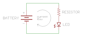
What is a circuit?
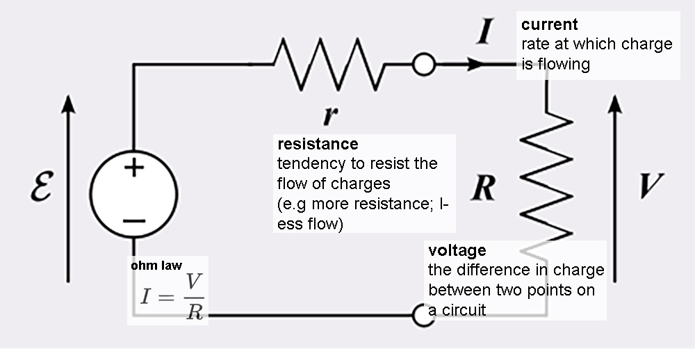
Electricity is briefly defined as the flow of electric charge.Electricity can only flow through materials that can conduct electricity, such as copper wire. Electricity wants to flow from a higher voltage to a lower voltage.If you create a conductive path between a higher voltage and a lower voltage, electricity will flow along that path. A circuit is a closed loop that allows charge to move from one place to another. Components in the circuit allow us to control this charge and use it to do work.
Composition
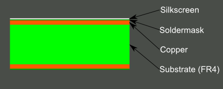
A PCB is sort of like a layer cake or lasagna- there are alternating layers of different materials which are laminated together with heat and adhesive such that the result is a single object.
Electrical Charge
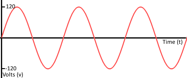
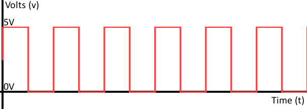
Analog vs. Digital
Signals are passed between devices in order to send and receive information, which might be video, audio, or some sort of encoded data. Usually the signals are transmitted through wires, but they could also pass through the air via radio frequency (RF) waves. Audio signals, for example might be transferred between your computer's audio card and speakers, while data signals might be passed through the air between a tablet and a WiFi router.
We live in an analog world. There are an infinite amount of colors to paint an object (even if the difference is indiscernible to our eye), there are an infinite number of tones we can hear, and there are an infinite number of smells we can smell. The common theme among all of these analog signals is their infinite possibilities.
Digital signals and objects deal in the realm of the discrete or finite, meaning there is a limited set of values they can be. That could mean just two total possible values, 255, 4,294,967,296, or anything as long as it's not ∞ (infinity).
Further more , you can read tutoriel
List of materials
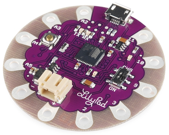
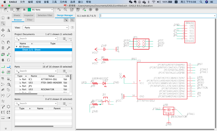
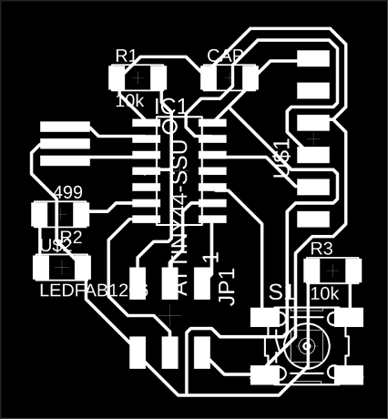
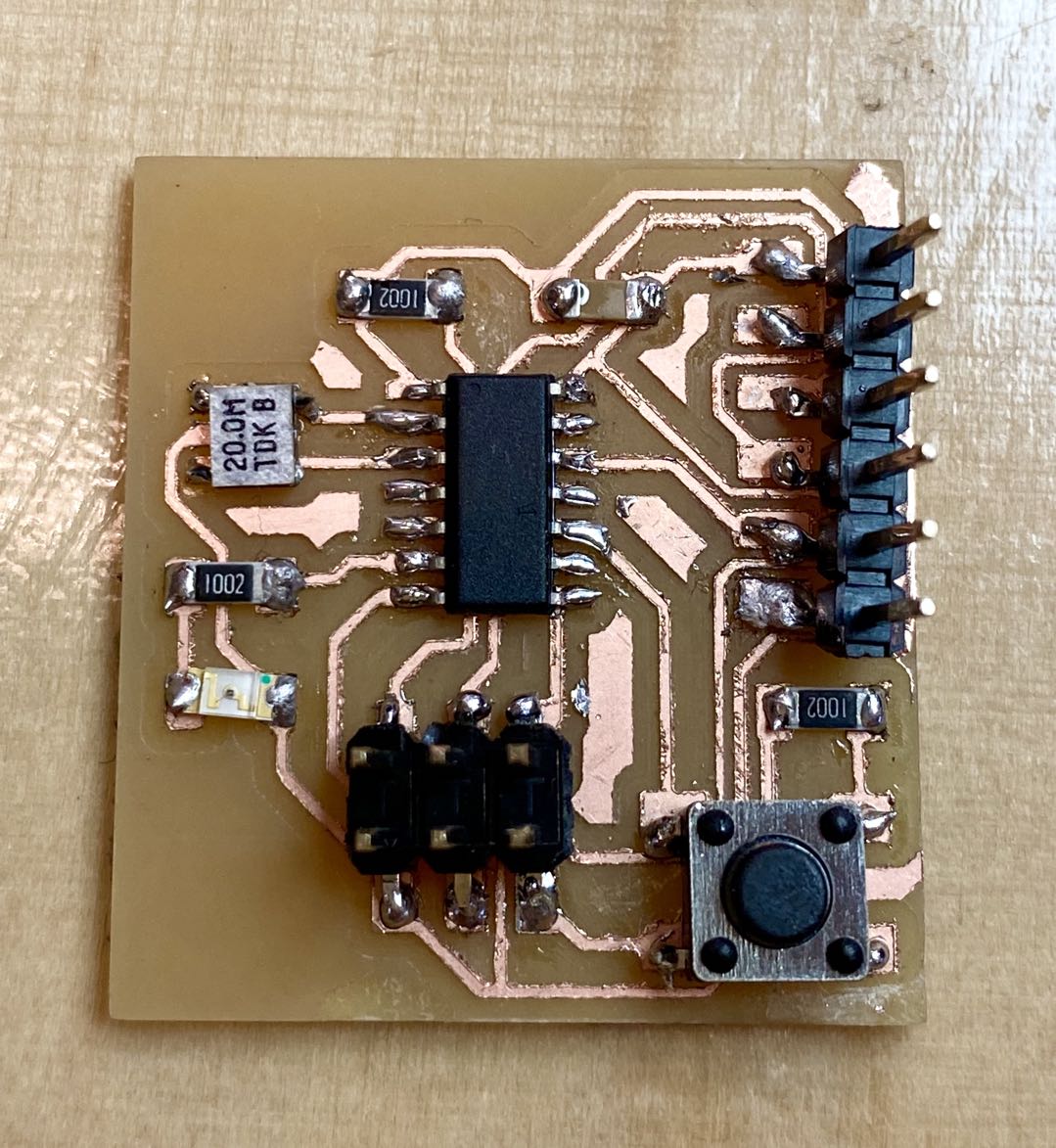
- ATtiny44: microcontroller, it's like the brain of the circuit. It is a programmable component that we will program afterwards from the computer. On the diagram it appears with the tag of IC1t44.
- Resistor of 10k/10 Ohm: For reduce the flow of the current, keep steady the flow that goes into the microcontroller near VCC and for the RESET signal.
- FTDI: It connects a special cable (FTDI cable) that serves to connect the microcontroller to a USB port and translate the serial language from the MCU to USB language
- SPI header pin(Serial Peripheral Interface): it's connect MCU to your FABISP to take the data needed, so you will see that MOSI, MISO and SCK (input and output pins) connect to your MCU. You will notice that it has to be connected also to GND and VCC. SPI basically serves for communication between MCU and other peripheral devices.
- Crystal Or resonator(XTAL): an external clock and it emits a signal at certain frequency (hertz). MCU have a built in clock but external resonators are used to have a more accurate clock. This frequency will tell the MCU how fast/slow to execute a task. It is connected to theh free pins on the MCU PB0 and PB1, and needs to be connected to GND.
- LED+10 Ohm resistor+ button : We add one LED and a button to make it a little bit more complex.
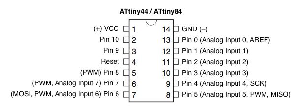
VCC (voltage at the common collector) it is where circuits get their voltage. In our case the voltage comes from another device and commonly the main power input is 5V; GND (ground) as the name says is the base 0V level; SCK, serial clock to synchronize the data that is being "spoken" among the ISP and your new microcontroller; MOSI is the output; MISO is the input. TX : transmit RX: receive
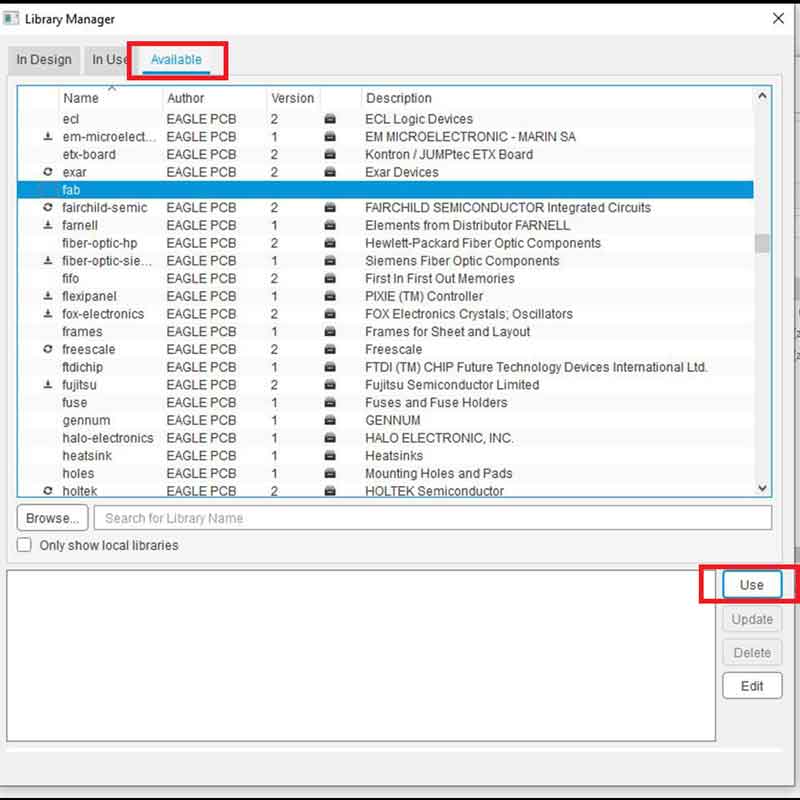
Add library in Eagle
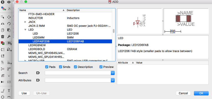
To use those conponents symbols, we add a fab library in our eagle.go to Library>Open Library Manager, remove the ones that are inside "IN USE", it won't delete them just remove from the available components in the library. Then go to AVAILABLE and browse the FAB library and select USE, this will add it to your EAGLE library:
Eagle commands
Eagle is like a drawing software for electronics. You draw on eagle and use CNC machine engrave board following the schematic you drew, and then soldering conponents on board so this board can work. First you need to know schematic symbols.
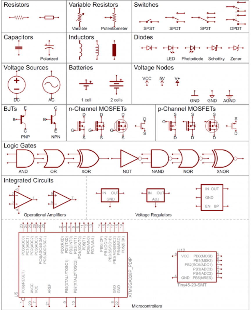
Just like learn other drawing software you need to know those commands:
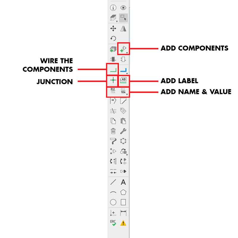
- add = opens up the libraries so that you can add components in Schematic view.
- move = moves an item
- net = makes a logical connection
- junction = adds a junction
- value = addes value to components (i.e. ohm rating)
- name = names a component
- label = displays the name of a component in schematic view
- copy = copies an existing component on the schematic.
- route = used in Layout view, this tells you if you need to add a connection (follow yellow lines)
- ERC = electronic rules check; this ensures your board will actually work (use in schematic view)
- DRC = design rules check (in board view) - keep all the default settings (16 mil is fine); it should display a "no error" message in the bottom left hand corner of the screen
- group = groups components in Layout view together; if you right-click, then you can choose Move: Group to move the grouping
- rats = in board view, tells you if you have airwires.
- rip = deletes connections in layout
- show = after typing this, select a component to see information about it displayed in the bottom left corner of the screen. Also, if you type show + [name of component] you can see that component highlighted. You can use this to see all the ground traces, for example.
- text = allows you to add text to your board. You can also edit the exported .png file in The Gimp to give text and black and white line images. I recommend adding text in The Gimp.)
- info = then click on text to get properties of the text
Process of drawing schematic
- Add components to the schematic view and create connections between them. You need to find a conponents library online if you don't already have it. We use fab.lbr library
- Verify the design using the ERC (Electrical Rules Check)
- Connecting the components and fixing any errors, then will go into the board view and place the components and route the traces.
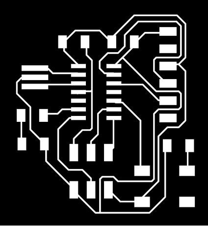
- Route traces on a board, switch to the board view,go to the top menu > File > switch to board. The components you just added will be jumbled up in a corner with yellow unrouted traces attached
- Design rules check and Exported PNG, Creating Traces and Mill-out Files.
- Add a White Border around the image for CNC to cut.

Set machine paths
Used the Fabmodules online to calculate the machine paths and set input and output to milling the board.
Milling the board
Turn on Roland Modela and the computer and open VPanel for SRM-20,A nice tip is to warm the spindle for 10 min at mid Rpm before using it.,
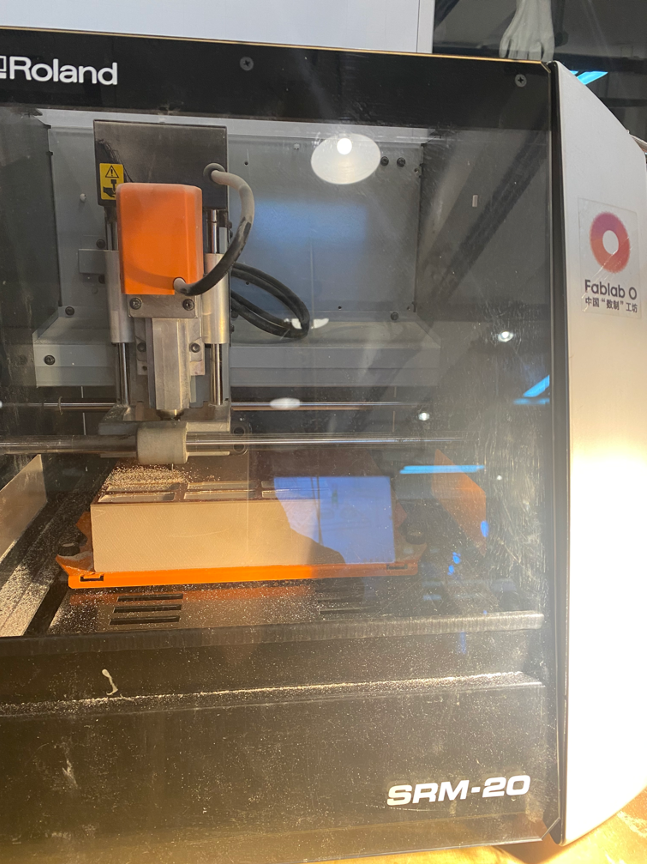
Change mill: 1/32 inch bit is for cutting out board,1/64 inch bit for milling trace;Set the X/Y/Z zeros;Send the traces and send the outcut/holes.
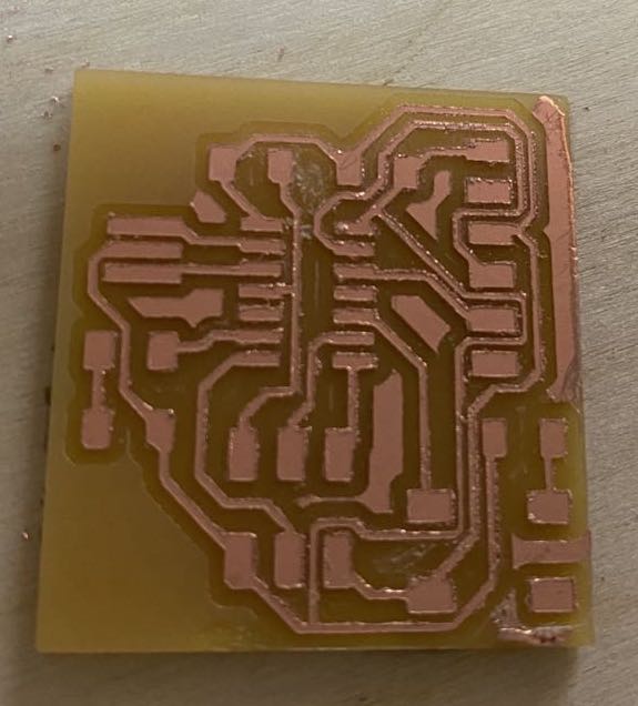
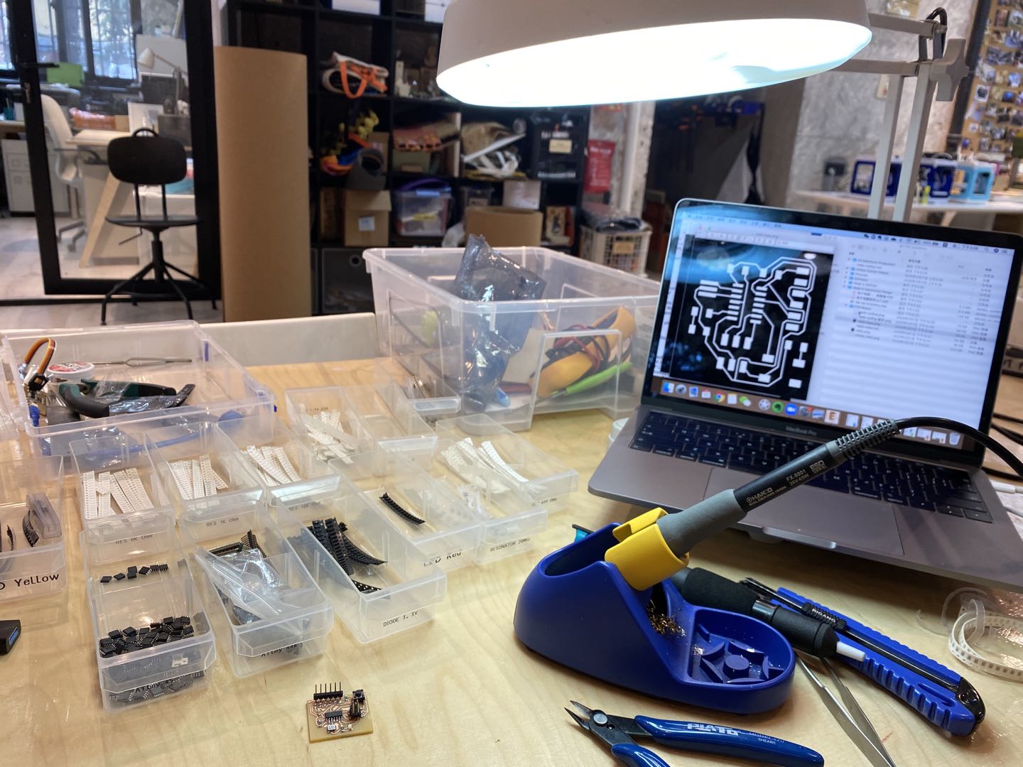
Soldering the board
Use tweezers and brush to clean and remove glitch.
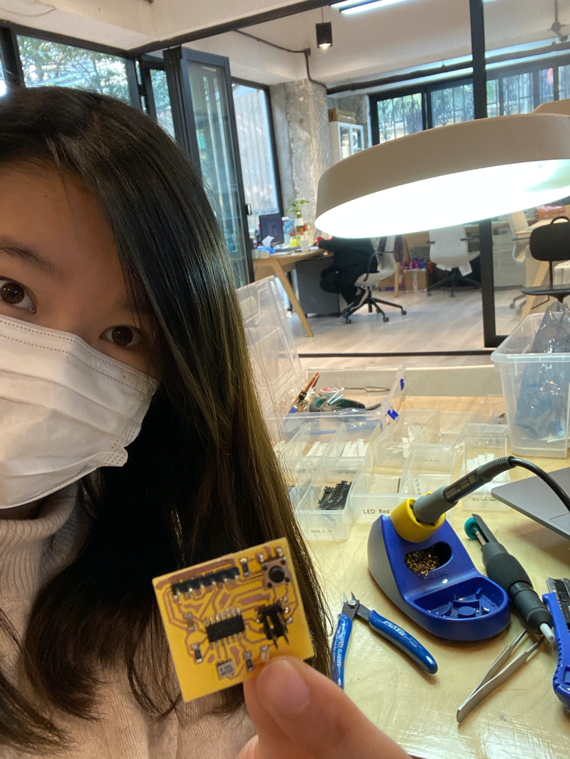
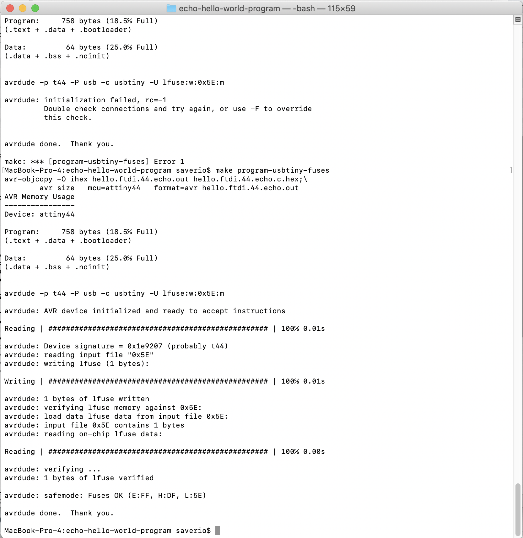
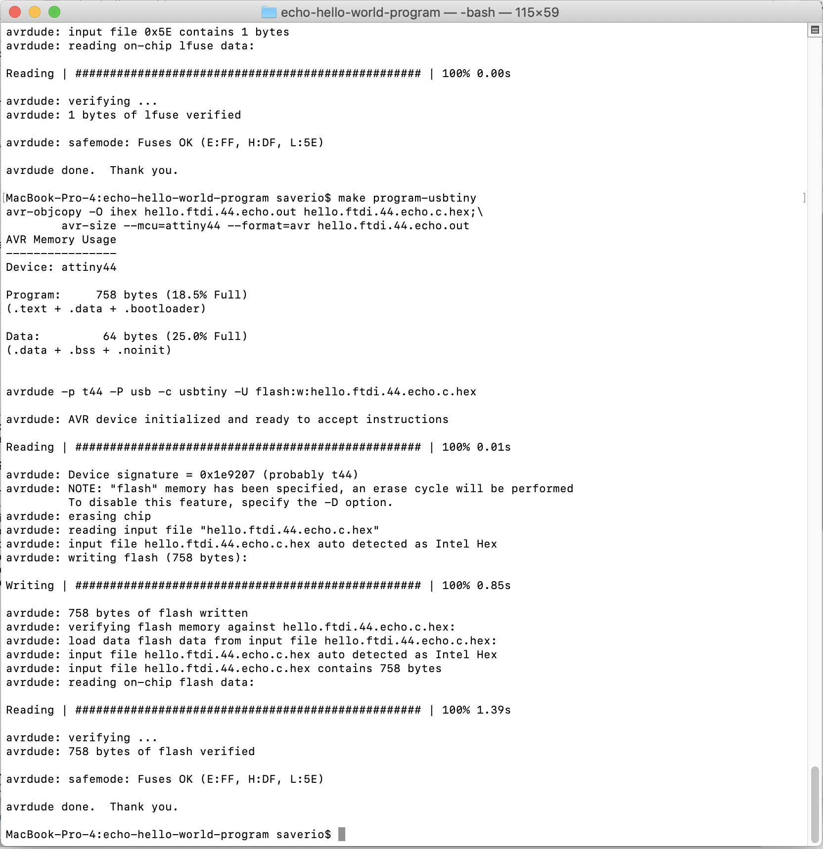
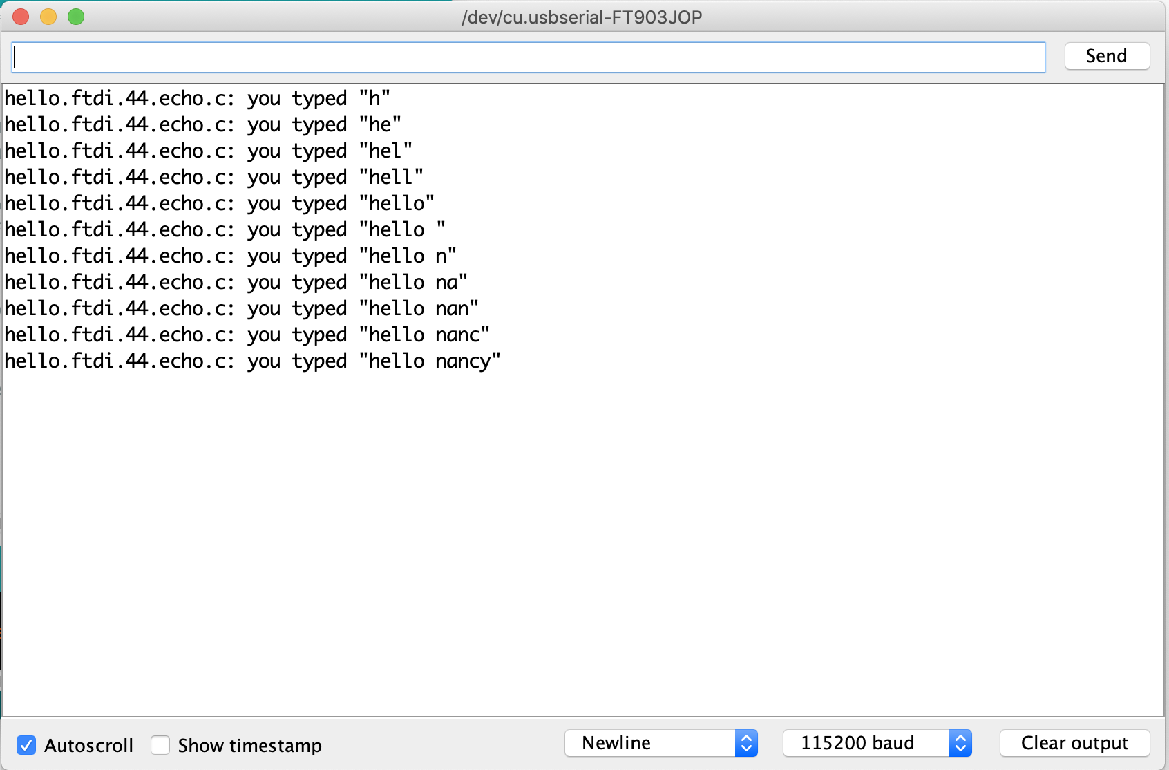
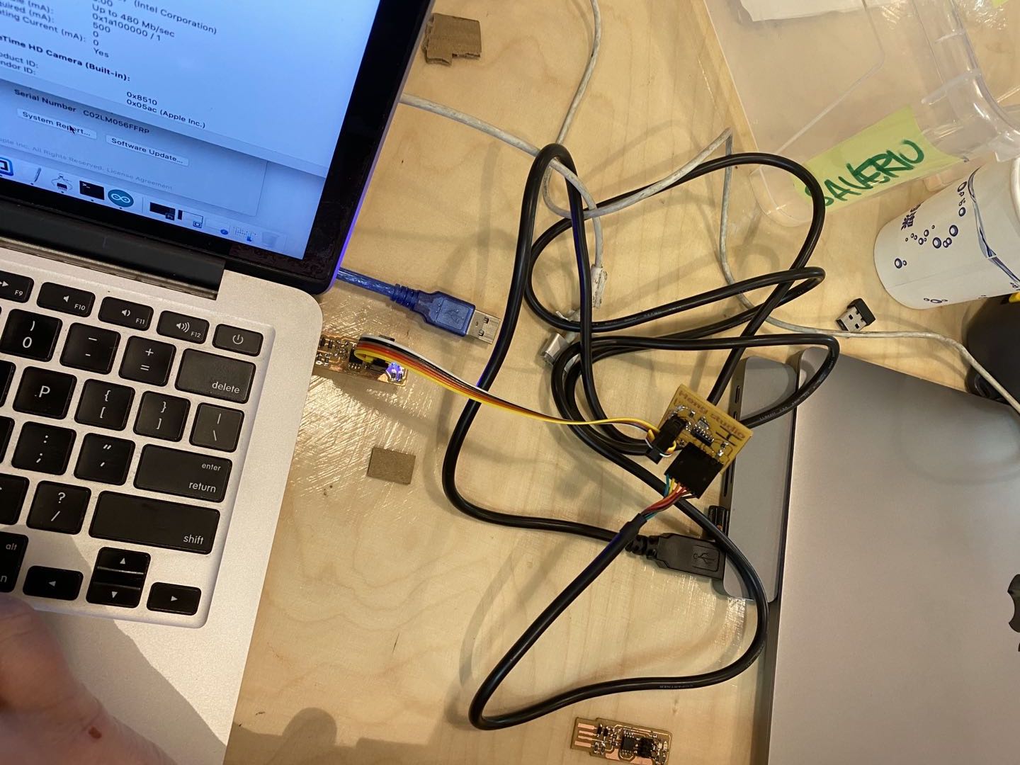
Test the echo hello board
Conect hello board with isp.
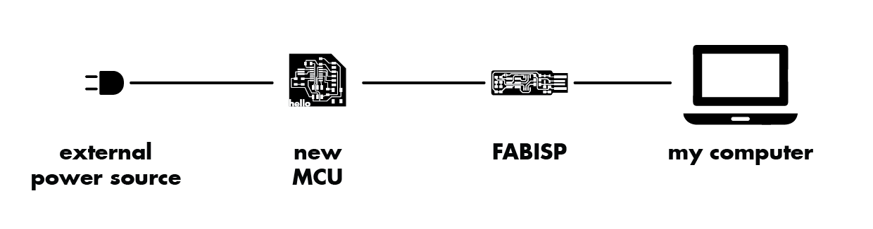
Tpye those code in terminal:
make -f hello.ftdi.44.echo.c.make make -f hello.ftdi.44.echo.c.make program-usbtiny-fuses make -f hello.ftdi.44.echo.c.make program-usbtiny
It's working well: